

M54HC4538
M74HC4538
DUAL RETRIGGERABLE MONOSTABLE MULTIVIBRATOR
.HIGH SPEED
tPD= 25 ns(TYP.) AT VCC=5V
.LOWPOWERDISSIPATION
STANDBYSTATEICC=4µA(MAX.)ATTA=25°C
ACTIVESTATE ICC=200µA (TYP.)ATVCC=5V
.HIGH NOISEIMMUNITY
V
NIH=VNIL
.OUTPUT DRIVE CAPABILITY
10 LSTTL LOADS
=28%VCC(MIN.)
B1R
(PlasticPackage)
(CeramicPackage)
.BALANCEDPROPAGATION DELAYS
t
PLH=tPHL
.WIDE OUTPUT PULSE WIDTHRANGE
t
=120ns ~ 60 sOVER ATVCC=4.5V
WOUT
.OUTPUT PULSE WIDTH INDEPENDENT
FROM TRIGGERINPUT PULSE WIDTH
.PIN ANDFUNCTION COMPATIBLE
WITH 4538B
M1R
(MicroPackage)
ORDER CODES :
M54HC 4538F1R M74H C4538M1R
M74HC 4538B1R M74HC4 538C1R
(Chip Carrier)
F1R
C1R
DESCRIPTION
The M54/74HC4538 is a high speed CMOS DUAL
MONOSTABLEMULTIVIBRATOR fabricatedinsilicon gate C2MOStechnology. It has the same high
speed performance of LSTTL combined with true
CMOS low power consumption. Eachmultivibrator
featuresboth a negative, A, and a positive, B, edge
triggered input, either ofwhichcanbeused asaninhibit input. Also included is a clear input that when
taken low resets the one shot. The monostable
multivibrators areretriggerable. Thatis,theymay be
triggered reapeatedly while theiroutputsare generatinga pulseand thepulse will beextended. Pulse
widthstability overa widerange of temperature and
supply is achieved using linear CMOS techniques.
The output pulse equation is simply :
PW = 0.7 (R)(C) where PW is in seconds, R in
Ohms, andC is in Farads.
All inputs are equipped with protection circuits
against static discharge and transient excess voltage.
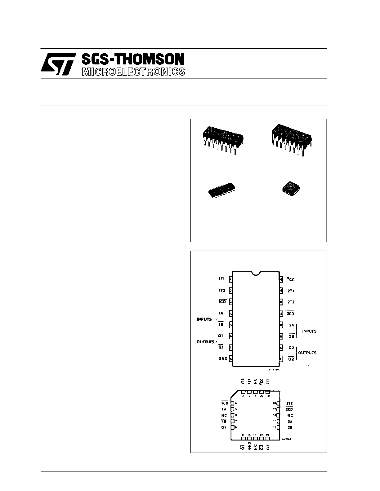
PIN CONNECTIONS(top view)
NC =
No Internal
Connection
October 1993
1/14
M54/M74HC4538
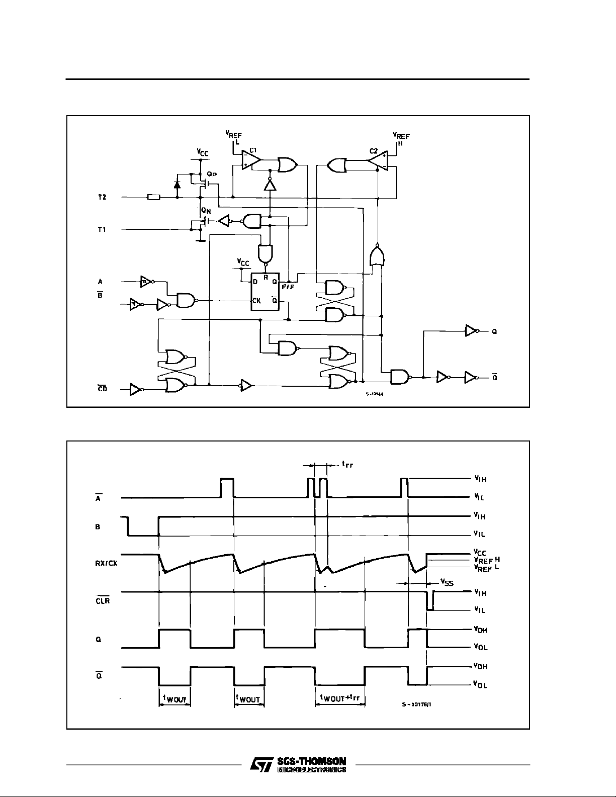
SYSTEM DIAGRAM
TIMING CHART
2/14
BLOCK DIAGRAM
M54/M74HC4538
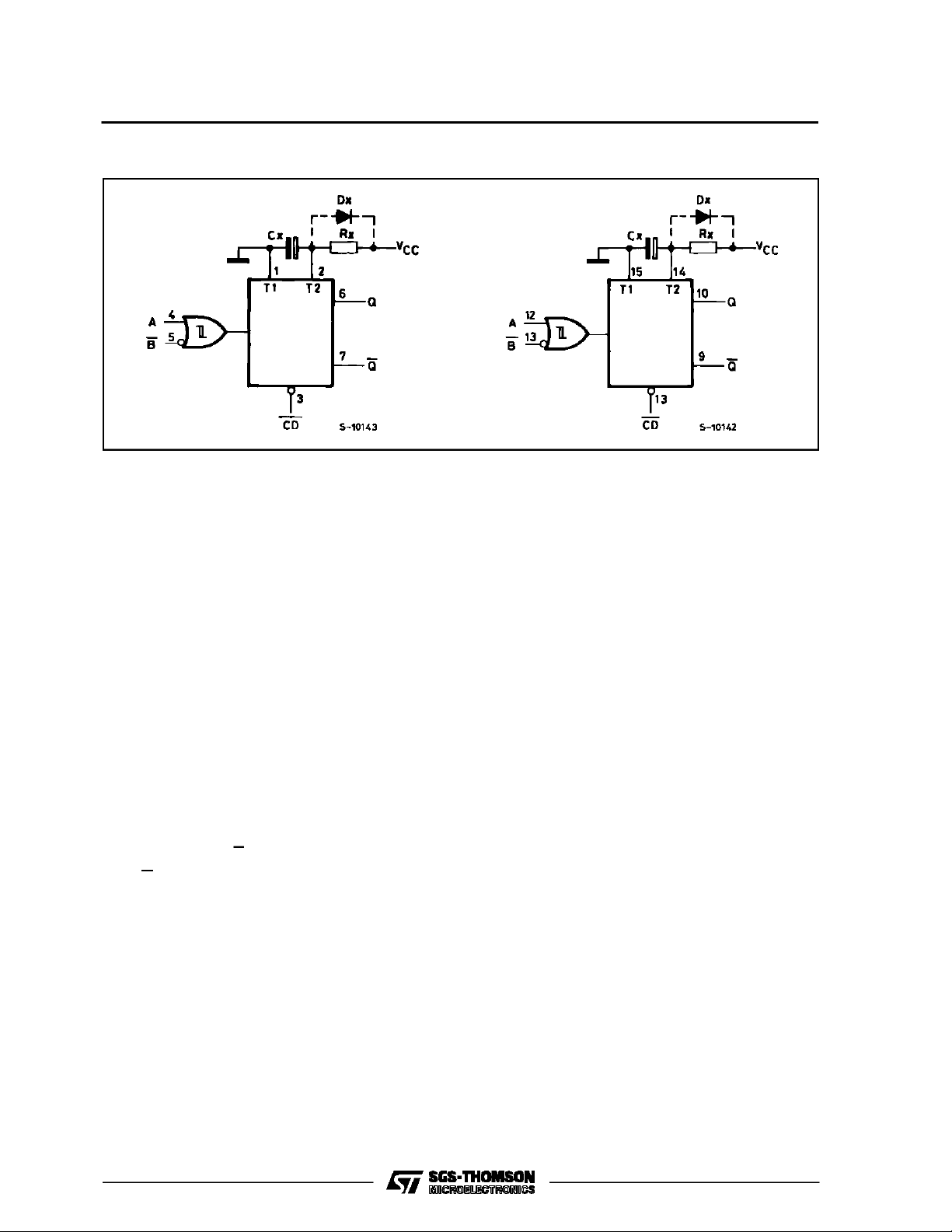
Notes : 1. Cx, Rx, Dx areexternal components.
2. Dx isa clamping diode.
3. The external capacitor is chargedto VCCinthe stand-by state, i.e. no trigger.When the supply voltage is turned off Cx is discharged
mainlythrough aninternalparasitic diode(seefigures). IfCxissufficiently largeandVCCdecreases rapidy, therewillbesomepossibility
of damaging theI.C.witha surgecurrentor latch-up. If the voltagesupplyfiltercapacitor is large enough andVCCdecrease slowly,
thesurgecurrent is automatically limitedand damage the I.C.is avoided.Themaximumforward currentof the parasitic diodeis approximately 20mA.In cases whereCx is largethe time takenfor the supply voltage to fallto 0.4VCCcan be calculated as follows :
tf≥ (VCC–0.7) ⋅ Cx/20mA
In cases where tfistooshortan externalchamping diode is requiredto protectthe I.C. from the surgecurrent.
FUNCTIONAL DESCRIPTION
STAND-BY STATE
The external capacitor, Cx, is fully charged to V
CC
inthe stand-bystate.Hence, beforetriggering, transistorQp andQn (connected totheRx/Cxnode)are
bothturnedoff.Thetwo comparatorsthatcontrolthe
timing and the two reference voltage sources stop
operating. The total supply current is therefore only
leakage current.
TRIGGEROPERATION
Triggering occurs when :
1 st)A is ”low” and B has a falling edge ;
2 nd) B is ”high” and A has a risingedge;
After the multivibrator has been retriggered com-
paratorC1 and C2 start operating and Qn isturned
on. Cx then discharges throughQn.The voltage at
the node Rx/Cx external falls.
Whenit reaches V
theoutputof comparator C1
REFL
becomeslow. Thisin turn resets theflip-flop andQn
is turnedoff.
At this point C1 stops functioning but C2 continues
tooperate.ThevoltageatR/Cexternalbeginstorise
witha timeconstant setbytheexternal components
Rx, Cx.
Triggering themultivibratorcausesQtogohigh after
internal delay dueto the flip-flop and thegate. Qremains high until the voltage at R/C external rises
againto V
. Atthis pointC2outputgoeslow and
REFH
G goes low. C2 stops operating. That means that
aftertriggering whenthe voltageat R/Cexternal returns to V
the multivibrator has returned to its
REFH
MONOSTABLE STATE. Inthe casewhere Rx • Cx
are large enoughand thedischarge time ofthe capacitorand thedelay timeintheI.C. can be ignored,
the width ofthe output pulse tw (out) is as follows:
t
W(OUT)
= 0.72 Cx • Rx
RE-TRIGGEROPERATION
When a second trigger pulse follows the first its ef-
fect will depend on the state of the multivibrator. If
the capacitor Cx is being charged the voltage level
ofRx/Cx externalfalls toV
againandQ remains
REFL
high i.e.the retrigger pulse arrivesin a time shorter
than the period Rx • Cx seconds, the capacitor
charging time constant. If the second trigger pulse
is veryclosetothe initialtrigger pulse itis ineffective
; i.e.,the second trigger must arrive inthe capacitor
discharge cycle to be ineffective.
Hence the minimum time fora secondtrigger to be
effective,trr (Min.) depends on VCCand Cx.
3/14
M54/M74HC4538
FUNCTIONAL DESCRIPTION (continued)
RESETOPERATION
CD isnormally high. If CD is low, the trigger is not
effective because Q output goes low and trigger
controlflip-flop is reset.
Also transistor Op is turned on and Cx is charged
quickyto VCC. Thismeans if CDinput goes low,the
IC becomeswaitingstateboth in operating andnon
operating state.
TRUTH TABLE
INPUTS OUTPUTS
ABCDQQ
H H OUTPUT ENABLE
X L H L H INHIBIT
H X H L H INHIBIT
L H OUTPUT ENABLE
X X L L H INHIBIT
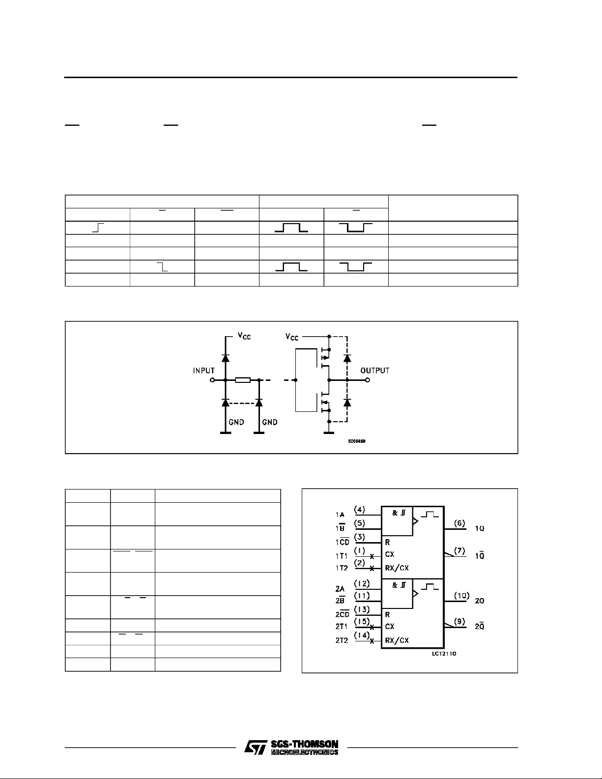
INPUT AND OUTPUT EQUIVALENT CIRCUIT
NOTE
PIN DESC RIPTION
PIN No SYMBOL NAME AND FUNCTION
1, 15 1T1, 2T1 External Capacitor
Connections
2, 14 1T2, 2T2 External Resistor/Capacitor
Connections
3, 13 1CD, 2CD Direct Reset Inputs (Active
LOW)
4, 12 1A, 2A Trigger Inputs (LOW to
HIGH, Edge-Triggered)
5, 11 1B, 2B Trigger Inputs (HIGH to
LOW, Edge-Triggered)
6, 10 Q1, Q2 Pulse Outputs
7, 9 Q1, Q2 Complementary Pulse Outputs
8 GND Ground (0V)
16 V
4/14
CC
Positive Supply Voltage
IEC LOGIC SYMBOL
M54/M74HC4538
ABSOLU TE M AXIMU M R AT INGS
Symbol Parameter Value Unit
V
CC
V
V
O
I
IK
I
OK
I
O
I
or I
CC
P
D
T
stg
T
AbsoluteMaximumRatingsarethose values beyondwhichdamage tothedevice mayoccur. Functionaloperationunder these conditionisnotimplied.
(*)500 mW: ≅ 65oC derateto 300 mWby 10mW/oC: 65oCto85oC
RECO MM ENDED OPERAT I N G CO NDI TIONS
Symbol Parameter Value Unit
V
CC
V
I
V
O
T
op
t
r,tf
C
X
R
X
(*)The maximumallowable values ofCx andRx area function of leakage of capacitor Cx, the leakageof deviceand leakagedue to the board
layoutand surface resistance. Susceptibility to externallyinduced noise may occur forRx > 1MΩ
Supply Voltage -0.5 to +7 V
DC Input Voltage -0.5 to VCC+ 0.5 V
I
DC Output Voltage -0.5 to VCC+ 0.5 V
DC Input Diode Current ± 20 mA
DC Output Diode Current ± 20 mA
DC Output Source Sink Current Per Output Pin ± 25 mA
DC VCCor Ground Current ± 50 mA
GND
Power Dissipation 500 (*) mW
Storage Temperature -65 to +150
Lead Temperature (10sec) 300
L
Supply Voltage 2 to 6 V
Input Voltage 0 to V
Output Voltage 0 to V
Operating Temperature: M54HC Series
M74HC Series
CC
CC
-55 to +125
-40 to +85
Input Rise and Fall Time (CLR only) VCC= 2 V 0 to 1000
V
= 4.5 V 0 to 500
CC
V
= 6 V 0 to 400
CC
External Capacitor NO LIMITATION (*)
External Resistor VCC≤ 3 V 5K to 1M (*)
V
>3V 1Kto1M(*)
CC
o
o
o
o
ns
C
C
V
V
C
C
Ω
5/14

M54/M74HC4538
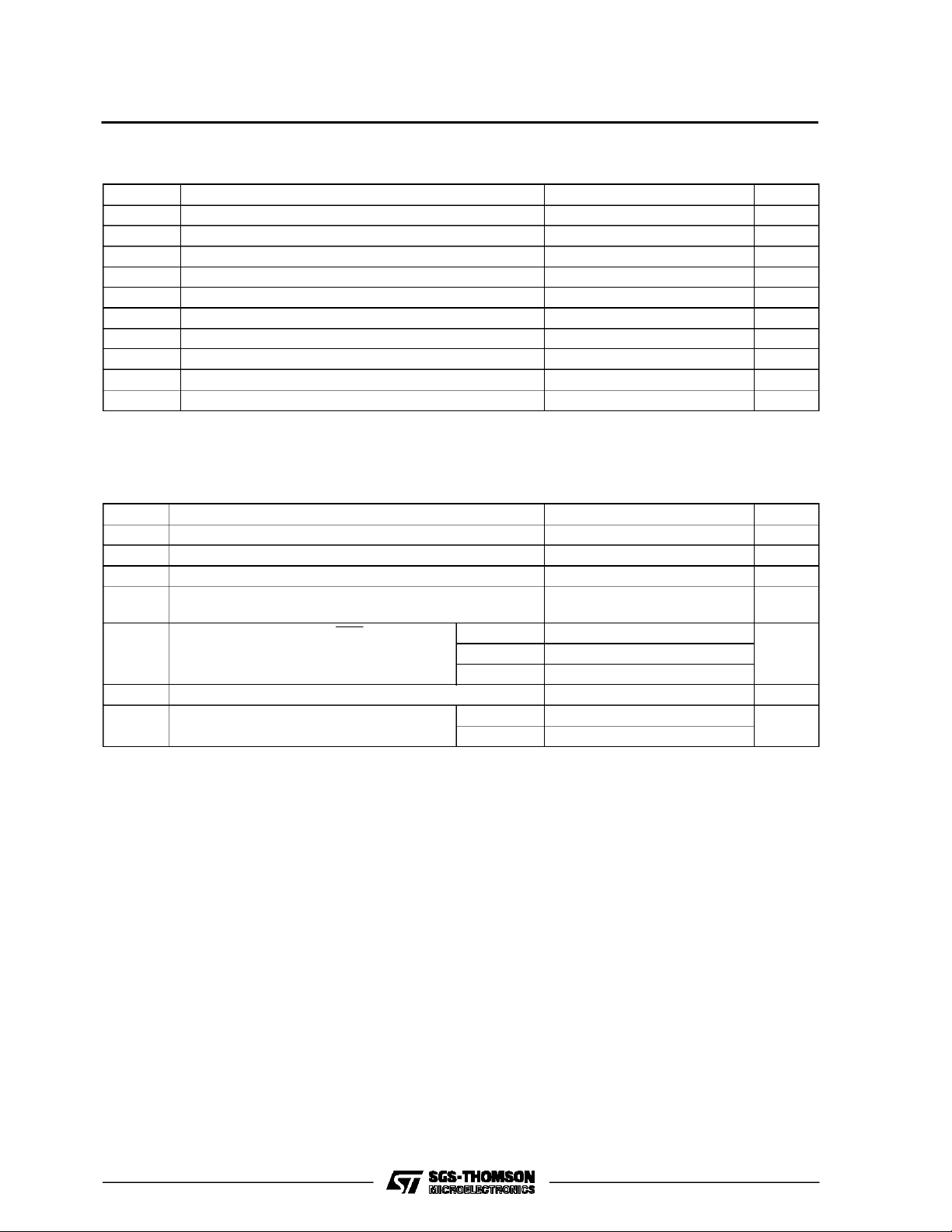
DC SPECIFICATIONS
Symbol Parameter
V
V
V
V
I
I
High Level Input
IH
Voltage
Low Level Input
IL
Voltage
High Level
OH
Output Voltage
Low Level Output
OL
Voltage
I
Input Leakage
I
Current
Input Leakage
I
I
Current
Quiescent Supply
CC
Current
Quiescent Supply
CC
Current
Test Conditions Value
V
(V)
CC
=25oC
A
54HC and 74HC
Min. Typ. Max. Min. Max. Min. Max.
-40 to 85oC
74HC
-55 to 125oC
54HC
Unit
T
2.0 1.5 1.5 1.5
4.5 3.15 3.15 3.15
6.0 4.2 4.2 4.2
2.0 0.5 0.5 0.5
4.5 1.35 1.35 1.35
6.0 1.8 1.8 1.8
2.0
4.5 4.4 4.5 4.4 4.4
6.0 5.9 6.0 5.9 5.9
4.5 I
6.0 I
2.0
4.5 0.0 0.1 0.1 0.1
6.0 0.0 0.1 0.1 0.1
4.5 I
6.0 I
6.0
6.0
=
V
I
IO=-20 µA
V
IH
or
V
IL
=-4.0 mA 4.18 4.31 4.13 4.10
O
=-5.2 mA 5.68 5.8 5.63 5.60
O
V
=
I
IO=20µA
V
IH
or
V
IL
= 4.0 mA 0.17 0.26 0.37 0.40
O
= 5.2 mA 0.18 0.26 0.37 0.40
O
VI=VCCor GND ±0.1 ±1 ±1 µA
V
I=VCC
or GND
Rext/Cext
1.9 2.0 1.9 1.9
0.0 0.1 0.1 0.1
±0.1 ±1 ±1 µA
6.0 VI=VCCor GND 4 40 80 µA
2.0 VI=VCCor GND
4.5 0.2 0.3 0.4 mA
6.0 0.3 0.6 0.8 mA
pins 2, 14
VI=VCC/2
40 120 160 µA
V
V
V
V
6/14

M54/M74HC4538
AC ELECTRICAL CHARACTERISTICS (CL=50pF,Inputtr=tf=6ns)
Test Conditions Value
T
=25oC
Symbol Parameter
t
t
TLH
THL
Output Transition
Time
V
CC
(V)
2.0 30 75 95 110
4.5 8151922
A
54HC and 74HC
Min. Typ. Max. Min. Max. Min. Max.
6.0 7131619
t
PLH
t
PHL
t
PLH
t
PHL
t
WOUT
Propagation
Delay Time
(A, B - Q, Q)
Propagation
Delay Time
(CD - Q, Q)
Output Pulse
Width
2.0 120 250 315 375
4.5 30 50 63 75
6.0 25 43 54 64
2.0 100 195 245 295
4.5 25 39 49 59
6.0 20 33 42 50
2.0
4.5 R
6.0 R
2.0
4.5 69 77 85 69 85 69 85
RX=5KΩ 540 1200 1500 1800
CX=0
C
=1KΩ 180 250 320 375
X
=1KΩ 150 200 260 320
X
= 0.01 µF
X
70 83 96 70 96 70 96
RX= 10KΩ
6.0 69 77 85 69 85 69 85
2.0
4.5 0.67 0.73 0.77 0.67 0.77 0.67 0.8
C
= 0.1 µF
X
RX= 10KΩ
0.67 0.75 0.83 0.67 0.83 0.67 0.9
6.0 0.67 0.73 0.77 0.67 0.77 0.67 0.8
∆t
WOUT
Output Pulse
±1
Width Error
Between Circuits
(In same pack)
t
W(H)
t
W(L)
t
W(L)
t
REM
Minimum Pulse
Width
(CLOCK)
Minimum Pulse
Width
(CLEAR)
Minimum Clear
Removal Time
2.0 30 75 95 110
4.5 8151922
6.0 7131619
2.0 30 75 95 110
4.5 8151922
6.0 7131619
2.0 0151520
4.5 0 5 5 7
6.0 0 5 5
t
s
Minimum
Retrigger Time
2.0
4.5 92
= 0.1 µF
C
X
RX=1KΩ
380 6
6.0 72
2.0
4.5 1.4
= 0.01 µF
C
X
RX=1KΩ
6
6.0 1.2
C
C
PD
Input Capacitance 5 10 10 10 pF
IN
(*) Power Dissipation
70
Capacitance
(*) CPDisdefined as the value ofthe IC’sinternal equivalent capacitance which is calculated from theoperatingcurrent consumption withoutload.
(RefertoTest Circuit). Average operting current canbeobtainedbythefollowingequation. ICC(opr) =CPD•VCC•fIN+ICC‘•Duty/100+ ICC/2(percircuit)
(ICC‘ = ActiveSupply Current)
(Duty= %))
-40 to 85oC
74HC
-55 to 125oC
54HC
Unit
ns
ns
ns
ns
µs
ms
%
ns
ns
ns
ns
µs
pF
7/14

M54/M74HC4538
TEST CIRCUIT ICC(Opr.)
INPUT WAVEFORMIS THE SAME AS THAT IN CASEOF
SWITCHINGCHARACTERISTICSTEST.
t
- Cx Characteristics (Typ). trr-VCCCharacteristics (Typ).
WOUT
Output PulseWidth Constant K= SupplyVoltage.
8/14

SWITCHING CHARACTERISTICS TEST WAVEFORM
M54/M74HC4538
9/14

M54/M74HC4538
Plastic DIP16 (0.25) MECHANICAL DATA
DIM.
MIN. TYP. MAX. MIN. TYP. MAX.
a1 0.51 0.020
B 0.77 1.65 0.030 0.065
b 0.5 0.020
b1 0.25 0.010
D 20 0.787
E 8.5 0.335
e 2.54 0.100
e3 17.78 0.700
F 7.1 0.280
I 5.1 0.201
L 3.3 0.130
Z 1.27 0.050
mm inch
10/14
P001C

Ceramic DIP16/1 MECHANICAL DATA
M54/M74HC4538
DIM.
MIN. TYP. MAX. MIN. TYP. MAX.
A 20 0.787
B 7 0.276
D 3.3 0.130
E 0.38 0.015
e3 17.78 0.700
F 2.29 2.79 0.090 0.110
G 0.4 0.55 0.016 0.022
H 1.17 1.52 0.046 0.060
L 0.22 0.31 0.009 0.012
M 0.51 1.27 0.020 0.050
N 10.3 0.406
P 7.8 8.05 0.307 0.317
Q 5.08 0.200
mm inch
P053D
11/14

M54/M74HC4538
SO16 (Narrow) MECHANICAL DATA
DIM.
MIN. TYP. MAX. MIN. TYP. MAX.
A 1.75 0.068
a1 0.1 0.2 0.004 0.007
a2 1.65 0.064
b 0.35 0.46 0.013 0.018
b1 0.19 0.25 0.007 0.010
C 0.5 0.019
c1 45° (typ.)
D 9.8 10 0.385 0.393
E 5.8 6.2 0.228 0.244
e 1.27 0.050
e3 8.89 0.350
F 3.8 4.0 0.149 0.157
G 4.6 5.3 0.181 0.208
L 0.5 1.27 0.019 0.050
M 0.62 0.024
S8°(max.)
mm inch
12/14
P013H

PLCC20 MECHANICAL DATA
M54/M74HC4538
DIM.
MIN. TYP. MAX. MIN. TYP. MAX.
A 9.78 10.03 0.385 0.395
B 8.89 9.04 0.350 0.356
D 4.2 4.57 0.165 0.180
d1 2.54 0.100
d2 0.56 0.022
E 7.37 8.38 0.290 0.330
e 1.27 0.050
e3 5.08 0.200
F 0.38 0.015
G 0.101 0.004
M 1.27 0.050
M1 1.14 0.045
mm inch
P027A
13/14

M54/M74HC4538
Information furnishedis believed to be accurate and reliable. However, SGS-THOMSON Microelectronicsassumes no responsability for the
consequences of useof suchinformation nor for any infringement of patents or other rights of third parties which may results from its use. No
license is granted byimplication or otherwiseunder any patentor patentrights ofSGS-THOMSON Microelectronics.Specificationsmentioned
in this publication are subjectto changewithout notice. This publication supersedes andreplaces all information previouslysupplied.
SGS-THOMSON Microelectronicsproducts are not authorized foruse ascritical componentsin life supportdevices or systems without express
written approval of SGS-THOMSON Microelectonics.
1994SGS-THOMSON Microelectronics- All Rights Reserved
Australia -Brazil - France - Germany - Hong Kong - Italy - Japan - Korea - Malaysia - Malta -Morocco - The Netherlands-
Singapore -Spain - Sweden- Switzerland - Taiwan - Thailand- UnitedKingdom - U.S.A
SGS-THOMSON Microelectronics GROUP OFCOMPANIES
14/14
 Loading...