

SGS-THOMSON M54HCT86, M74HCT86 Technical data

M54HCT86
.HIGH SPEED
.tPD = 15 ns (TYP.) AT VCC = 5 V LOW POWER DISSIPATION
.ICC = 1 μA (MAX.) AT TA = 25 °C COMPATIBLE WITH TTL OUTPUTS
.VIH = 2V (MIN.) VIL = 0.8V (MAX)
OUTPUT DRIVE CAPABILITY
.10 LSTTL LOADS
SYMMETRICAL OUTPUT IMPEDANCE
. IOH = IOL = 4 mA (MIN.) BALANCED PROPAGATION DELAYS
.tPLH = tPHL
PIN AND FUNCTION COMPATIBLE WITH 54/74LS86
DESCRIPTION
The M54/74HCT86 is a high speed CMOS QUAD EXCLUSIVE OR GATE fabricated in silicon gate C2MOS technology.
It has the same high speed performance of LSTTL combined with true CMOS low power consumption. Input and output buffer are installed, which enables high noise immunity and stable output.
All inputs are equipped with protection circuits against static discharge and transient excess voltage.This integrated circuit has input and output characteristics that are fully compatible with 54/74 LSTTL logic families. M54/74HCT devices are designed to directly interface HSC2MOS systems with TTL and NMOS components. They are also plug in replacements for LSTTL devices giving a reduction of power consumption.
INPUT AND OUTPUT EQUIVALENT CIRCUIT
M54HCT86
M74HCT86
QUAD EXCLUSIVE OR GATE
B1R |
F1R |
(Plastic Package) |
(Ceramic Package) |
M1R |
C1R |
(Micro Package) |
(Chip Carrier) |
ORDER CODES : |
|
M54HCT86F1R |
M74HCT86M1R |
M74HCT86B1R |
M74HCT86C1R |
PIN CONNECTIONS (top view)
NC =
No Internal
Connection
February 1993 |
1/9 |

M54/M74HCT86
TRUTH TABLE |
|
IEC LOGIC SYMBOL |
|
A |
|
B |
Y |
L |
|
L |
L |
L |
|
H |
H |
H |
|
L |
H |
H |
|
H |
L |
PIN DESCRIPTION |
|
|
|
PIN No |
SYMBOL |
|
NAME AND FUNCTION |
1, 4, 9, 12 |
1A to 4A |
|
Data Inputs |
2, 5, 10, 13 |
1B to 4B |
|
Data Inputs |
3, 6, 8, 11 |
1Y to 4Y |
|
Data Outputs |
7 |
GND |
|
Ground (0V) |
14 |
VCC |
|
Positive Supply Voltage |
SCHEMATIC CIRCUIT (Per Gate)
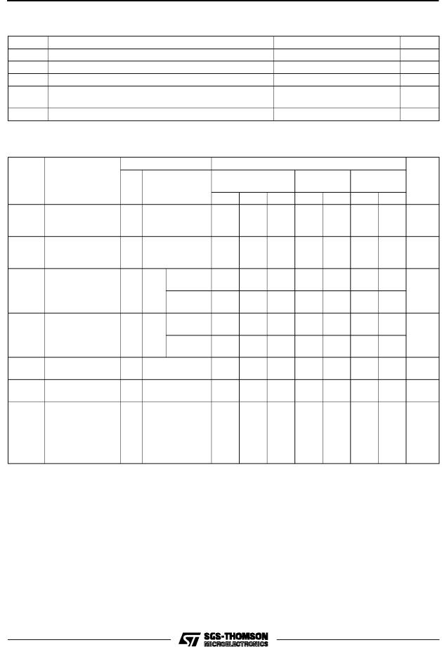
ABSOLUTE MAXIMUM RATINGS
Symbol |
Parameter |
Value |
Unit |
VCC |
Supply Voltage |
-0.5 to +7 |
V |
VI |
DC Input Voltage |
-0.5 to VCC + 0.5 |
V |
VO |
DC Output Voltage |
-0.5 to VCC + 0.5 |
V |
IIK |
DC Input Diode Current |
± 20 |
mA |
IOK |
DC Output Diode Current |
± 20 |
mA |
IO |
DC Output Source Sink Current Per Output Pin |
± 25 |
mA |
ICC or IGND |
DC VCC or Ground Current |
± 50 |
mA |
PD |
Power Dissipation |
500 (*) |
mW |
Tstg |
Storage Temperature |
-65 to +150 |
oC |
TL |
Lead Temperature (10 sec) |
300 |
oC |
Absolute Maximum Ratings are those values beyond which damage to the device may occur. Functional operation under these condition isnotimplied.
(*) 500 mW: 65 oC derate to 300 mW by 10mW/oC: 65 oC to 85 oC
2/9
|
|
|
|
|
|
|
|
|
M54/M74HCT86 |
|
RECOMMENDED OPERATING CONDITIONS |
|
|
|
|
|
|||||
Symbol |
|
|
Parameter |
|
|
|
Value |
|
Unit |
|
VCC |
Supply Voltage |
|
|
|
|
|
|
4.5 to 5.5 |
|
V |
VI |
Input Voltage |
|
|
|
|
|
|
0 to VCC |
|
V |
VO |
Output Voltage |
|
|
|
|
|
|
0 to VCC |
|
V |
Top |
Operating Temperature: M54HC Series |
|
|
|
-55 to +125 |
oC |
||||
|
|
|
M74HC Series |
|
|
|
-40 to +85 |
|
oC |
|
tr, tf |
Input Rise and Fall Time (VCC = 4.5 to 5.5V) |
|
|
|
0 to 500 |
|
ns |
|||
DC SPECIFICATIONS |
|
|
|
|
|
|
|
|
|
|
|
|
Test Conditions |
|
|
|
Value |
|
|
||
Symbol |
Parameter |
VCC |
|
|
TA = 25 oC |
-40 to 85 oC -55 to 125 oC |
Unit |
|||
|
|
|
|
54HC and 74HC |
74HC |
54HC |
|
|||
|
|
(V) |
|
|
|
|||||
|
|
|
|
Min. Typ. Max. Min. Max. Min. Max. |
|
|||||
|
|
|
|
|
|
|||||
VIH |
High Level Input |
4.5 |
|
|
2.0 |
|
|
2.0 |
2.0 |
V |
|
Voltage |
to |
|
|
|
|
|
|
|
|
|
|
5.5 |
|
|
|
|
|
|
|
|
VIL |
Low Level Input |
4.5 |
|
|
|
|
0.8 |
0.8 |
0.8 |
V |
|
Voltage |
to |
|
|
|
|
|
|
|
|
|
|
5.5 |
|
|
|
|
|
|
|
|
VOH |
High Level |
|
VI = |
IO=-20 μA |
4.4 |
4.5 |
|
4.4 |
4.4 |
|
|
Output Voltage |
4.5 |
VIH |
|
|
|
|
|
|
V |
|
|
or |
IO=-4.0 mA |
4.18 |
4.31 |
|
4.13 |
4.10 |
||
|
|
|
|
|
||||||
|
|
|
VIL |
|
|
|||||
|
|
|
|
|
|
|
|
|
|
|
VOL |
Low Level Output |
|
VI = |
IO= 20 μA |
|
0.0 |
0.1 |
0.1 |
0.1 |
|
|
Voltage |
4.5 |
VIH |
|
|
|
|
|
|
V |
|
|
or |
IO= 4.0 mA |
|
0.17 |
0.26 |
0.33 |
0.4 |
||
|
|
|
|
|
||||||
|
|
|
VIL |
|
|
|||||
|
|
|
|
|
|
|
|
|
|
|
II |
Input Leakage |
5.5 |
VI = VCC or GND |
|
|
±0.1 |
±1 |
±1 |
μA |
|
|
Current |
|
|
|
|
|
|
|
|
|
|
|
|
|
|
|
|
|
|
|
|
ICC |
Quiescent Supply |
5.5 |
VI = VCC or GND |
|
|
1 |
10 |
20 |
μA |
|
|
Current |
|
|
|
|
|
|
|
|
|
ICC |
Additional worst |
5.5 |
Per Input pin |
|
|
2.0 |
2.9 |
3.0 |
mA |
|
|
case supply |
|
VI = 0.5V or |
|
|
|
|
|
|
|
|
current |
|
VI = 2.4V |
|
|
|
|
|
|
|
|
|
|
Other Inputs at |
|
|
|
|
|
|
|
VCC or GND
IO= 0
3/9
 Loading...