

SGS-THOMSON M54HCT00, M74HCT00 Technical data

查询M54HCT00供应商
.HIGH SPEED
tPD= 12 ns(TYP.) AT VCC=5V
.LOWPOWER DISSIPATION
ICC=1µA(MAX.) AT TA=25°C
.COMPATIBLE WITH TTL OUTPUTS
VIH= 2V (MIN.) VIL= 0.8V(MAX)
.OUTPUTS DRIVE CAPABILITY
10 LSTTL LOADS
.BALANCEDPROPAGATION DELAYS
t
PLH=tPHL
.PIN AND FUNCTION COMPATIBLE
WITH 54/74LS00
.SYMMETRICALOUTPUT IMPEDANCE
IOH =IOL= 4 mA (MIN.)
DESCRIPTION
The M54/74HCT00 is a high speed CMOS QUAD
2-INPUT NAND GATE fabricated in silicon gate
C2MOStechnology.It hasthesamehighspeedperformance of LSTTL combined with true CMOS low
power consumption. The internal circuit is composedof 3 stages including bufferoutput,which enables high noise immunity and stable output. All
inputs are equipped with protection circuits against
staticdischarge and transient excess voltage.
This integrated circuit has input and outputcharacteristicsthat are fully compatible with 54/74 LSTTL
logic families. M54/74HC devices are designed to
directly interface HSC2MOSsystems with TTL and
NMOS components. They are also plug in replacements for LSTTL devices giving a reduction of
powerconsumption.
M54HCT00
M74HCT00
QUAD 2-INPUT NAND GATE
B1R
(PlasticPackage)
M1R
(MicroPackage)
ORDER CODES :
M54HC T00F1R M74H CT00M1R
M74HC T00B1R M74HCT00C1R
PIN CONNECTIONS (top view)
F1R
(CeramicPackage)
C1R
(Chip Carrier)
INPUT AND OUTPUT EQUIVALENT CIRCUIT
February 1993
NC =
No Internal
Connection
1/9

M54/M74HCT00
TRUTH TABLE
ABY
LLH
LHH
HLH
HHL
PIN DESCRIPTION
PIN No SYMBOL NAME AND FUNCTION
1, 4, 9, 12 1A to 4A Data Inputs
2, 5, 10, 13 1B to 4B Data Inputs
3, 6, 8, 11 1Y to 4Y Data Outputs
7 GND Ground (0V)
14 V
CC
Positive Supply Voltage
LOGI C DI AG RAM
IEC LOGIC SYMBOL
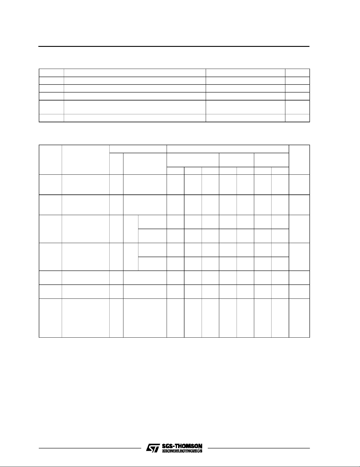
ABSOLU TE M AXIMU M R AT INGS
Symbol Parameter Value Unit
V
CC
V
V
O
I
IK
I
OK
I
O
or I
I
CC
P
D
T
stg
T
L
AbsoluteMaximumRatingsarethose values beyondwhichdamagetothedevice mayoccur. Functionaloperationunder theseconditionisnotimplied.
(*)500 mW:≅ 65oC derateto 300 mWby 10mW/oC: 65oCto85oC
2/9
Supply Voltage -0.5 to +7 V
DC Input Voltage -0.5 to VCC+ 0.5 V
I
DC Output Voltage -0.5 to VCC+ 0.5 V
DC Input Diode Current ± 20 mA
DC Output Diode Current ± 20 mA
DC Output Source Sink Current Per Output Pin ± 25 mA
DC VCCor Ground Current ± 50 mA
GND
Power Dissipation 500 (*) mW
Storage Temperature -65 to +150
Lead Temperature (10 sec) 300
o
C
o
C
M54/M74HCT00
RECO MM ENDED OPERATING C ONDI TI O NS
Symbol Parameter Value Unit
V
V
V
T
t
r,tf
DC SPECIFICATIONS
Symbol Parameter
V
V
V
OH
V
OL
I
I
CC
∆I
Supply Voltage 4.5 to 5.5 V
CC
Input Voltage 0 to V
I
Output Voltage 0 to V
O
Operating Temperature: M54HC Series
op
M74HC Series
CC
CC
-55 to +125
-40 to +85
Input Rise and Fall Time (VCC= 4.5 to 5.5V) 0 to 500 ns
Test Conditions Value
T
High Level Input
IH
Voltage
V
(V)
4.5
=25oC
CC
A
54HC and 74HC
Min. Typ. Max. Min. Max. Min. Max.
2.0 2.0 2.0 V
to
-40 to 85oC
74HC
-55 to 125oC
5.5
Low Level Input
IL
Voltage
4.5
to
0.8 0.8 0.8 V
5.5
High Level
Output Voltage
Low Level Output
Voltage
Input Leakage
I
Current
Quiescent Supply
VI=
IO=-20 µA 4.4 4.5 4.4 4.4
V
IH
4.5
or
I
=-4.0 mA 4.18 4.31 4.13 4.10
O
V
IL
VI=
IO=20µA 0.0 0.1 0.1 0.1
V
IH
4.5
or
I
= 4.0 mA 0.17 0.26 0.33 0.40
O
V
IL
VI=VCCor GND ±0.1 ±1 ±1 µA
5.5
5.5 VI=VCCor GND 1 10 20 µA
Current
Additional worst
CC
case supply
current
5.5 Per Input pin
V
= 0.5V or
I
VI= 2.4V
2.0 2.9 3.0 mA
Other Inputs at
VCCor GND
IO=0
54HC
V
V
o
C
o
C
Unit
V
V
3/9
 Loading...