

查询M54HC4351供应商
M54HC4351/52/53
M74HC4351/52/53
ANALOG MULTIPLEXER/DEMULTIPLEXER WITHADDRE SS LATCH:
SIN GLE 8CH ANN EL, DUAL4C HAN NEL, TRIPLE2 CH ANNEL
.LOGIC LEVEL TRANSLATION TO ENABLE 5V
LOGIC SIGNAL TO COMMUNICATE WITH
±5V ANALOGSIGNAL
.WIDE OPERATINGVOLTAGERANGE
(VCC-VEE) 2V TO 12V
.LOW ”ON” RESISTANCE:
70Ω TYP.(VCC-VEE= 4.5 V)
50Ω TYP.(VCC-VEE=9V)
.WIDEANALOGINPUTVOLTAGERANGE:±6V
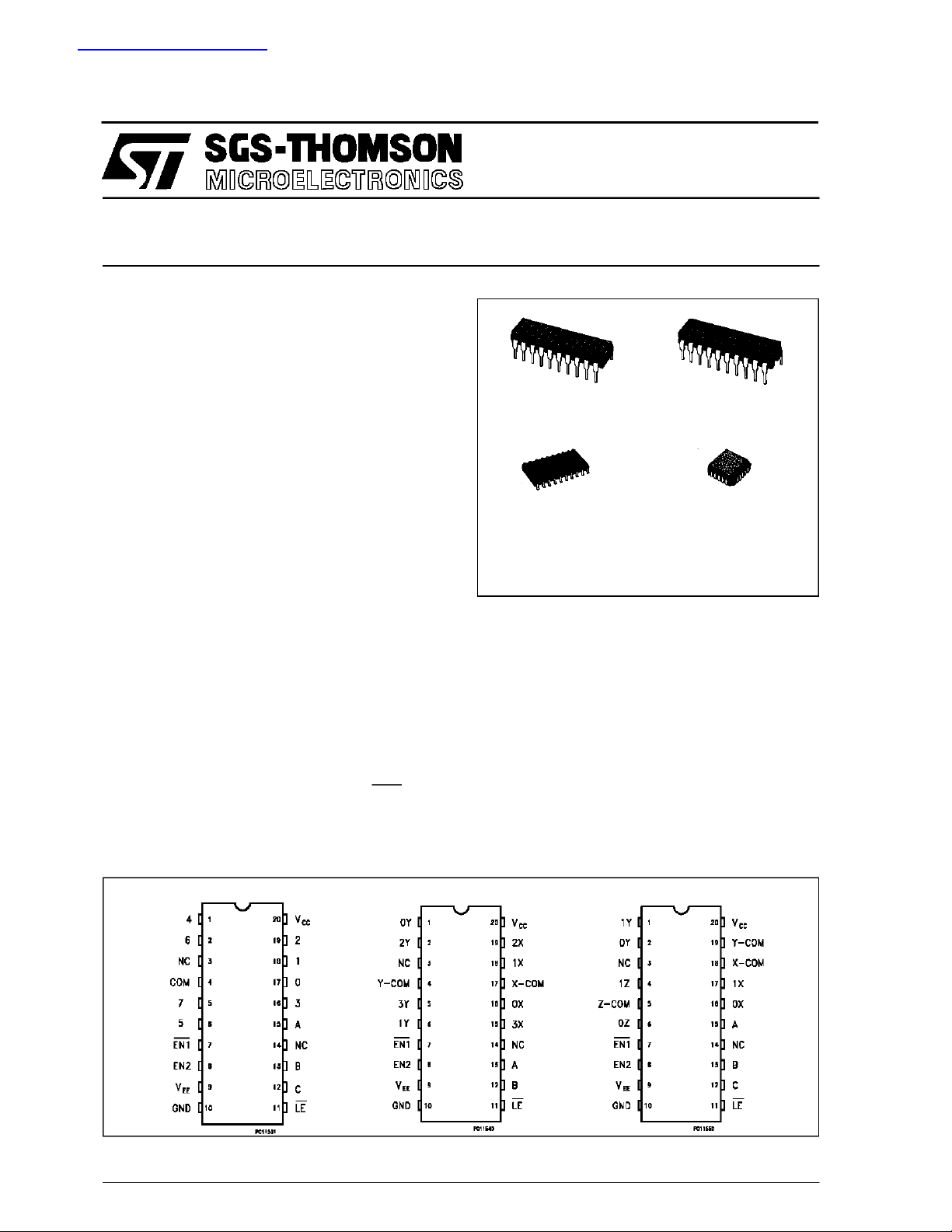
B1R
(PlasticPackage)
F1R
(CeramicPackage)
.FAST SWITCHING
.LOW CROSSTALK BETWEEN SWITCHES
.HIGH ON/OFF OUTPUTVOLTAGERATIO
.LOW SINE WAVEDISTORTION:
0.02% (TYP.) AT VCC-VEE=9V
.HIGH NOISEIMMUNITY
V
NIH=VNIL
= 28% VCC(MIN.)
.LOW POWER DISSIPATION
ICC=4µA (MAX)AT TA=25oC
M1R
(MicroPackage)
ORDER CODES :
M54HC XXXX F 1R M74H CX XXXM1R
M74HC XXXX B1R M74HCXXXXC1 R
C1R
(Chip Carrier)
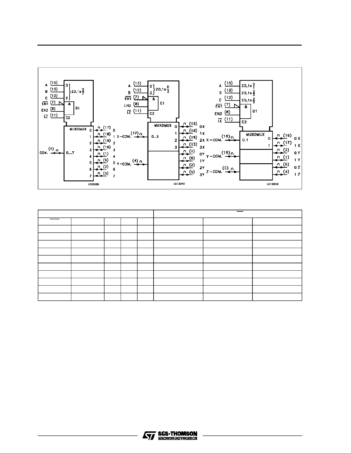
DESCRIPTION
These devices are analog multiplexer
demultiplexers in high speed silicon gate C2MOS
technology. Theseanalog switchesarebidirectional
and digitally controlled. A built-in level shifting is
included to allowthema controlinput range of up to
± 6V (peak) for an analog signalwith digital control
signalof 0 to 6V.
VEEsupply pin is providedfor analoginput signals.
They have two enable inputs to enable all the
switches when high (EN2) or low (EN1). For
operation asa digitalmultiplexer/demultiplexer, V
is connected toGND.
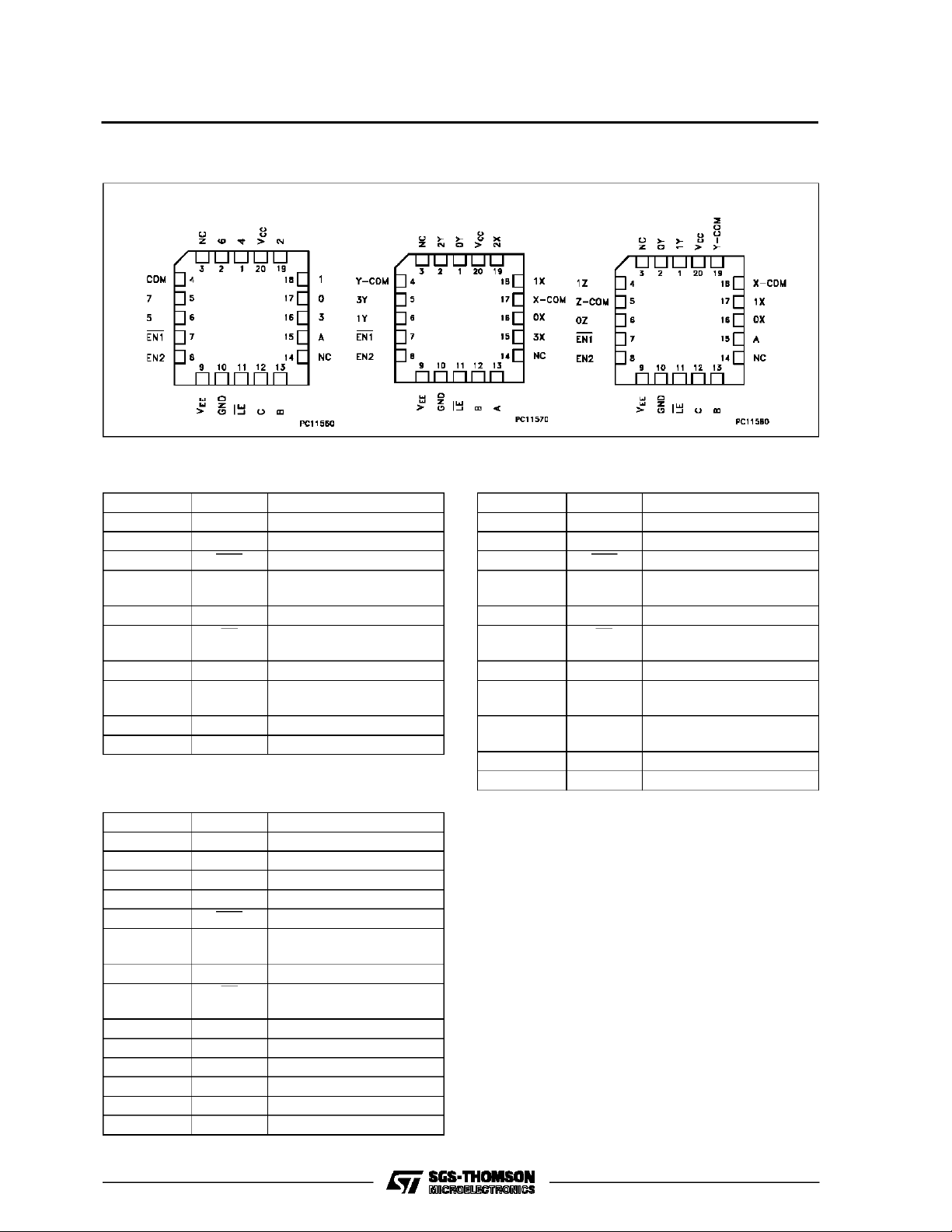
PIN CONNECTION (top view)
EE
The HC4351 is a single 8 channel multiplexer
demultiplexer havingthree binary controlinputs A,
B and C to select 1 of 8 to be turned on, and
connected to the output.
The HC4352 has a pair of four channel multiplexer
demultiplexer havingtwocontrolinputsA andBthat
selectone offour channel of the two sections.
The HC4353 is a triple two channel multiplexer
demultiplexer havingthree separate digitalcontrol
inputs A, B and C toselect independently one of a
pairof channles.
HC4353HC435 2HC4351
November1993
1/16
M54/M74HC4351/4352/4353
CHIP CARRIER
HC4353HC435 2HC4351
PIN DESCRIPTION (HC4351)
PIN No SYMBOL NAME AND FUNCTION
4 COM Common
3, 14 NC Not Connected
7 EN1 Enable Input (Active LOW)
8 EN2 Enable Input (Active
HIGH)
9V
EE
Negative Supply Voltage
11 LE Latch Enable Input
(Active LOW)
15, 13, 12 A, B, C Select Inputs
17, 18, 19,
0 to 7 Independent Input/Outputs
16, 1, 6, 2, 5
10 GND Ground (0V)
20 V
CC
Positive Supply Voltage
PIN DESCRIPTION (HC4353)
PIN No SYMBOL NAME AND FUNCTION
1, 2 0Y 1Y Independent Input/Outputs
5 Z COM Common Output/Inputs
6, 4 0Z, 1Z Independent Input/Outputs
3, 14 NC Not Connected
7 EN1 Enable Input (Active LOW)
8 EN2 Enable Input (Active
HIGH)
9V
EE
11 LE Latch Enable Input
15, 13, 12 A, B, C Select Inputs
16, 17 0X, 1X Independent Input/Outputs
18 X COM Common Output/Inputs
19 Y COM Common Output/Inputs
10 GND Ground (0V)
20 V
CC
Negative Supply Voltage
(Active LOW)
Positive Supply Voltage
PIN DESCRIPTION (HC 4352)
PIN No SYMBOL NAME AND FUNCTION
1, 6, 2, 5 0Y to 3Y Independent Input/Outputs
3, 14 NC Not Connected
7 EN1 Enable Input (Active LOW)
8 EN2 Enable Input (Active
HIGH)
9V
EE
11 LE Latch Enable Input
13, 12 A, B Select Inputs
16, 18, 19,150X to 3X IndependentInput/Outputs
17, 4 X COM
Y COM
10 GND Ground (0V)
20 V
CC
Negative Supply Voltage
(Active LOW)
Common Output/Inputs
Positive Supply Voltage
2/16
IEC LOGIC SYMBOLS
TRUTH TABLE
M54/M74HC4351/4352/4353
HC435 3HC4352HC4351
CONTROL INPUTS ”ON” CHANNEL (LE = H) **
EN1 EN2 C * B A HC4351 HC4352 HC4353
L H L L L 0 0X, 0Y 0X, 0Y, 0Z
L H L L H 1 1X, 1Y 1X, 0Y, 0Z
L H L H L 2 2X, 2Y 0X, 1Y, 0Z
L H L H H 3 3X, 3Y 1X, 1Y, 0Z
L H H L L 4 - - 0X, 0Y, 1Z
L H H L H 5 - - 1X, 0Y, 1Z
L H H H L 6 - - 0X, 1Y, 1Z
L H H H H 7 - - 1X, 1Y, 1Z
H X X X X NONE NONE NONE
X L X X X NONE NONE NONE
X: DON’T CARE *: HC4351/3only
** When latchEnable is low, the Channel Selection is latched and the Channel Address Latch does not change state.
3/16
M54/M74HC4351/4352/4353
ABSOLU TE M AXI MUM RAT ING S
Symbol Parameter Value Unit
V
CC
V
CC-VEE
V
IN
V
I/O
I
IK
I
OK
I
OUT
I
or I
CC
P
T
stg
T
AbsoluteMaximumRatingsarethosevalues beyondwhichdamagetothedevicemayoccur.Functionaloperationundertheseconditionisnotimplied.
(*)500 mW: ≅ 65oC derate to300 mW by 10mW/oC: 65oCto85oC
RECO MM ENDED OPERATIN G CO NDI TIONS
Symbol Parameter Value Unit
V
CC
V
EE
V
CC-VEE
V
IN
V
I/O
T
op
t
r,tf
Supply Voltage Range -0.5 to +7 V
Supply Voltage Range -0.5 to 13 V
DC Input Voltage -0.5 to VCC+ 0.5 V
DC Switch I/O Voltage VEE- 0.5 to VCC+ 0.5 V
Input Diode Current ± 20 mA
I/O Diode Current ± 20 mA
DC Output Current ± 25 mA
DC VCCor Ground Current ± 50 mA
GND
Power Dissipation 500 (*) mW
D
Storage Temperature -65 to +150
Lead Temperature (10 sec) 300
L
Supply Voltage 2 to 6 V
Supply Voltage -6 to 0 V
Supply Voltage 2 to 12 V
Input Voltage 0 to V
DC Switch I/O Voltage VEEto V
Operating Temperature: M54HC Series
M74HC Series
CC
CC
-55 to +125
-40 to +85
Input Rise and Fall Time VCC= 2 V 0 to 1000 ns
= 4.5 V 0 to 500
V
CC
V
= 6 V 0 to 400
CC
o
C
o
C
V
V
o
C
o
C
4/16
DC SPECIFICATIONS
Symbol Parameter
V
V
R
High Level
IHC
Control Input
Voltage
Low Level Control
ILC
Input
Voltage
ON Resistance 4.5 GND VIN=V
ON
M54/M74HC4351/4352/4353
Test Conditions Value
T
=25oC
V
(V)
CC
V
(V)
EE
A
54HC and 74HC
Min. Typ. Max. Min. Max. Min. Max.
2.0 1.5 1.5 1.5
4.5 3.15 3.15 3.15
6.0 4.2 4.2 4.2
2.0 0.5 0.5 0.5
4.5 1.35 1.35 1.35
6.0 1.8 1.8 1.8
or
IHC
V
4.5 -4.5 55 120 150
6.0 -6.0 50 100 125
2.0 GND V
4.5 GND 70 150 190
4.5 -4.5 50 100 125
6.0 -6.0 45 80 100
V
I/O=VCC
V
I
≤ 2mA
I/O
IN=VIHC
V
V
I/O=VCC
V
I
≤ 2mA
I/O
ILC
to
EE
or
ILC
or
EE
85 180 225
150
-40 to 85oC
74HC
-55 to 125oC
54HC
Unit
V
V
Ω
∆R
I
Difference of ON
ON
Resistance
Between Switches
Input/Output
OFF
Leakage Current
(SWITCH OFF) 6.0 -6.0
I
Switch Input
IZ
Leakage Current
(SWITCH ON)
I
Control Input
IN
Current
I
Quiescent Supply
CC
Current
4.5 GND VIN=V
4.5 -4.5 5 12 15
6.0 -6.0 5 10 12
V
I/O=VCC
I
I/O
VOS=VCCor
IHC
V
ILC
V
EE
≤ 2mA
or
10 30 35
to
±100 ±1000 ± nA
GND
VIS= GND or
V
CC
VIN=V
ILC
VOS=VCCor
6.0 -6.0
6.0 GND
GND
V
INH=VIHC
V
IN=VCC
GND
or
6.0 GND VIN=VCCor
6.0 -6.0 8 80 160
GND
±100 ±1000 ± nA
±0.1 ±1 ±1 µA
44080µA
Ω
5/16

M54/M74HC4351/4352/4353
AC ELECTRICAL CHARACTERISTICS fo r HC4351 (CL=50pF,Inputtr=tf=6ns,GND=0V)
Test Conditions Value
=25oC
T
Symbol Parameter
Φ
Phase Difference
I/O
Between Input
and Output
V
V
CC
EE
(V)
(V)
2.0 GND 25 60 75
4.5 GND 6 12 15
6.0 GND 5 10 13
A
54HC and 74HC
Min. Typ. Max. Min. Max. Min. Max.
4.5 -4.5 4
t
t
PZL
PZH
Output Enable
Time
(E1, E2 - O)
2.0 GND RL=1KΩ 80 200 250 300
4.5 GND 20 40 50 60
6.0 GND 16 34 43 51
4.5 -4.5 18
t
t
PZL
PZH
Output Enable
Time
(LE - I/O)
2.0 GND RL=1KΩ 80 225 280 340
4.5 GND 22 45 56 68
6.0 GND 17 38 48 57
4.5 -4.5 18
t
t
PZL
PZH
Output Enable
Time
(A, B, C - I/O)
2.0 GND RL=1KΩ 75 225 280 340
4.5 GND 22 45 56 68
6.0 GND 16 38 48 57
4.5 -4.5 17
t
t
PLZ
PHZ
Output Disable
Time
(E1, E2 - O)
2.0 GND RL=1KΩ 120 275 344 415
4.5 GND 38 55 69 83
6.0 GND 33 47 59 71
4.5 -4.5 30
t
t
PLZ
PHZ
Output Disable
Time
(LE - I/O)
2.0 GND RL=1KΩ 120 275 344 415
4.5 GND 40 55 69 83
6.0 GND 35 47 59 71
4.5 -4.5 34
t
t
PLZ
PHZ
Output Disable
Time
(A, B, C - I/O)
2.0 GND RL=1KΩ 120 290 363 433
4.5 GND 40 58 73 87
6.0 GND 35 49 61 74
4.5 -4.5 35
t
W(H)
Minimum Pulse
Width (LE)
2.0 75 95 110
4.5 15 19 22
6.0 13 16 19
t
s
Minimum Set Up
Time
2.0 50 60 75
4.5 10 12 15
6.0 9 11 13
t
h
Minimum Hold
Time
2.0 5 5 5
4.5 5 5 5
6.0 5 5 5
C
C
C
C
C
PD
Input Capacitance 5 10 10 10 pF
IN
Common Terminal
IS
Capacitance
Switch Terminal
OS
Capacitance
Feed Through
IOS
Capacitance
(*) Power Dissipation
5.0 -5.0
5.0 -5.0
5.0 -5.0
5.0 GND 23
36 70 70 70
7151515
0.95 2 2 2
Capacitance
(*) CPDisdefined asthe valueof the IC’s internal equivalent capacitance which is calculated fromthe operating current consumption withoutload.
(Referto TestCircuit).Average operting current can be obtained by thefollowingequation. ICC(opr) = CPD•VCC•fIN+I
-40 to 85oC
74HC
-55 to 125oC
54HC
CC
Unit
ns
ns
ns
ns
ns
ns
ns
ns
ns
ns
pF
pF
pF
pF
6/16

M54/M74HC4351/4352/4353
AC ELECTRICAL CHARACTERISTICS fo r HC4352 (CL=50pF,Inputtr=tf=6ns,GND=0V)
Test Conditions Value
=25oC
T
Symbol Parameter
Φ
Phase Difference
I/O
Between Input
and Output
V
V
CC
EE
(V)
(V)
2.0 GND 25 60 75
4.5 GND 6 12 15
6.0 GND 5 10 13
A
54HC and 74HC
Min. Typ. Max. Min. Max. Min. Max.
4.5 -4.5 4
t
t
PZL
PZH
Output Enable
Time
(E1, E2 - O)
2.0 GND RL=1KΩ 80 200 250 300
4.5 GND 20 40 50 60
6.0 GND 16 34 43 51
4.5 -4.5 18
t
t
PZL
PZH
Output Enable
Time
(LE - I/O)
2.0 GND RL=1KΩ 80 225 280 340
4.5 GND 22 45 56 68
6.0 GND 17 38 48 57
4.5 -4.5 18
t
t
PZL
PZH
Output Enable
Time
(A, B, C - I/O)
2.0 GND RL=1KΩ 80 225 280 340
4.5 GND 22 45 56 68
6.0 GND 16 38 48 57
4.5 -4.5 17
t
t
PLZ
PHZ
Output Disable
Time
(E1, E2 - O)
2.0 GND RL=1KΩ 120 275 344 415
4.5 GND 38 55 69 83
6.0 GND 33 47 59 71
4.5 -4.5 36
t
t
PLZ
PHZ
Output Disable
Time
(LE - I/O)
2.0 GND RL=1KΩ 160 275 344 415
4.5 GND 40 55 69 83
6.0 GND 34 47 59 71
4.5 -4.5 32
t
t
PLZ
PHZ
Output Disable
Time
(A, B, C - I/O)
2.0 GND RL=1KΩ 120 275 344 415
4.5 GND 40 55 69 83
6.0 GND 35 47 59 71
4.5 -4.5 31
t
W(H)
Minimum Pulse
Width (LE)
2.0 75 95 110
4.5 15 19 22
6.0 13 16 19
t
s
Minimum Set Up
Time
2.0 50 60 75
4.5 10 12 15
6.0 9 11 13
t
h
Minimum Hold
Time
2.0 5 5 5
4.5 5 5 5
6.0 5 5 5
C
C
C
C
C
PD
Input Capacitance 5 10 10 10 pF
IN
Common Terminal
IS
Capacitance
Switch Terminal
OS
Capacitance
Feed Through
IOS
Capacitance
(*) Power Dissipation
5.0 -5.0
5.0 -5.0
5.0 -5.0
5.0 GND 34
19 40 40 40
7151515
0.85 2 2 2
Capacitance
(*) CPDisdefined asthe valueof the IC’s internal equivalent capacitance which is calculated fromthe operating current consumption withoutload.
(Referto TestCircuit).Average operting current can be obtained by thefollowingequation. ICC(opr) = CPD•VCC•fIN+I
-40 to 85oC
74HC
-55 to 125oC
54HC
CC
Unit
ns
ns
ns
ns
ns
ns
ns
ns
ns
ns
pF
pF
pF
pF
7/16

M54/M74HC4351/4352/4353
AC ELECTRICAL CHARACTERISTICS fo r HC4353 (CL=50pF,Inputtr=tf=6ns,GND=0V)
Test Conditions Value
=25oC
T
Symbol Parameter
Φ
Phase Difference
I/O
Between Input
and Output
V
V
CC
EE
(V)
(V)
2.0 GND 25 60 75
4.5 GND 6 12 15
6.0 GND 5 10 13
A
54HC and 74HC
Min. Typ. Max. Min. Max. Min. Max.
4.5 -4.5 4
t
t
PZL
PZH
Output Enable
Time
(E1, E2 - O)
2.0 GND RL=1KΩ 100 200 250 300
4.5 GND 22 40 50 60
6.0 GND 18 34 43 51
4.5 -4.5 19
t
t
PZL
PZH
Output Enable
Time
(LE - I/O)
2.0 GND RL=1KΩ 110 225 280 340
4.5 GND 24 45 56 68
6.0 GND 20 38 48 57
4.5 -4.5 18
t
t
PZL
PZH
Output Enable
Time
(A, B, C - I/O)
2.0 GND RL=1KΩ 100 225 280 340
4.5 GND 22 45 56 68
6.0 GND 18 38 48 57
4.5 -4.5 19
t
t
PLZ
PHZ
Output Disable
Time
(E1, E2 - O)
2.0 GND RL=1KΩ 130 290 363 435
4.5 GND 38 58 72 87
6.0 GND 32 49 61 74
4.5 -4.5 30
t
t
PLZ
PHZ
Output Disable
Time
(LE - I/O)
2.0 GND RL=1KΩ 140 300 375 450
4.5 GND 41 60 75 90
6.0 GND 34 51 64 77
4.5 -4.5 37
t
t
PLZ
PHZ
Output Disable
Time
(A, B, C - I/O)
2.0 GND RL=1KΩ 135 325 406
4.5 GND 42 65 81 100
6.0 GND 32 55 69 85
4.5 -4.5 35
t
W(H)
Minimum Pulse
Width (LE)
2.0 75 95 110
4.5 15 19 22
6.0 13 16 19
t
s
Minimum Set Up
Time
2.0 50 60 75
4.5 10 12 15
6.0 9 11 13
t
h
Minimum Hold
Time
2.0 5 5 5
4.5 5 5 5
6.0 5 5 5
C
C
C
C
C
PD
Input Capacitance 5 10 10 10 pF
IN
Common Terminal
IS
Capacitance
Switch Terminal
OS
Capacitance
Feed Through
IOS
Capacitance
(*) Power Dissipation
5.0 -5.0
5.0 -5.0
5.0 -5.0
5.0 GND 10
11 20 20 20
7151515
0.75 2 2 2
Capacitance
(*) CPDisdefined asthe valueof the IC’s internal equivalent capacitance which is calculated fromthe operating current consumption withoutload.
(Referto TestCircuit).Average operting current can be obtained by thefollowingequation. ICC(opr) = CPD•VCC•fIN+I
-40 to 85oC
74HC
-55 to 125oC
54HC
CC
Unit
ns
ns
ns
ns
ns
ns
ns
ns
ns
ns
pF
pF
pF
pF
8/16

M54/M74HC4351/4352/4353
ANALO G SWI TC H CHAR ACTER ISTI CS (GND = 0 V TA=25oC)
Test Conditions Value
Symbol Parameter
Sine Wave
Distortion
f
MAX
Frequency
Response
(Switch ON)
Feedthrough
Attenuation
(Switch OFF)
Crosstalk
Control to switch
Crosstalk
Between any
two switches
(*):Input COMMON Terminal, andmeasured at SWITCHTerminal.
NOTE:These characteristics are determined bydesign ofdevices.
V
V
(V)
EE
VIN
(Vp-p)
= 1 KHz RL=10Ω CL= 50 pF 0.025
IN
CC
(V)
2.25 -2.25 4 f
4.5 -4.5 8 0.02
Adjust fINvoltage to Obtain 0 dBm at VOS.
4.5 -4.5
Increase fINFrequency until dB Meter Reads -3dB
RL=50Ω CL= 10 pF (*)
2.25 -2.25 V
4.5 -4.5 -50
6 -6 -50
RL= 600 Ω CL=50pF fIN= 1 MHz sine wave
2.25 -2.25 t
4.5 -4.5 225
6.0 -6.0 310
2.25 -2.25 Adjust V
4.5 -4.5 -50
RL= 600 Ω CL=50pF fIN= 1 MHz sine wave
is centered at (VCC-VEE)/2.
IN
Adjust input for 0 dBm
= 6ns
r=tf
RL= 600 Ω CL=50pF
fIN= 1 MHz square wave
to obtain 0dBm at input
IN
6 -6 -50
Typ.
Unit
%
200 MHz
-50
dB
110
mV
-50
dB
9/16

M54/M74HC4351/4352/4353
SWITCHING CHARACTERISTICS TEST CIRCUIT
t
PLZ,tPHZ,tPZL,tPZH
.
BANDWIDTH AND FEEDTHROUGH
ATTENUATION
CROSSTALK (control to output)
CROSSTALK BETWEEN ANY TWO
SWITCHES
GND (VSS)
C
I–OCI/O
GND(VSS)
10/16

SWITCHING CHARACTERISTICS TEST WAVEFORM
M54/M74HC4351/4352/4353
t
PLZ,tPHZ,tPZL,tPZH
.t
,th,t
s
w
CHANNEL RESISTANCE (RON) ICC(Opr.)
11/16

M54/M74HC4351/4352/4353
Plastic DIP20 (0.25) MECHANICAL DATA
DIM.
MIN. TYP. MAX. MIN. TYP. MAX.
a1 0.254 0.010
B 1.39 1.65 0.055 0.065
b 0.45 0.018
b1 0.25 0.010
D 25.4 1.000
E 8.5 0.335
e 2.54 0.100
e3 22.86 0.900
F 7.1 0.280
I 3.93 0.155
L 3.3 0.130
Z 1.34 0.053
mm inch
12/16
P001J

M54/M74HC4351/4352/4353
Ceramic DIP20 MECHANICAL DATA
DIM.
MIN. TYP. MAX. MIN. TYP. MAX.
A 25 0.984
B 7.8 0.307
D 3.3 0.130
E 0.5 1.78 0.020 0.070
e3 22.86 0.900
F 2.29 2.79 0.090 0.110
G 0.4 0.55 0.016 0.022
I 1.27 1.52 0.050 0.060
L 0.22 0.31 0.009 0.012
M 0.51 1.27 0.020 0.050
N1 4° (min.), 15° (max.)
P 7.9 8.13 0.311 0.320
Q 5.71 0.225
mm inch
P057H
13/16

M54/M74HC4351/4352/4353
SO20 MECHANICAL DATA
DIM.
MIN. TYP. MAX. MIN. TYP. MAX.
A 2.65 0.104
a1 0.10 0.20 0.004 0.007
a2 2.45 0.096
b 0.35 0.49 0.013 0.019
b1 0.23 0.32 0.009 0.012
C 0.50 0.020
c1 45° (typ.)
D 12.60 13.00 0.496 0.512
E 10.00 10.65 0.393 0.419
e 1.27 0.050
e3 11.43 0.450
F 7.40 7.60 0.291 0.299
L 0.50 1.27 0.19 0.050
M 0.75 0.029
S8°(max.)
mm inch
14/16
P013L

M54/M74HC4351/4352/4353
PLCC20 MECHANICAL DATA
DIM.
MIN. TYP. MAX. MIN. TYP. MAX.
A 9.78 10.03 0.385 0.395
B 8.89 9.04 0.350 0.356
D 4.2 4.57 0.165 0.180
d1 2.54 0.100
d2 0.56 0.022
E 7.37 8.38 0.290 0.330
e 1.27 0.050
e3 5.08 0.200
F 0.38 0.015
G 0.101 0.004
M 1.27 0.050
M1 1.14 0.045
mm inch
P027A
15/16

M54/M74HC4351/4352/4353
Information furnished is believed to be accurate and reliable. However, SGS-THOMSON Microelectronics assumes no responsability for the
consequences of use of such information nor for any infringement of patents or other rights of third parties which may results from its use. No
license is grantedbyimplication or otherwise under any patent or patent rights ofSGS-THOMSONMicroelectronics. Specificationsmentioned
in this publication are subject to change without notice. This publication supersedes and replaces all information previously supplied.
SGS-THOMSON Microelectronicsproductsare not authorizedfor use ascritical componentsin life supportdevicesor systemswithoutexpress
written approval of SGS-THOMSON Microelectonics.
1994 SGS-THOMSON Microelectronics - All Rights Reserved
Australia - Brazil - France - Germany - Hong Kong - Italy - Japan - Korea - Malaysia - Malta - Morocco - The Netherlands -
Singapore - Spain - Sweden - Switzerland - Taiwan - Thailand - UnitedKingdom - U.S.A
SGS-THOMSON Microelectronics GROUP OF COMPANIES
16/16
 Loading...