

查询M54HC4351供应商
M54HC4351/52/53
M74HC4351/52/53
ANALOG MULTIPLEXER/DEMULTIPLEXER WITHADDRE SS LATCH:
SIN GLE 8CH ANN EL, DUAL4C HAN NEL, TRIPLE2 CH ANNEL
.LOGIC LEVEL TRANSLATION TO ENABLE 5V
LOGIC SIGNAL TO COMMUNICATE WITH
±5V ANALOGSIGNAL
.WIDE OPERATINGVOLTAGERANGE
(VCC-VEE) 2V TO 12V
.LOW ”ON” RESISTANCE:
70Ω TYP.(VCC-VEE= 4.5 V)
50Ω TYP.(VCC-VEE=9V)
.WIDEANALOGINPUTVOLTAGERANGE:±6V
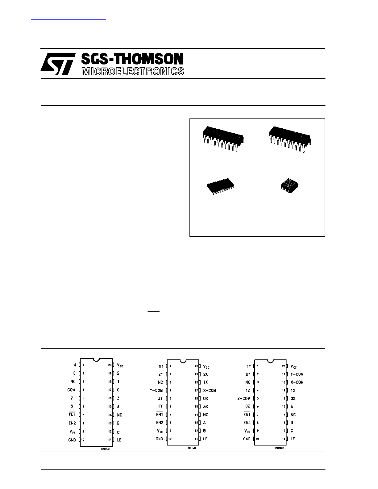
B1R
(PlasticPackage)
F1R
(CeramicPackage)
.FAST SWITCHING
.LOW CROSSTALK BETWEEN SWITCHES
.HIGH ON/OFF OUTPUTVOLTAGERATIO
.LOW SINE WAVEDISTORTION:
0.02% (TYP.) AT VCC-VEE=9V
.HIGH NOISEIMMUNITY
V
NIH=VNIL
= 28% VCC(MIN.)
.LOW POWER DISSIPATION
ICC=4µA (MAX)AT TA=25oC
M1R
(MicroPackage)
ORDER CODES :
M54HC XXXX F 1R M74H CX XXXM1R
M74HC XXXX B1R M74HCXXXXC1 R
C1R
(Chip Carrier)
DESCRIPTION
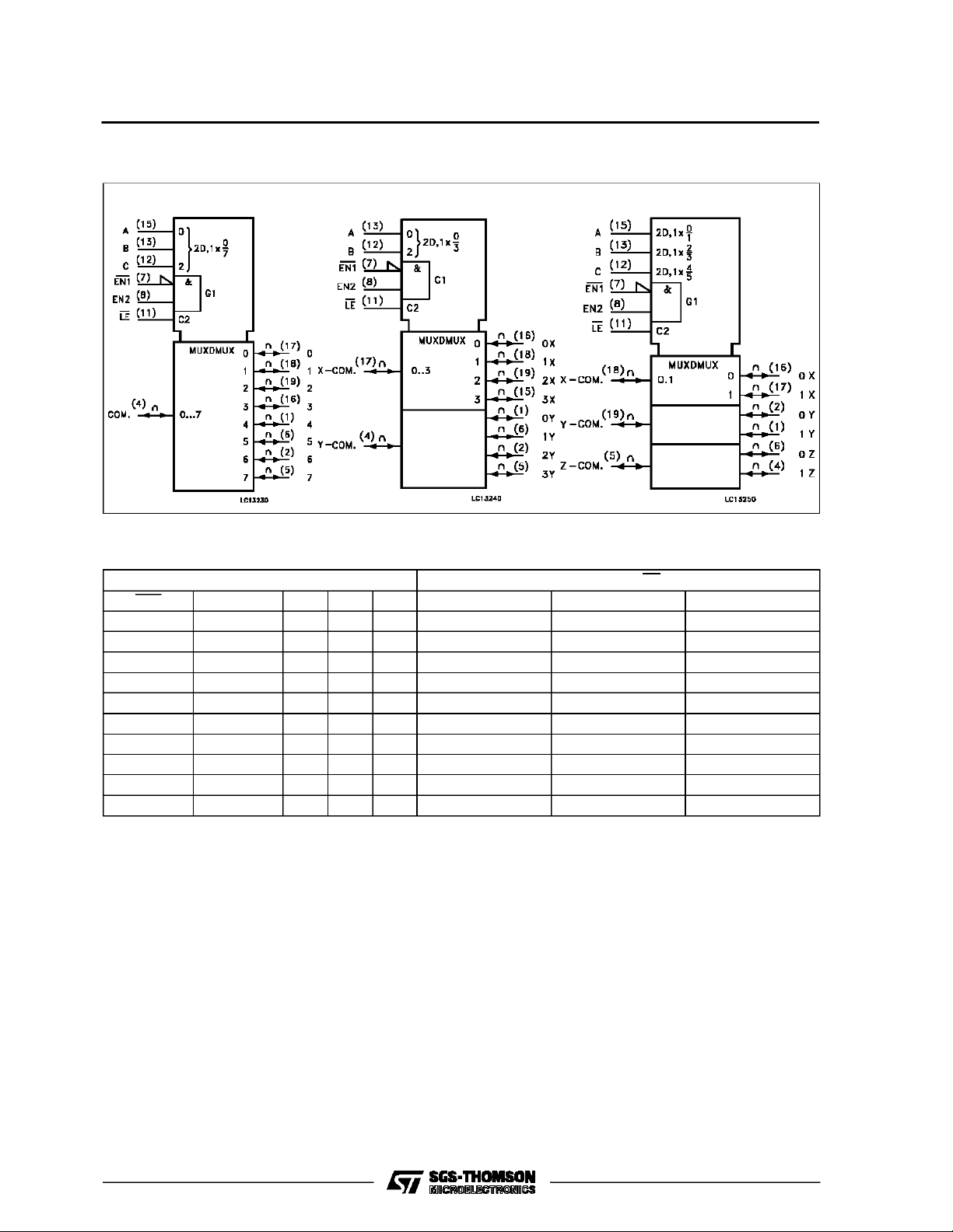
These devices are analog multiplexer
demultiplexers in high speed silicon gate C2MOS
technology. Theseanalog switchesarebidirectional
and digitally controlled. A built-in level shifting is
included to allowthema controlinput range of up to
± 6V (peak) for an analog signalwith digital control
signalof 0 to 6V.
VEEsupply pin is providedfor analoginput signals.
They have two enable inputs to enable all the
switches when high (EN2) or low (EN1). For
operation asa digitalmultiplexer/demultiplexer, V
is connected toGND.
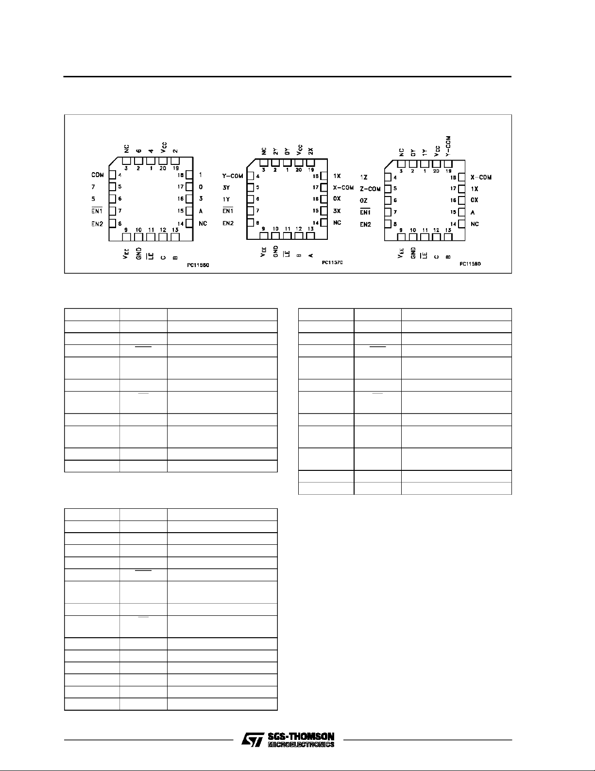
PIN CONNECTION (top view)
EE
The HC4351 is a single 8 channel multiplexer
demultiplexer havingthree binary controlinputs A,
B and C to select 1 of 8 to be turned on, and
connected to the output.
The HC4352 has a pair of four channel multiplexer
demultiplexer havingtwocontrolinputsA andBthat
selectone offour channel of the two sections.
The HC4353 is a triple two channel multiplexer
demultiplexer havingthree separate digitalcontrol
inputs A, B and C toselect independently one of a
pairof channles.
HC4353HC435 2HC4351
November1993
1/16
M54/M74HC4351/4352/4353
CHIP CARRIER
HC4353HC435 2HC4351
PIN DESCRIPTION (HC4351)
PIN No SYMBOL NAME AND FUNCTION
4 COM Common
3, 14 NC Not Connected
7 EN1 Enable Input (Active LOW)
8 EN2 Enable Input (Active
HIGH)
9V
EE
Negative Supply Voltage
11 LE Latch Enable Input
(Active LOW)
15, 13, 12 A, B, C Select Inputs
17, 18, 19,
0 to 7 Independent Input/Outputs
16, 1, 6, 2, 5
10 GND Ground (0V)
20 V
CC
Positive Supply Voltage
PIN DESCRIPTION (HC4353)
PIN No SYMBOL NAME AND FUNCTION
1, 2 0Y 1Y Independent Input/Outputs
5 Z COM Common Output/Inputs
6, 4 0Z, 1Z Independent Input/Outputs
3, 14 NC Not Connected
7 EN1 Enable Input (Active LOW)
8 EN2 Enable Input (Active
HIGH)
9V
EE
11 LE Latch Enable Input
15, 13, 12 A, B, C Select Inputs
16, 17 0X, 1X Independent Input/Outputs
18 X COM Common Output/Inputs
19 Y COM Common Output/Inputs
10 GND Ground (0V)
20 V
CC
Negative Supply Voltage
(Active LOW)
Positive Supply Voltage
PIN DESCRIPTION (HC 4352)
PIN No SYMBOL NAME AND FUNCTION
1, 6, 2, 5 0Y to 3Y Independent Input/Outputs
3, 14 NC Not Connected
7 EN1 Enable Input (Active LOW)
8 EN2 Enable Input (Active
HIGH)
9V
EE
11 LE Latch Enable Input
13, 12 A, B Select Inputs
16, 18, 19,150X to 3X IndependentInput/Outputs
17, 4 X COM
Y COM
10 GND Ground (0V)
20 V
CC
Negative Supply Voltage
(Active LOW)
Common Output/Inputs
Positive Supply Voltage
2/16
IEC LOGIC SYMBOLS
TRUTH TABLE
M54/M74HC4351/4352/4353
HC435 3HC4352HC4351
CONTROL INPUTS ”ON” CHANNEL (LE = H) **
EN1 EN2 C * B A HC4351 HC4352 HC4353
L H L L L 0 0X, 0Y 0X, 0Y, 0Z
L H L L H 1 1X, 1Y 1X, 0Y, 0Z
L H L H L 2 2X, 2Y 0X, 1Y, 0Z
L H L H H 3 3X, 3Y 1X, 1Y, 0Z
L H H L L 4 - - 0X, 0Y, 1Z
L H H L H 5 - - 1X, 0Y, 1Z
L H H H L 6 - - 0X, 1Y, 1Z
L H H H H 7 - - 1X, 1Y, 1Z
H X X X X NONE NONE NONE
X L X X X NONE NONE NONE
X: DON’T CARE *: HC4351/3only
** When latchEnable is low, the Channel Selection is latched and the Channel Address Latch does not change state.
3/16
M54/M74HC4351/4352/4353
ABSOLU TE M AXI MUM RAT ING S
Symbol Parameter Value Unit
V
CC
V
CC-VEE
V
IN
V
I/O
I
IK
I
OK
I
OUT
I
or I
CC
P
T
stg
T
AbsoluteMaximumRatingsarethosevalues beyondwhichdamagetothedevicemayoccur.Functionaloperationundertheseconditionisnotimplied.
(*)500 mW: ≅ 65oC derate to300 mW by 10mW/oC: 65oCto85oC
RECO MM ENDED OPERATIN G CO NDI TIONS
Symbol Parameter Value Unit
V
CC
V
EE
V
CC-VEE
V
IN
V
I/O
T
op
t
r,tf
Supply Voltage Range -0.5 to +7 V
Supply Voltage Range -0.5 to 13 V
DC Input Voltage -0.5 to VCC+ 0.5 V
DC Switch I/O Voltage VEE- 0.5 to VCC+ 0.5 V
Input Diode Current ± 20 mA
I/O Diode Current ± 20 mA
DC Output Current ± 25 mA
DC VCCor Ground Current ± 50 mA
GND
Power Dissipation 500 (*) mW
D
Storage Temperature -65 to +150
Lead Temperature (10 sec) 300
L
Supply Voltage 2 to 6 V
Supply Voltage -6 to 0 V
Supply Voltage 2 to 12 V
Input Voltage 0 to V
DC Switch I/O Voltage VEEto V
Operating Temperature: M54HC Series
M74HC Series
CC
CC
-55 to +125
-40 to +85
Input Rise and Fall Time VCC= 2 V 0 to 1000 ns
= 4.5 V 0 to 500
V
CC
V
= 6 V 0 to 400
CC
o
C
o
C
V
V
o
C
o
C
4/16
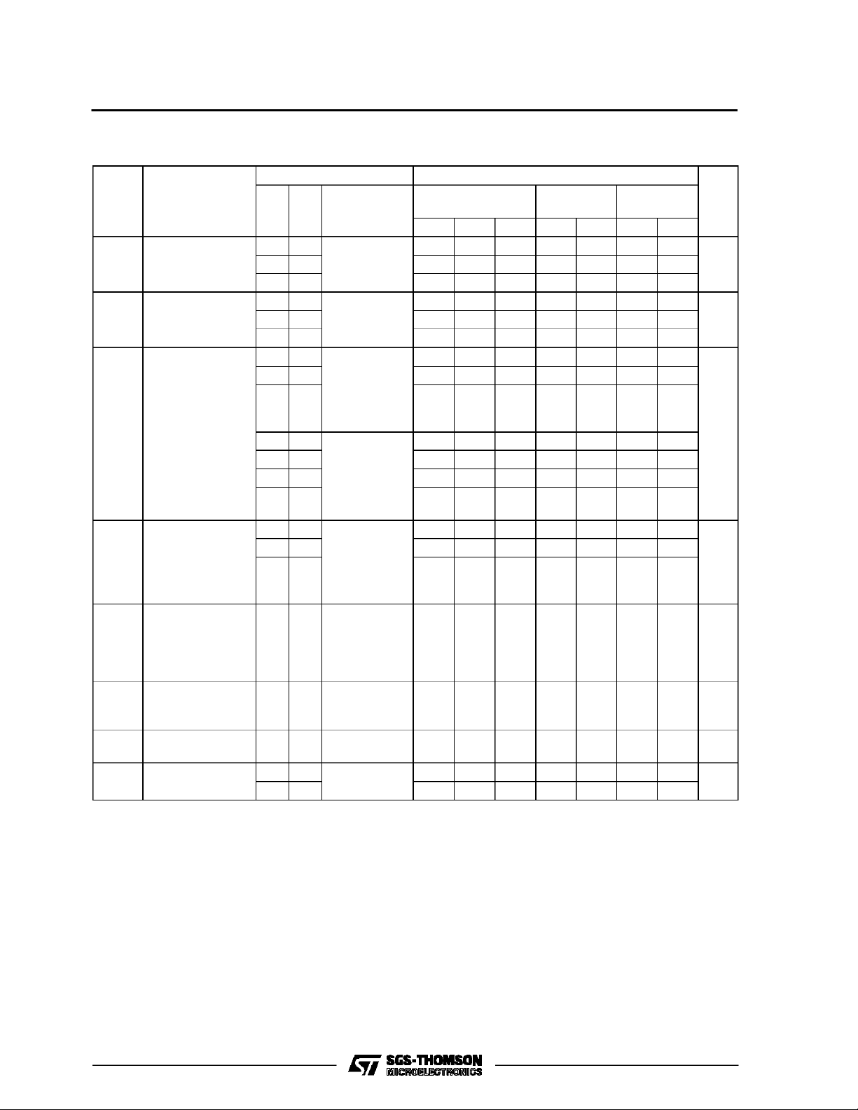
DC SPECIFICATIONS
Symbol Parameter
V
V
R
High Level
IHC
Control Input
Voltage
Low Level Control
ILC
Input
Voltage
ON Resistance 4.5 GND VIN=V
ON
M54/M74HC4351/4352/4353
Test Conditions Value
T
=25oC
V
(V)
CC
V
(V)
EE
A
54HC and 74HC
Min. Typ. Max. Min. Max. Min. Max.
2.0 1.5 1.5 1.5
4.5 3.15 3.15 3.15
6.0 4.2 4.2 4.2
2.0 0.5 0.5 0.5
4.5 1.35 1.35 1.35
6.0 1.8 1.8 1.8
or
IHC
V
4.5 -4.5 55 120 150
6.0 -6.0 50 100 125
2.0 GND V
4.5 GND 70 150 190
4.5 -4.5 50 100 125
6.0 -6.0 45 80 100
V
I/O=VCC
V
I
≤ 2mA
I/O
IN=VIHC
V
V
I/O=VCC
V
I
≤ 2mA
I/O
ILC
to
EE
or
ILC
or
EE
85 180 225
150
-40 to 85oC
74HC
-55 to 125oC
54HC
Unit
V
V
Ω
∆R
I
Difference of ON
ON
Resistance
Between Switches
Input/Output
OFF
Leakage Current
(SWITCH OFF) 6.0 -6.0
I
Switch Input
IZ
Leakage Current
(SWITCH ON)
I
Control Input
IN
Current
I
Quiescent Supply
CC
Current
4.5 GND VIN=V
4.5 -4.5 5 12 15
6.0 -6.0 5 10 12
V
I/O=VCC
I
I/O
VOS=VCCor
IHC
V
ILC
V
EE
≤ 2mA
or
10 30 35
to
±100 ±1000 ± nA
GND
VIS= GND or
V
CC
VIN=V
ILC
VOS=VCCor
6.0 -6.0
6.0 GND
GND
V
INH=VIHC
V
IN=VCC
GND
or
6.0 GND VIN=VCCor
6.0 -6.0 8 80 160
GND
±100 ±1000 ± nA
±0.1 ±1 ±1 µA
44080µA
Ω
5/16
 Loading...