

Page 1
查询M494供应商
SINGLE-CHIPVOLTAGE TUNING SYSTEM WITH
4 ANALOGCONTROLS AND µP INTERFACE
.
NON-VOLATILE MEMORY FOR 20 PROGRAMWORDS (17 BIT x 20)
- TUNINGVOLTAGE12BITS
- BAND2 BITS
- MULTI STANDARD 2 BITS
- PROGRAMSKIP BIT 1 BIT
- 10,000MODIFY CYCLESPER WORD
- MIN.10 YEARSDATARETENTION
.
13 BITVOLTAGESYNTHESIZER(BRM + PWM)
.
NV MEMORY FOR 4 ANALOG CONTROLS
(6 BITx 4)
.
4 BANDSWITCH OUTPUTS
(VHF I & III, UHF, CATV)
.
5 x 7 KEYBOARD
.
2 AUDIOVISUAL OUTPUTS (VCR& PC)
.
2 CODED MULTI STANDARD OUTPUTS
(e.g. PAL, SECAM, NTSC etc.)
.
DIRECT 11/2 DIGIT 7 SEGMENT COMMON
ANODE LED DISPLAYDRIVING
.
PCMREMOTE CONTROL RECEIVER
(M708 transmitter)
.
5-BIT DATA INPUT + CONTROL LINE FOR
P INTERFACE
.
LINEARAFC DEFEATOUTPUT
.
FLYBACK/SYNC.COINCIDENCE INPUTFOR
SEMI-AUTOMATICSEARCH
.
STANDBY OUTPUT
.
OPTIONSELECT : 16 OR 20 PROGRAMS
.
POWERUP MODE
.
PROGRAMSKIP DEFEAT
.
AVOPTIONS
.
1 * OR DECADE MODE OPTION IN 20 PROGRAM OPTION
.
TEMPORARY ANALOG UP/DOWN INDICATOR ON LED DISPLAY
.
BANDSKIP OPTION
.
455 TO 510kHz CHEAP CERAMIC RESONATOR
.
VDD=5V ±5%. VPP= 25V ± 1V
M494
pable of including a floatinggate NV memorycell
(EEPROM).
The i.c. has been designed as a complete digital
TV tuning system based on the voltage synthesis
principleand as a replacementfor all the conventional potentiometers and band switches particularly in low cost TV sets. It also provides some
functionsnormallyonlyassociatedwithhighercost
sets.NV memoryis integratedonthe chip together
withallthenecessarycontrolcircuitrytoprovidethe
program memory. Separate NV memory is also
integrated to provide the memory for four analog
controls. A seven segment LED display can be
directly driven by the chip to display the program
selected, and the direction of movement of the
analog controls. Provision is made for a remote
control receiver both on and off chip, the latter is
interfacedvia a data input and single controlline.
(Thisenablescontrol by a microprocessor).Alocal
keyboardcan be used with the device in avariety
of configurations.An optionselect pinprovides for
different program number options, power up optionsand skip associated functions. This device is
anothersignificantstep towards the completeintegration of TV control circuitry.
The device is packaged in a 40 pin DIL plastic
package.
DIP40
(Plastic Package)
DESCRIPTION
The M494 is a monolithic LSI integrated circuit
fabricatedinSGS-THOMSON’sEPM2process; an
N-channel, Planox, doublepoly MOS process ca-
June 1991
ORDER CODE : M494B1
1/22
Page 2
M494
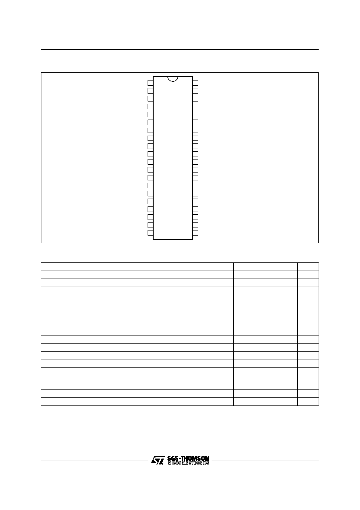
PINCONNECTIONS
OPTION SELECT
DISPLAY DRIVE
h+i
V
AV0
AV1
V
MEMORYTIMING
1
D4
2
D3
3
D2
4
D1
5
D0
6
7
8
9
g
10
f
11
e
12
SS
13
d
14
c
15
b
16
a
17
18
19
PP
20
DATA HANDSHAKE
40
V
39
DD
STANDBY
38
AFC DEFEAT
37
FB/SYNC COINCIDENCE
36
REMOTECONTROL
35
VOLUME
34
SATURATION
33
TEST 1
32
BRIGHTNESS
31
MS0
30
MS1
29
CONTRAST
28
TUNING
27
OSC. OUT
26
OSC. IN
25
VHF 1
24
VHF 3
23
CATV
22
UHF
21
ABSOLUTEMAXIMUM RATINGS
Symbol Parameter Value Unit
V
DD
V
PP
V
V
O(off)
I
OL
t
PD
P
tot
T
stg
T
op
C
os
R
os
C
dk
R
k
C
rts
Stresses above those under ”Absolute Maximum Ratings” may causes permanent damage to the device. This is a stress rating only and
functional operation of the device at theseor any other conditions above those indicated in the operational sections of this specification is not
implied. Exposure to absolute maximum rating conditions for extended periodsmay affect device reliability.
Supply Voltage – 0.3 to 7 V
Memory Supply Voltage – 0.3 to 26 V
Input Voltage – 0.3 to 15 V
I
Off State Input Voltage 15 V
Output Low Current
LED Driver Outputs : pin a-g
pin h + i
All other Outputs
20
35
5
Max. Delaybetween Memory Timing & Memory Supply Pulses 5 µs
Total Package Power Dissipation 1 W
Storage Temperature – 25 to + 125 °C
Operating Temperature 0 to + 70 °C
Capacitance on OptionSelect Pin 100 pF
Resistance on Option Select Pin 1 kΩ
Capacitance on data outputs & keyboard inputs when lines are
150 pF
connected by a keyboard switch closure
Series Resistance of Single Keyboard Switch 10 kΩ
Capacitance on Data Handshake Pin 50 pF
mA
mA
mA
494-01.EPS
494-01.TBL
2/22
Page 3
M494
STATICELECTRICAL CHARACTERISTICS (T
Pins Symbol Parameter Test Conditions Min. Typ. Max. Unit
Memory Supply I
Memory Timing V
I
O(off)
Tuning V
V
DD
I
RC V
FB/sync. Coin. Input V
V
Vol. Brigh. Sat.
Contr. DACs
V
I
O(off)
h+i V
V
V
D0, D1
D2, D3
D4
V
V
V
I
O(off)
MS0, MS1 AFC
def. AV0, AV1
V
I
O(off)
Option Select V
V
Standby V
a, b, c, d, e, f, g V
V
V
Display Drive V
I
O(off)
UHF, III, I, CATV V
V
V
V
I
O(off)
Data
Handshake
V
V
V
V
I
O(off)
Memory Supply
PP
Current
R Pull Down 25 kΩ
OL
Leakage VDD= 4.75V, VO= 26V 100 µA
OL
Supply Current VDD= 5.25V 100 mA
DD
pk to pk 0.5 13.2 V
I
IL
IH
I
IL
R Pull up 30 kΩ
OL
IL
IH
I
IL
R Pull up 200 kΩ
OH
IL
IH
I
IL
OL
R Pull up 30 KΩ
OL
IL
IH
I
IL
R Pull up 30 kΩ
OL
I
O
IL
IH
I
IL
R Pull up 200 kΩ
OL
OL
OL
OH
IL
IH
OL
OH
IL
IH
I
IL
R Pull up 30 kΩ
=0to70°C, VDD= 5V unless otherwisespecified)
amb
VPP= 25V Write Peak
Write Average
Erase Peak
Erase Average
Read Peak
Read Average
VDD= 4.75V, IOL= 2.5mA 8 V
VDD= 4.75V, IOL= 5mA 1 V
2.0 V
VDD= 5.25V, VIL= 0.8V – 0.4 mA
VDD= 4.75V, IOL= 4mA 1 V
VDD= 5.25V, VO= 13.2V 50 µA
3.5 V
VDD= 5.25V, VIL= 1.5V – 50 µA
VDD= 4.75V, IOL= 30mA 1.5 V
3.5 V
VDD= 5.25V, VIL= 1.5V – 0.4 mA
VDD= 4.75V, IOL= 1mA 0.4 V
V
= 5.5V 25 µA
O(off)
VDD= 4.75V, IOL= 1mA 0.4 V
VDD= 5.25V, VO13.2V 50 µA
3.5 V
VDD= 5.25V, VIL= 1.5V – 0.4 mA
VDD= 4.75V, IOL= 100µA 0.4 V
VDD= 4.75V, VO= 0.7V 1.6 mA
3.5 V
VDD= 5.25V, VIL= 1.5V – 50 µA
VDD= 4.75V, IOL= 15mA 1.5 V
VDD= 4.75V, IOL= 5mA 0.4 V
VDD= 5.25V, VO= 13.2V 50 µA
VDD= 4.75V, IOL= 1mA 3 V
VDD= 4.75V, IOH= – 150µA 2.4 V
3.5 V
VDD= 5.25V, VO= 13.2V 50 µA
VDD= 4.75V, IOL= 1mA 3 V
VDD= 4.75V, IOH= 150µA 2.4 V
3.5 V
VDD= 5.25V, VIL= 1.5V – 0.4 mA
VDD= 5.25V, VO= 13.2V 50 µA
35
mA
10
mA
9
mA
5
mA
8
mA
2.5
mA
0.8 V
1.5 V
1.5 V
1.5 V
1.5 V
1.5 V
1.5 V
494-02.TBL
3/22
Page 4
M494
DEFINITIONOF TERMS
The M494 has four conditions or statesthat it can
be in which are defined below. Logic LO 0V and
logic HI = 5V.
PoweredDown
V
=0V.VPP=0V
DD
On
=5V.VPP=25V.
V
DD
Devicedriving display normally.
Data Handshake pinconfigured as RTSi/p.
Standby o/p = HI. All other functions operating
normally.
Standby
=5V.VPP=0V.
V
DD
Device driving display to show a singlestatic bar
(g segment).
FUNCTIONAL DESCRIPTION (clock frequency = 500kHz)
V
DD&VSS
VDD=+5V± 5%.Whenapplied,an internalpower
onresetof110msisgenerated.Thevoltagethreshold for the reset is in the range 3 to 3.5V but is in
fact the point at which the internal clock phases
start.
V
=0V.This pin is connectedto the substrate of
SS
the i.c. and is the reference for all parameters of
the device.
Oscillator I/O
The frequencyof the oscillator should be between
445 and 510kHz using a cheap ceramicresonator.
The reference frequency of the remote control
transmitter must also be in the same range i.e. if
the oscillator frequency is 455kHz then the transmitter frequencycouldbe 510kHzor viceversa.
Test
Thispinis normallyusedforpost fabricationtesting
purposesonly andshould betied to V
. However
SS
this pin can be used by SGS-THOMSON or the
OEM to enable external loading of the memory.
Details of how to achieve this can be furnishedby
SGS-THOMSON.
DataHandshakepinconfiguredasRTS i/p.Stanby
o/p =LO.
All keyboard commands are disabled except any
programcommand On/Off, On/Stanby.
Memory sequence up or down, 1 * and ±10 (decade) commands.
Analog controls. Tuning, AV, MS and AFC defeat
o/p’s = LO. Band o/p’s= HI (externallypulled up).
See Standby section for more detail.
Off
V
DD
Data Handshakepin configuredas OFF o/p.
Standby o/p = LO. Display disabled and Display
driveo/p = HI (externallypulled up).
All keyboard commandsdisabled except ON/OFF.
Remoteand data command sources disabled.
Analog controls, Tuning, AV, MS and AFC defeat
o/p’s = HI (externallypulled up).
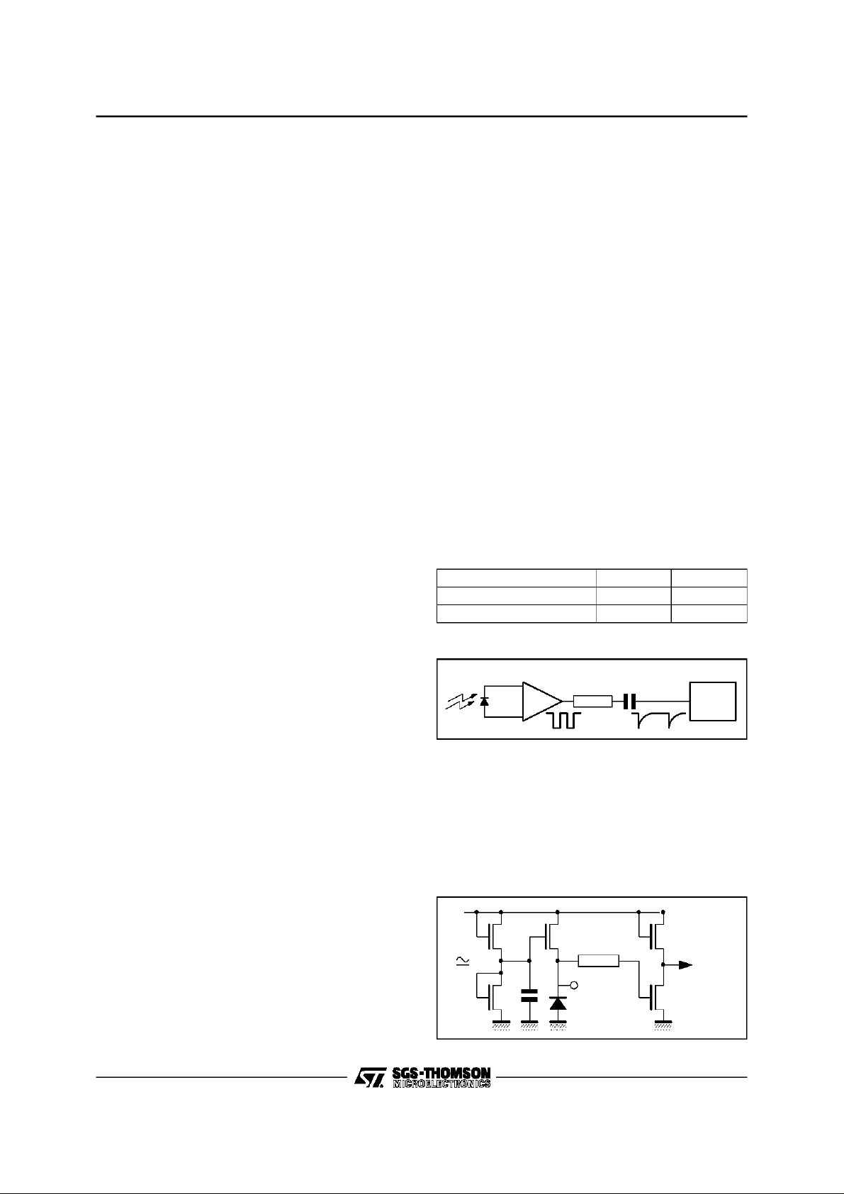
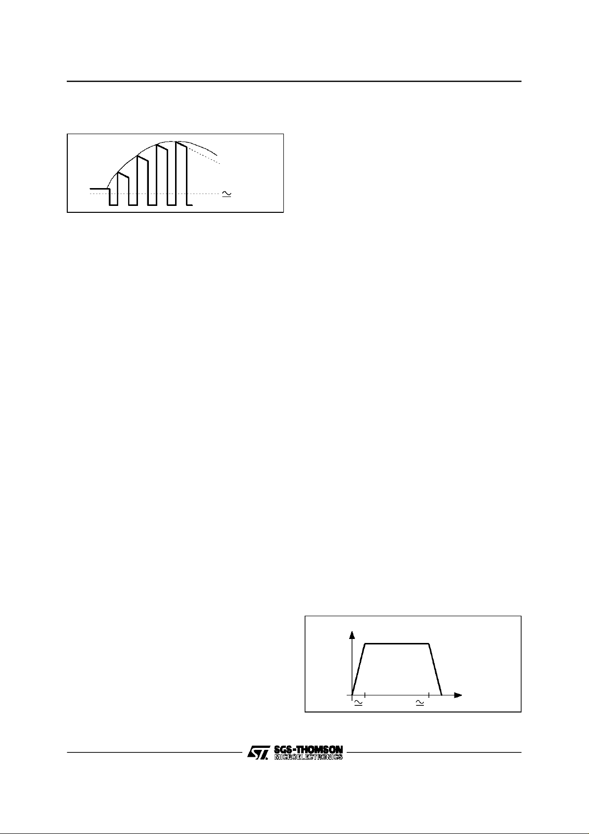
The signal from the preamplifier (TDA8160) is
broughtto the RC signal input via an AC coupling
network(seeFigure 1).
Figure1
The input is self biased to approx. 1.5V. When a
largesignal is applied to the input a levelshift will
take place predominantlydue to the coupling network.
Howeveranother time constantis alsovisible due
to the coupling C and the internal resistorR
Figures. 2 & 3).
Figure2
=5V.VPP= 0V. Device not driving display.
VDD(TDA8160) R C
5V 2.2kΩ 4.7nF
12V 10kΩ 4.7nF
TDA8160
RC
M494
. (see
i
V
DD
494-02.EPS
Remote ControlInput
The integratedRCreceiver decodessignalstransmitted by the M708 (address 10). The minimum
signal amplitude should be 0.5V peak to peak at
the input pin. The minimum pulse width should be
8µs.
4/22
1.5V
Ri
to Cct
Remote
ControlI/P
494-03.EPS
Page 5
FUNCTIONAL DESCRIPTION (continued)
Figure 3
τ
=RC
1
τ
=Ri.C
2
1.5V
Severaltests are performedon the signal :
a) Measurement of the pulse distance T (time
base synchronization).
b) Check of the bit positions relative to the time
basewindows.
c) Checkof theparity bit.
d) Check oftheabsenceof pulsesbetweenparity
and stop pulses.
e) Check of the noise level. The receiver checks
the noise level for a time T after each pulse
detected.
If all these tests are successful the received word
is stored and decoded. If not it is rejected. The
transmissionis terminatedon receptionof the end
of transmission (EOT) code or if the internal timer
measuresatransmission interruptionof morethan
550ms. For more detail concerning the operation
of theRC receiver refer toSGS-THOMSON Technical Note No. 155 pp11-12.
The RC receiverand the local keyboardhave the
same command source priority i.e. a local command is not accepted until a previously accepted
RC commandhas been completelyexecuted and
the EOTcode transmitted. Similarly if alocalcommand isunder executionthenan RCcommandwill
not be accepted. The RC truth table and commandsare shownon the next page.
Analog Control Outputs
Four analog control outputs are implemented to
provide for Volume, Brightness, Saturation and
Contrast from four 6 bit D/A’s. TheseD/A’suse the
Pulse Width Modulation technique to synthesize a
pulse trainof constantfrequencybut variablepulse
width (PWM). Each output delivers a 7.8kHz
square wave whose duty cycle is variable in 63
steps. External RC filtering and level shifting is
required to realise a static DC voltage from the
pulse train. If the analog outputs are continuously
varied by command from the keyboard or data
commandsourcesthe outputswill change approx.
every 112ms (fck = 500kHz) or approx. every
102ms if the command is issued from the RC
command source. One analog control is specifi-
callydesignedasa volumecontrolas mutecircuitry
isbuilt in.
On start up resetthe analogcontrol outputs except
volume are enabled after a period of approx.
1.1 seconds. In the Standbyand Off statesall the
analogcontrol outputs arepulled to logicLO.
The normalise command reads the contents of
each analog memory sequentially to its corre-
494-04.EPS
spondingcounter and D/Aoutput.
Tuning Output
The tuning voltage is generated from a 13 bit
counter.Theprogrammemorystoresthe 12MSB’s
of the tuning word. The range of the AFC circuitry
is at least 3 bits so the LSB of the tuning counter
doesnot affectthe resolutionof tuning.
Thecontents of the counterare convertedusing a
PWM and a Bit Rate Multiplier (BRM) technique.
13 bits gives 8192 steps which yields a resolution
ofapproximately3.9mVwith a max. tuning voltage
of 32V. This corresponds to a resolution of about
75kHzin the UHF band. The 5 MSB’sof thetuning
word areconverted using PWM and the remaining
8 bits using BRM. Thus as the tuning word increasesfromall zeroesthenumberof pulsesinone
period increases to 256 with all the pulses being
the same length (t
=2µs). Forvalues larger then
o
256 PWM conversiontakes placewhere the number of pulses in one period stays constant at 256
but the width changes.
Whenthepulsewidth reaches15t
twosuccessive
o
pulses ”link” together and the number of pulses
decreases(see Figure 4).
Thepulse trainis fed toan externallow pass filter
to realise a DC voltage. The temperaturedependence of thissystem is predominantlythe switching
times of the output pulses and asthere are only a
maximumof256 pulsesin oneperiodthetemperaturestability is very good.
InStandbyand Offstatesthetuningoutputispulled
to logic LO.
Figure4
No OF PULSES
256
TUNING
1V 31V
VOLTAGE
M494
494-05.EPS
5/22
Page 6
M494
FUNCTIONAL DESCRIPTION (continued)
Table1 : RemoteControl Commands(address 10, code =1010)
Command
Number
0
1
2
3
4
5
6
7
8
9
10
11
12
13
14
15
16
17
18
19
20
21
22
23
24
25
26
27
29
28
30
The above table showns the differencebetween the 16 and 20 program optionswith respect to the remote control commands. Commands 16,
17, 18 &21 change function between the two options. Commands 22, 23 & 24 should not be used in the 20 program option, as theyhave no
function.
NOP = No operation
16 Programs 20 Programs C1 C2 C3 C4 C5 C6
EOT
Standby
Mute (toggle)
Program 1
Program 2
Program 3
Program 4
Contrast up
Contrast down
Program 5
Program 6
Program 7
Program 8
Memory Seq. up
Memory Seq. down
Program 9
Program 10
Program 11
Program 12
Normalise
On/stby (tog.)
Program 13
Program 14
Program 15
Program 16
Volume up
Volume down
Brightness up
Brightness down
Saturation up
Saturation down
Function Code
EOT
Standby
Mute (toggle)
Program 1
Program 2
Program 3
Program 4
Contrast up
Contrast down
Program 5
Program 6
Program 7
Program 8
Memory Seq. up
Memory Seq. down
Program 9
Program 0
– 10 (decade)
+ 10 (decade)
Normalise
On/stby (tog.)
1*
NOP
NOP
NOP
Volume up
Volume down
Brightness up
Brightness down
Saturation up
Saturation down
0
1
1
0
1
0
1
1
1
0
1
0
1
1
1
0
1
0
1
1
1
0
1
0
1
1
1
0
0
1
1
0
0
1
0
0
1
1
0
1
0
0
1
1
0
1
0
0
1
1
0
1
0
0
1
1
0
1
0
1
0
1
0
0
0
1
1
1
1
0
0
1
1
1
1
0
0
1
1
1
1
0
0
1
1
1
1
0
0
1
1
1
1
0
0
0
0
0
0
0
0
0
0
0
0
0
0
0
0
0
0
0
0
0
0
0
0
0
1
1
1
1
1
1
0
0
0
0
0
0
0
1
1
1
1
1
1
0
0
0
0
0
0
1
1
1
1
1
1
1
1
1
1
1
1
0
0
0
0
0
0
0
0
0
0
0
0
0
1
1
1
1
1
1
1
1
1
1
1
1
1
1
1
1
1
1
Program Memory
NV memory(EEPROM)is integratedon thechipto
provide storage for up to20 stations.
Each memorylocationis 17 bits inlengthproviding
12 bits fortuning voltage,2 bits for band, 2 bits for
two coded multi-standard outputs and 1 bit program skipflag.
Individualprogramwordscanbe readoncommand
from the keyboard, remote or data command
sources but can only be written oncommandfrom
the keyboard.
There are twomethods for storing a program(writing the memory): pre and post tuning selectionof
the programnumber. See Commands, section7.
Readingeach memory locationin sequence(up or
down) can also beachievedfromall thecommand
sources.
All memory timing functionsare provided on chip
and only one external transistor is required to
switch the external memory supply (25V).
6/22
Thereare essentiallytwo operationscarriedouton
the memory: Write/Modifyand Read.
The Write/Modifycycle consistsof 3 steps :
a) All ”1s” are written to thebits of theaddressed
word.
b) All bits of the word are erased.
c) The new contents are written.
Usingthismethodallthebitsof theaddressedword
are aged thesame.Formore detail concerningthe
write, erase and read current waveforms at the
Memory Supplypin seeM491 datasheet.
MemoryFor Analog Controls
The memory for the analog controls is electrically
identicaltothemain programmemory butis organised as four 6-bit words located in two sequentially
addressed words at the memory. Each word corresponds to the Volume, Brightness, Saturation
and Contrast outputs. At power on reset and normalise commandeachmemory word is readout to
its corresponding counterand D/Ain sequence.
Page 7
FUNCTIONAL DESCRIPTION (continued)
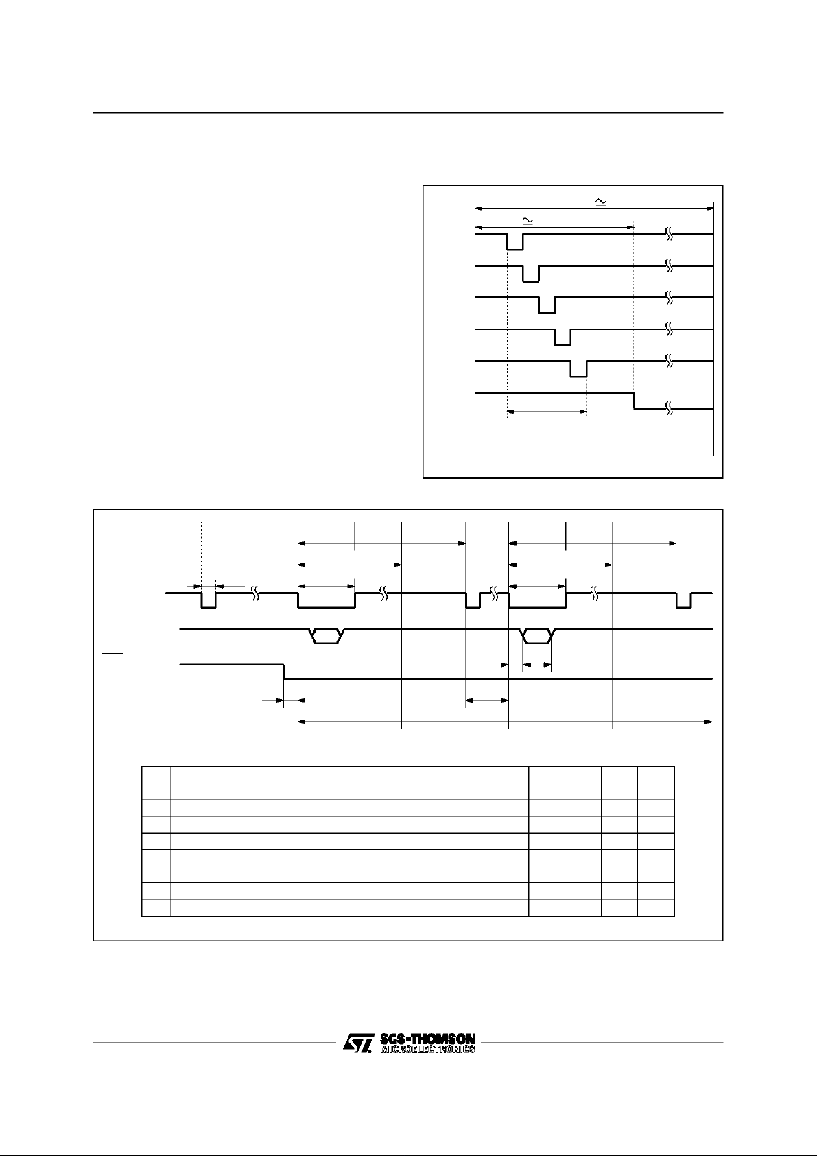
Display,Keyboard and Data Multiplexing
Logic is integrated on the chip to provide the multiplexing between the display, keyboard and data
inputs. In the On state and with the Data Handshake pin at logic HI as an input the display and
keyboardare muxed together.See Figure 5. Each
column output goes to logicLO in sequence and
the row inputs are scanned for a key closure. In
chronological order across the total mux. period
there is : initialisation, scan, decision and display
periods.
The Data Handshake pin has a complex logical
function. It hastwo modesof operation: as a hand
shake I/O line to a µP and as an output line to the
P to signalthat theM494is in theOff state.In order
to achieve this function careful signal timing is
required both internally and externallyto the chip.
See Figure6. Whenthe deviceis in the OFFstate
the Data Handshake pin is used to signal this
condition to theµP by being pulled LO.
Figure 6 : Data-input-timing
Figure5
D0
D1
D2
D3
D4
DISPLAY
DRIVE
( 2ms)
INITIALIZE
MUX PERIOD (8ms)
640µs
SCAN
DECISION
M494
DISPLAY
494-06.EPS
A1 B1 C1 D1 A2 B2 C2 D2 A3
DATA
HANDSHAKE
D0 - D4
EOE
(END OF TRANSMISSION)
DATA HANDSHAKE
NOT TO SCALE
PIN CONFIGURATION
N° Symbol Parameter Min. Typ. Max. Unit
1t
RTS
2t
CTS
3t
O/P
4t
HS
5t
6t
7t
8t
Note : Oscillator Clock = 500kHz
S
H
J
CR
t
CR
t
O/P
t
RTS
t
j
t
CTS
DATA DATA
t
t
HS
t
t
S
CTS
H
t
CR
t
O/P
K/B AND RC I/P
DISABLEDTILL
EOT EXECYTION
(EOT = END OF
O/II/OO/II/O
TRANSMISSION)
Request to Send Pulse (RTS) 5 10 µs
Clear to Send (CTS) 512 µs
Pin Output Configuration 8 ms
Handshake Time 12 µs
Data Set up Time 10 128 µs
Data Hold Time 128 256 µs
Synchronization Jitter 8 ms
CTS tonext RTS Pulse 98 ms
494-07.EPS - 494-03.TBL
7/22
Page 8

M494
FUNCTIONAL DESCRIPTION (continued)
Display
The M494 is capable of directly driving a 1 digit
common anode LED displayat the max. sink current of 15mA per segment.The h+ipin is capable
of sinkinga max. currentof30mAso that thesetwo
segments can be drivenfrom the same pin and be
the samebrightness as the other segments.
On instructionfrom theinternal command decoder
the displayshows programmenumber,directionof
analogcontrolmovement,decadechangeor Memory Addressingfunction active. Analog controls in
this context are defined as Tuning, Volume,Contrast, Saturation & Brightness. The formats of the
displayforanalogcontroldirection,decadechange
and Memory Addressingare shown belowrespectively :
UP DOWN MEMORY
ADDRESSING
For the analog controls the above condition is
displayedwith an”overrun” time of 300ms.i.e.the
display will show the ”arrows” for a period of
300ms after the release of any analog control up
or down key. The Memory Addressing function
displayflashesat5HzaftertheMemoryAddressing
functionis commandedand continuesto flash until
a programmeis selectedor anyother command is
given. In1 * the g segmentonly flashesat 5Hzand
continues to flash until a programme number is
selected or any other command is given. If in
Memory Addressing and 1 * is pressed then the
display above is shown with segments g &d only
flashing at 5Hz until a programme number is selected or any other commands is given. When
Store orSet SkipFlag commandsareexecutedthe
whole display is flashedat 5Hz for 1second.
Keyboard
It is possibleto implement a keyboard with a max.
size of 35 keys as a 5 x 7 array.Fig. 8 shows the
arrangement ofthe key matrix. Each key connects
a row (a-g) with a column (D0-D4) with a max.
resistance of 10kΩ. De-bouncelogic is integrated
on the chip that only allows acceptance of a command if the key is closed for longer than 40ms
except for the On/Standbyand On/Off commands
wheretherelevantkeysmust beclosedforapproximately 100ms. Thisis equivalentto 2 receivedRC
commands).
|* I* AND
MEM.ADDR.
For the main keyboardmatrix (a-g x D0-D4), if the
logic detects two keys closed simultaneously the
display is blanked to indicate this condition to the
userand no commandis executed.When thelogic
detectsonly one key pressed the displaywill re-illuminateand the command be executed.
Thisavoidsconfusionasto whichcommandshould
be executed and provides feed back to the user.
For the Option select line all options/commands
canbe active simultaneously.
1 * mode or decade mode can be selected on the
optionselect line by the presenceofa diode ornot
respectively.These two modes are only active for
the 20 programoptionand are describedbelow :
In 1 * mode the display will toggle in & out of the
conditionshown in the Display Section. Access to
programs in the first decade is made by simply
pressing any 0-9 program key and access to programs inthe seconddecade, whateverthe current
program is made by pressing 1 * followed by any
0-9 program key.
494-08.EPS
In decade mode on pressingeither ±10 (decade)
keysthe displaywill light or extinguishthe halfdigit
respectively and simultaneously effect the tuning
information.e.g. ifthe deviceisin program 3pressing+10 (decade)key willgiveprogram13andthen
pressing - 10 (decade) key will give program 3.
Pressing- 10 (decade)again will have no effect.
The 20 program option select acts like an enable
for the 1* or decademodes. i.e. the 1 * or decade
modes are only selectablein the 20 program option. In 16 program option the function of the 1*
key,programkey 0, -10(decade) & + 10 (decade)
are changed to no function, programme 10, 11&
12 respectively. i.e. The differencebetween fig. 7
& 8 for those keys thatchange function.
If the 1 * key ispressed followedby brightness up
for examplethe device willincrease the brightness
only and reset the 1 * command i.e. the last
command from any command source will always be executed if it is a single keystroke
commandand the 1 * command willbe reset by
it. Itis possibleto pressthe 1* keyon thekeyboard
andthen aprogram0-9commandfromRC orData
commandsourcesor vice versa.Thus there are2
methodsof selectinga program fromthe keyboard
for the 16 program option : directaccess (only up
to 12 programs) or Memory sequence up/down.
And there are 3 methods of selecting a program
from the keyboardfor the 20 programoption : 1 *
mode, decade mode and Memory sequence
up/down.
8/22
Page 9

FUNCTIONAL DESCRIPTION (continued)
Figure7 : Keyboard16 Programs
M494
1
2
3
4
5
6
8
9
10
11
12
NORMALIZE CONTRASTUPSTORE
PROGRAM
ON/STANDBY
(TOGGLE)
VOLUME
UP
VOLUME
DOWN
SET SKIP
FLAG
SATURATIONUPMEMORY
CONTRAST
DOWN
BRIGHTNESSUPTUNE
BRIGHTNESS
DOWN
ON/OFF
(TOGGLE)
SEQUENCE
UP
STORE
ANALOG
VALUES
UP
TUNE
DOWN
BAND
SEQUENCE
MS
SEQUENCE
a
b
c
d
e
M494
7
MUTE
(TOGGLE)
SATURATION
DOWN
MEMORY
SEQUENCE
DOWN
MEMORY
ADDRESSING
f
16* AV1*
AV2
* = DEFAULT P/U =POWER UP
P/U*
OFF
P/U
STANDBY
g
OPTION
SELECT
SKIP OFF
h+i
D0
D1
D2
D3
D4
494-09.EPS
9/22
Page 10

M494
FUNCTIONAL DESCRIPTION (continued)
Figure8 : Keyboard20 Programs
1
2
3
4
5
6
8
9
0
-10
DECADE
+10
DECADE
1*
NORMALIZE CONTRASTUPSTORE
PROGRAM
ON/STANDBY
(TOGGLE)
VOLUME
UP
VOLUME
DOWN
SET SKIP
FLAG
SATURATIONUPMEMORY
CONTRAST
DOWN
BRIGHTNESSUPTUNE
BRIGHTNESS
DOWN
ON/OFF
(TOGGLE)
SEQUENCE
UP
STORE
ANALOG
VALUES
UP
TUNE
DOWN
BAND
SEQUENCE
MS
SEQUENCE
a
b
c
d
e
M494
7
MUTE
(TOGGLE)
SATURATION
DOWN
MEMORY
SEQUENCE
DOWN
MEMORY
ADDRESSING
f
10/22
AV1*
20
* = DEFAULT P/U = POWER UP
AV2
P/U*
OFF
P/U
STANDBY
DECADE*
MODE
1*MODE
g
OPTION
SELECT
SKIP OFF
h+i
D0
D1
D2
D3
D4
494-10.EPS
Page 11

M494
FUNCTIONAL DESCRIPTION (continued)
Data Input
Shown below are the codes for the commands :
see Table2.
The Data input will acceptsignals whosetiming is
defined in Figure 6 and electrical characteristics
defined in the table of static electrical characteristics. The EOT code must be transmittedafter
each command after amin. periodof 112ms.
Band Outputs
Four band outputsare providedfor selection ofthe
signalband:VHF I &III, UHF andCATV.Bandskip
logic is implemented so that by tieing the relevant
pin to V
a band can be skippedin regions of no
SS
transmission in that band. The bands can be se-
Table2 : DataCommands
Command
Number
0
1
2
3
4
5
6
7
8
9
10
11
12
13
14
15
16
17
18
19
20
21
22
23
24
25
26
27
28
29
30
The above table shown the differencebetween the 16 and 20program options with respect to the Data input commands.
Commands 10, 11, 12 & 13 change function between the two options. Commands 14, 15 & 16 should not be used in the 20 program option,
as they have no function.
NOP = No operation.
16 Programs 20 Programs D0 D1 D2 D3 D4
EOT
Program 1
Program 2
Program 3
Program 4
Program 5
Program 6
Program 7
Program 8
Program 9
Program 10
Program 11
Program 12
Program 13
Program 14
Program 15
Program 16
Normalise
Volumeup
Volumedown
Contrastup
Contrastdown
Brightness up
Brightness down
Saturation up
Saturation down
Memory Seq. up.
Memory Seq. down
On/standby (toggle)
Standby
Mute (toggle)
NO TRANSMISSION (pulled up) 1 1 1 1
Function Code
EOT
Program 1
Program 2
Program 3
Program 4
Program 5
Program 6
Program 7
Program 8
Program 9
Program 0
– 10 (decade)
+ 10(decade)
1*
NOP
NOP
NOP
Normalise
Volume up
Volume down
Contrast up
Contrast down
Brightness up
Brightness down
Saturation up
Saturation down
Memory Seq. up.
Memory Seq. down
On/standby (toggle)
Standby
Mute (toggle)
lected only in a rolling sequence by the band sequence keyboard command. The sequence is as
follows : VHF III, UHF, VHF I, CATV.
Multi Standard Outputs
Twocoded multi standard outputs(or generalpurpose TV system flags) are provided so that theTV
set can be designed for use in areasof more than
one transmission standard. This function requires
an externaldecodertorealise4differentstandards
e.g. PAL1, PAL2, NTSC, SECAM etc. The multi
standard sequence command available from the
keyboard gives a simple binary count at the two
outputs : 00, 01, 10, 11,00 etc. In Standbyand Off
statesthe multistandard outputs are pulled to logic
LO.
0
1
1
1
0
1
0
1
0
1
0
1
0
1
0
1
0
1
0
1
0
1
0
1
0
1
0
1
0
1
0
0
0
0
1
0
0
1
1
0
0
1
1
0
0
1
1
0
0
1
1
0
0
1
1
0
0
1
1
0
0
1
0
0
0
0
1
1
1
1
0
0
0
0
1
1
1
1
0
0
0
0
1
1
1
1
0
0
0
0
1
1
1
0
0
0
0
0
0
0
0
1
1
1
1
1
1
1
1
0
0
0
0
0
0
0
0
1
1
1
1
1
1
1
0
0
0
0
0
0
0
0
0
0
0
0
0
0
0
0
1
1
1
1
1
1
1
1
1
0
1
1
1
1
1
11/22
Page 12

M494
FUNCTIONAL DESCRIPTION (continued)
AudioVisual Outputs
Twoaudio visualoutputsareprovidedfor automatic selection of a VCR and/or personal computer.
ThelogicstateofthepinsdependsontheAVoption
selected, the program option and the program
number selectedaccording to the truth tables below :
Table3 : AVOption 1 (16/20 Programs)
Program AV0 AV1
16/0
15/19
Others
Table4 : AVOption 2 (16/20 Programs)
Program AV0 AV1
8/8
7/7
6/6
Others
External pullup resistors must be used to realisea
logic HI asthe outputs are opendrain transistors.
See I/OConfiguration.
AFC Defeat Output
The AFCdefeat output is a TTL compatiblesignal
that is capableofswitchingthe AFC circuitry inand
out. The AFC defeat output is pulled LO on any
program change including memory sequence up
and downand is heldLO for 500msafterexecution
of thecommand.When tune up or downare commandedtheAFC defeatoutputistakento logicLO.
After the tuning operation the AFC defeat is held
LO for 1 second after the key is released (see
Figure 9). Onpower on& start up resets it is taken
to logic LO for approx. 1.1seconds.
Figure9
TUNE UP/DOWN:
KEYED
AFC DEFEAT
OUTPUT
RELEASED
Standby
The standby output is a push pull output capable
of directly drivingan NPN transistor for switching
a relay. The states of this pin are defined in the
definition of terms. When standbyis commanded,
availablefrom all commandsourcesas Standbyor
On/Standbycommands, the standby output is enabled.
1
0
0
1
0
1
0
1s
0
1
0
0
1
1
0
If the device goes into Standby from On then any
program command will bring the device On with
that programselected.On/Offcommandfrom keyboard only will execute the Off function.
On/Standby, Memory sequence up or down, 1 *
and ± 10(decade)commands from any command
source will bring the device On in the program
selected before Standbywith the displayshowing
that program only,i.e. the device executes an On
commandonly.
IfthedevicegoesintoStandbyfromPowereddown
thenthe On/Offcommand fromkeyboardonly and
any program command, On/Standby,Memory sequence up or down, 1 * and ± 10 (decade)commands from any command source will bring the
device On in program 1. i.e. the device executes
an On command only.
Option Select
The Option select pin provides an extra line that
performs a ”hard wired keyboard function” in conjunction with the keyboard scanning lines D0-D4.
This line has integrated logic associated with it
that enables one or many of the functions to be
active simultaneously. In contrast, the keyboard
inputs a-g will allow one key active at any given
time. See keyboard section.
Various options can be selectedby theconnection
or not of a diode as shown in Figures7 & 8.
From left to right along the Option select line column 1 selects the number of programs. A diode
connectedhere selects 20 programs (full complement)and no diode (default) selects16 programs
onlythat canbe accessed.The 20 program option
only enables selection of 1 * or decade modes in
column 4. In column 2 the AV option defines the
stateof the AV outputs for twoprotocols.
Thesearedescribedin sectionAudiovisualoutput.
Column3definesthestate the M494powers up in.
If no connectionof a diode (default) is made here
the device powers up in the Off state. If a diode is
494-11.EPS
present then the device powersup in the Standby
state. In column 4, activated by the 20 program
option only, the presence of a diode places the
device in 1 * mode and the absence of a diode
selects decade mode. The diode and switch in
column 5 defeats the skip condition and enables
program memory words to be read with the skip
flagset.
This allows programming (or reprogramming) of
previouslyskipped words.
12/22
Page 13

FUNCTIONAL DESCRIPTION (continued)
Skip Function
Program skip is implemented in the M494 by a
single memory bit associated with each program
word.The bit acts asa flagto thedeviceto indicate
that the programword should be skippedand the
next program word read from the memory in ascending or descendingorder if the skip flag is set.
Programs are skipped only when accessed using
the memorysequenceup/downcommands.Direct
accesstoa programfrom thekeyboard,RC ordata
command sources will always override the skip
function. e.g. if skipis set on prog. 7 and prog.7 is
commanded from RC then prog. 7 will be tuned
even if there is nc prog. stored in that memory
location.
In order to program the skip bit and to defeat its
function when required two commands are available : setskipflag andskip defeat.Theskip defeat
switch is designed to be activated by a faciapanel
on the TV set under which are infrequentlyused
controls.
On the set skipflag commandthe M494 stores the
currentcontentsof thetuning, band andMS counters and sets the skip bit. After the set skip flag
operation the contentsof thetuning,band and MS
counters will not change and the device continues
to output these values. The operationis transparent to the user in termsof functionbut is indicated
on the display by the program number flashingat
5Hz for 1 second. In order to reset the skip bit for
any program word thedesired program shouldbe
selected with skip defeated. Astation shouldthen
be tuned,if required,andthen the store command
issued. The store command automatically resets
the skip flag.
The skipdefeatcommandenablesthe readingand
writing(plusresettingof skipflag)of memorywords
whoseskipflag is set.If skipisdefeatedthe device
will only access the number of programsselected
by the option select i.e. If 16 programs only are
selected then skip defeat will NOT enable access
to all20 programs.
Reset
There are twoconditionsunder which the M494 is
reset : power on and start up (On command).
Power on reset is triggered whenever V
DD
falls
below about 3V.
The duration of this reset is 110msafter V
DD
has
been restored.
M494
Power On Reset
(Powereddown to Offor Standbystates)
After the reset periodof 110ms:
a) The program counter is set to program1.
b) The outputs are disabled as defined in the Off
and Sta nd by sta tes. See Standby & Off
definitions.
c) The option selection, keyboard, momentary on
switchand,wheninstandby,thedisplay, RCand
data inputs become active. For the ”activity
level” ofthe keyboard inOff andstandbystates.
SeeStandby & Off definitions.
d) An internal register is set to indicate that the
devicehas powered up from the powereddown
state.
Start Up Reset
(Standbyor Off states to On state)
Astart upresetis instigated by thereceptionof the
commands given in the definition of terms or the
Standbysection.
The followingthen occurs :
a) The internal register indicating that the device
has powered up from the powered down state
isread :
I) If the register is set than the memory word
addressedby the program counter is loaded
into the tuning counter and then the analog
valuesare read rom thememory.
II) If the register is reset then the previously
selected tuning and analog values are left
unchanged.
b) The AFC is defeatedand the volumemuted for
a period of approx 1.7 secondsor 0.6seconds
longerthan the other analogoutputs.
c) The tuning and analogue outputs, except
volume,are enabledafter approx. 1.1 seconds.
d) The volumeoutput is enabled after 1.7 seconds
e) The standby output is pulled up internally to
logicHI
f) The internal register is reset.
If the device has either of the power up options
(power up in Off or standby states)selected then it
willperformapowerup resetbutall theoutputsand
commandsourceswillremaindisabled,thenonthe
On command,a start up reset will be performed.If
the device is required to power up in the On state
using the momentary mechanical switch connectedto the h+ipin thenit will performanordinary
power on resetfollowed immediatelyby a startup
reset. The outputs and command sources will be
enabledafter the periods defined above.
13/22
Page 14

M494
FUNCTIONAL DESCRIPTION (continued)
Manual Tuning
Manual tuning commands tune up or down, are
available from keyboard only and are provided to
allow both manual station search and tuning
adjustments. If a continuous tuning up or down
commandismade from the keyboardthe speedof
movement of the tuning counter is as shown in
fig. 10 for the UHFand CATVbands. Timet
isthe
o
start time for the key being pressed. When the
FB/sync. coincidenceinput is a logic HI thetuning
speed is reduced to 16 steps/sec. If, at time t
the
o
FB/sync.coincidence input is at logic LO than the
tuning.sweep speed jumps immediately to 512
steps/sec.
For VHF III & I all these levels are shiftedup bya
factor of 2 & 4 respectivelygiving slowest speeds
of 8 steps/sec. and 16 steps/sec. and highest
speeds of 1024 steps/sec and 2048 steps/sec. If
the continuity of command is broken by releasing
the keyboard for example then the tuning speed
returns to its slowest speed when the FB/sync.
coincidenceinputis atlogic HI.Ifthe upperorlower
limitofa bandisreachedduring manualtuningthen
tuning will continuein the same directionfrom the
Figure10 : TuningSweep Speed (UHF & CATVBANDS)
opposite limit after a 480msdelay to allow for the
dischargeof the external network.
The tuning counter is 13 bits in length giving a
range of 8192 steps. The UHF band has a bandwidth of approx. 400MHz. Thus in the UHF band
the slowest speed of 4 steps/sec. gives a tuning
speed of about 200kHz/sec. The fastest speed of
512 step/sec. corresponds to a total band sweep
time of 16 seconds.
Program Memory Sequence
Acontinuousup/downprogrammemorycommand
from keyboardproduces a program change every
500ms. From remote control and data command
sourcesa continuousprogram memorysequence
command produces a program change approx.
every 500ms or every 5 received commands. A
memory sequence up or down command issued
fromanysourcewillbringthe deviceout ofstandby
to the program selected before standby was commanded. The memory sequence up or down will
not thencommenceuntil the command isstopped
and reissued from any source (until an EOT has
been received or internally generated).
TUNING SWEEP
SPEED (STEP/SEC)
512
32
16
8
4
t0123
FB/SYNC.
COINCIDENCE
FB/SYNC.
COINCIDENCE
Time (sec)
FB/SYNC.
COINCIDENCE
494-12.EPS
14/22
Page 15

FUNCTIONAL DESCRIPTION (continued)
Mute
The sound mute function is available as a toggle
command fromall commandsources.
There are other commands and functions during
which the soundis muted :
- FB/sync. coincidence - If there is no FB/sync.
coincidence under any conditions the sound is
muted.
- Startup reset- the soundismuted forapprox.1.7
seconds.
- Program change - the sound is muted for 0.6
seconds on any program change ; direct, 1 * +
0-9 program (only after the second keystroke),
±10 (decade)& Memory sequenceup/downcontinuousor single keystrokes.
- Standby& Off states - the soundis muted.
- Band sequence- sameas programchange.
The sound is demuted under the following conditions :
- When the mute command is received from any
source.
- WhenthedeviceiscommandedOn fromstandby
of Off, i.e. if the device was muted when the
standby command was issued then when On is
commandedit will always startupwith the sound
M494
demuted after the reset and settling period of
approx.17 seconds.
- Volume up - if volume up is commanded whilst
the soundis mutedthen the volumewill increase
from zero.
- Volume down - if volume down is commanded
whilstthe sound ismuted then there is no effect.
- Any program change - the sound is NOT demuted.
MomentaryOn Switch
Provision is made for a momentary switch connectedbetweenthe h+i pinand groundto forcethe
M494 to makePower on and Start up resets automatically so that the device attains the On state
immediately.
Theconditionof theh+ipinislatchedafterthereset
period of 110ms. Therefore the period of switch
contactclosure shouldbe a min.of 120ms.
Figures.11& 12respectivelyshowin flowdiagram
form the two methodsfor storinga station : pretuning program selection and post tuning program
selection. Figures. 13, 14 & 15 show the select
programme subroutine for Figures. 11 & 12 for
either16programoption or20 programoption with
1*or±10 (decade modes).
15/22
Page 16

M494
COMMANDS
Command Source Function
Programs 1-12 KB, D,RC
Programs 0-9 KB, D, RC
Programs 13-16 D, RC
– 10 (decade) KB, D, RC
+ 10(decade) KB, D, RC,
1* KB, D, RC
Vol. up/down
Bri. up/down
Sat. up/down
Con. up/down
Tune up/down KB Increments up or down the tuning counter. The speed or increment/decrement is
Mem. up/down KB, D, RC The program number (memory location) is incremented/decremented.
Mute (toggle) KB, D, RC Volume Mute. Seemute section.
Standby D, RC Commands the standby state.
On/standby
(toggle)
ON/OFF KB Commands the on state when in the off stateand commands the off state when in the
Store Program KB The currently addressed memory location is written from the tuning, band and MS
Store analog
Controls
Band Sequence KB Command the next band in the sequence as defined in bands outputs section. One
MS Sequence KB Increments the MS counter by binary one. One step for each key strobe.
Normalise
Analog
Memory
Addressing
Set SkipFlag KB Sets the skip flag on the currently selected program. Execution of this command is
Skip Defeat OS Defeats the functionof the skip bit to allow reading and writing of the currently selected
KB = Keyboard;D = Data; RC = RemoveControl; OS = OptionSelect.
(16 opt.)
(20 opt.)
(16 opt.)
(20 opt.)
(20 opt.)
(20 opt.)
KB, D, RC Increments up or down the relevant analog control counter every keystrobe or
KB, D, RC Commands the standby state from the on state and the on state from thestandby state.
KB The analog control memories are written in sequence from theanalog control counters.
KB, D, RC Reads the analog memories in sequence to their corresponding D/A’s. The analog
KB Strobes the program selected immediately after the memory addressing command
Reads the contents of the memory location : 2MSB’s to the MS counter, next 2 MSB’s
to the band counter next 12 MSB’s to the tuning counter andD/A and LSB to skip flag
register. Initiates an on command only after standby.
Reads the contents of the memory location : 2MSB’s to the MS counter, next 2 MSB’s
to the band counter next 12 MSB’s to the tuning counter andD/A and LSB to skip flag
register. Initiates an on command only after stndby.
Reads the contentsof the memory location : 2 MSB’s to the MS counter, next 2MSB’s
to the band counter next 12 MSB’s to the tuning counter andD/A and LSB to skip flag
register. Initiates a on command only after standby.
Sustracts 10 from the current program (if possible). Initiates an on command only after
standby.
Adds10to thecurrent program(if possible).Initiates an on command onlyafterstandby.
Commands the M494 to wait for a 0-9 program command or to reset on any other
command. Display shows half digit and g segment flashing at 5Hz. Initiates an on
command only after standby.
continuously every 112ms from KB and every102ms from the RC and data inputs. The
display shows an up/down arrow for 300ms min.
defined by Figure 10. The display shows anup/down arrow for 300ms min.
on state. See standby section.
counters and the skip flag is reset. See fig.11. Execution of this command is indicated
by the display flashing at 5Hz for 1 second.
Execution of this command is indicatedby the display flashing at 5Hz for 1 second.
step for each key strobe.
control outputs are disabled during the read sequence.
(post tuning program selection).See Figure 12.
indicated by the display flashing at 5Hz for 1 second.
program.
Figures 11 & 12 respectively showin flow diagram
from the two methods for storinga station : pretuning program selection and post tuning program
selection.
16/22
Figures 13, 14 & 15 show the select program
subroutine for Figures 11 & 12 for either 16 program option or20 programoption with 1* or ± 10
(decademodes).
Page 17

COMMANDS (continued)
Figure11 : NormalMethods for Storing aStation (preselectionof program number)
BEGIN
SELECT
PROGRAM
M494
SET SKIP FLAG
AT CURRENT
PROGRAMME?
CONTINUE ?
No
No
Yes
TUNE
UP/DOWN
Yes
STORE
END
Yes
No
STATION
TUNED ?
SET SKIP
FLAG&
STORE
END
SELECTED PROGRAMME NO.
FLASHES AT 5Hz FOR 1 SECOND
494-19.EPS
17/22
Page 18

M494
COMMANDS (continued)
Figure12 : SecondaryMethod for Storing a Station (postselectionof programnumber)
BEGIN
TIME
UP/DOWN
No
STORE
STATION AT
CURRENT
PROGRAMME ?
SET SKIP FLAG
AT CURRENT
PROGRAMME ?
CONTINUE ?
MEMORY
ADDRESSING
SELECT
PROGRAMME
(Direct Only)
END
STATION
TUNED ?
Yes
Yes
No
Yes
No
No
Yes
Figure13 : ProgramSelection Routine (16 program)
SET SKIP
FLAG &
STORE
THIS DISPLAY FLASHES
AT 5Hz UNTILA PROGRAMME
SELECTION IS COMPLETED
OR ANY OTHER COMMAND
IS GIVEN
SELECTED PROGRAMME
NO. FLASHES AT 5Hz
FOR 1 SECOND
STORE
END
494-20.EPS
18/22
KEY PRESENT
FOR DESIRED
PROGRAMME?
BEGIN
Yes
SELECT
NUMBER
END
No
MEMORY
SEQUENCE
END
UP OR DOWN TO
DESIRED
PROGRAMME
494-21.EPS
Page 19

COMMANDS (continued)
Figure14 : ProgramSelection Routine (20 program,1 * mode)
BEGIN
M494
UPPER
DECADE ?
SELECT 1*
AGAIN
(TOGGLE)
PREVIOUS PROGRAMME
NUMBER IS DISPLAYED
SELECT
1*
No
SELECT
PROGRAM
END
No
Yes
SELECT
PROGRAM
CORRECT ?
Yes
g SEGMENT FLASHES
AT 5Hz UNTIL A
PROGRAM IS SELECTED
OR ANY OTHER
COMMAND IS GIVEN
Figure15 : ProgramSelectionRoutine (20 program, decade mode)
BEGIN
CHANGE
DECADE ?
No
Yes
END
494-22.EPS
SELECT + OR
- DECADE
SELECT
PROGRAM IF
NECESSARY
END
SELECT
PROGRAM
END
494-23.EPS
19/22
Page 20

M494
INPUT/OUTPUTPINS
Figure16
Figure17
Figure18
Figure20
OSC. IN
FB/SYNC COINCIDENCE
OPTION SELECT
VOL, BRI, SAT, CON, TUNING
MEM. TIMING, AFCDEFEAT
MS, DISPLAY DRIVE
OSC. OUT
494-13.EPS
Figure19
494-15.EPS
Figure21
STANDBY OUTPUT
BAND
D0 - D4, a-g,h+i, AV
DATA HANDSHAKE
494-14.EPS
494-16.EPS
20/22
494-17.EPS
494-18.EPS
Page 21
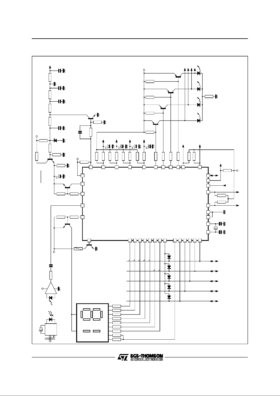
TYPICALAPPLICATION
Tuning
Voltage
C6
100nF
Ω
R16
82k
C5
100nF
Ω
R15
56k
C4
150nF
Ω
R14
33k
Ω
R13
33k
C2
100nF
High Voltage
R1
Z1
TAA550
Ω
R8
1%
1.6k
R9
5.6kΩ1%
T3
BC297
+5V
R5
6.8kΩ
(V) - 33V
H
V
R2
11mA
R2 = R1/4
R1 (kΩ)=
T4
BF259
Ω
R7
82k
C1
22µF
Ω
R6
4.7k
391920
R10
R11
M494
VHF I
VHF III
CATV
AV1
18
R33
UHF
2 x 5.6kΩ
R34
DL4DL3DL2DL1
AV0
17
R35
Ω
680
AFC DEF
OUT
R38R37
R36
Ω
5.6k
FB
+5V
Sync
MS1MS0
+12V
T9
BC177
R32
10kΩ
T8
BC177
R31
10kΩ
T7
BC177
R30
10kΩ
T5
BSX93
T6
CON
C10
28
BC177
R29
10kΩ
10µF
R25 8.2kΩ24R26 8.2kΩR27 8.2kΩ
R28 8.2kΩ
23
22
21
Ω
R12
3.3k
Ω
3.9k
1.5kΩ
VOL
SAT
LUM
C7
10µF
C8
10µF
C9
10µF
Ω
R17 22kΩ
R19 22kΩ
R21 22kΩ
R18 5.6kΩ
R20 5.6kΩ
R22 5.6k
27
34
33
R23 22kΩ
R24 5.6kΩ
31
+5V
500kHz
R39
4.7nF
Ω
2.2k
TDA8160
M708
R4
+5/12V
357
Ω
Ω
R3
1k
680
T2
BC177
16
Store Prog15Store Analog14TuneUp13TuneDown11BandSeq10PrgUp9PrgDown
D4
D3
D2
D1
D0
Relay
a
38
b
fh
abcdefghi
ce
d
i
M494
6
D5
D5
D5
D5
D5
85432
2 x 5.6kΩ
29 30
C12
100nF
Osc
25 4026 12 32 36 37
1
C11
100nF
21/22
494-24.EPS
Page 22

M494
PACKAGE MECHANICAL DATA
40 PINS- PLASTICPACKAGE
Dimensions
Min. Typ. Max. Min. Typ. Max.
Millimeters Inches
a1 0.63 0.025
b 0.45 0.018
b1 0.23 0.31 0.009 0.012
b2 1.27 0.050
D 52.58 2.070
E 15.2 16.68 0.598 0.657
e 2.54 0.100
e3 48.26 1.900
F 14.1 0.555
i 4.445 0.175
L 3.3 0.130
Information furnished is believed to be accurateand reliable. However, SGS-THOMSON Microelectronics assumes no responsibility
for the consequences of use of such information nor for any infringement of patents or otherrights of third parties which may result
from its use. No licence is granted byimplication or otherwise under any patent or patent rights of SGS-THOMSON Microelectronics.
Specifications mentioned in this publication are subject to change without notice. This publication supersedes and replaces all
information previously supplied. SGS-THOMSON Microelectronics products are not authorized for use as critical components in life
support devices or systems without express written approval of SGS-THOMSON Microelectronics.
1995 SGS-THOMSON Microelectronics - All Rights Reserved
Purchase of I
2
I
C Patent. Rights to use these components in a I2C system, is granted provided that the system conformsto
Australia - Brazil - China- France- Germany - Hong Kong - Italy - Japan- Korea - Malaysia - Malta - Morocco
The Netherlands -Singapore - Spain - Sweden - Switzerland - Taiwan - Thailand - United Kingdom -U.S.A.
2
C Components of SGS-THOMSON Microelectronics, conveys a license under the Philips
2
the I
C Standard Specifications as defined by Philips.
SGS-THOMSON Microelectronics GROUP OF COMPANIES
PM-DIP40.EPS
22/22
 Loading...