

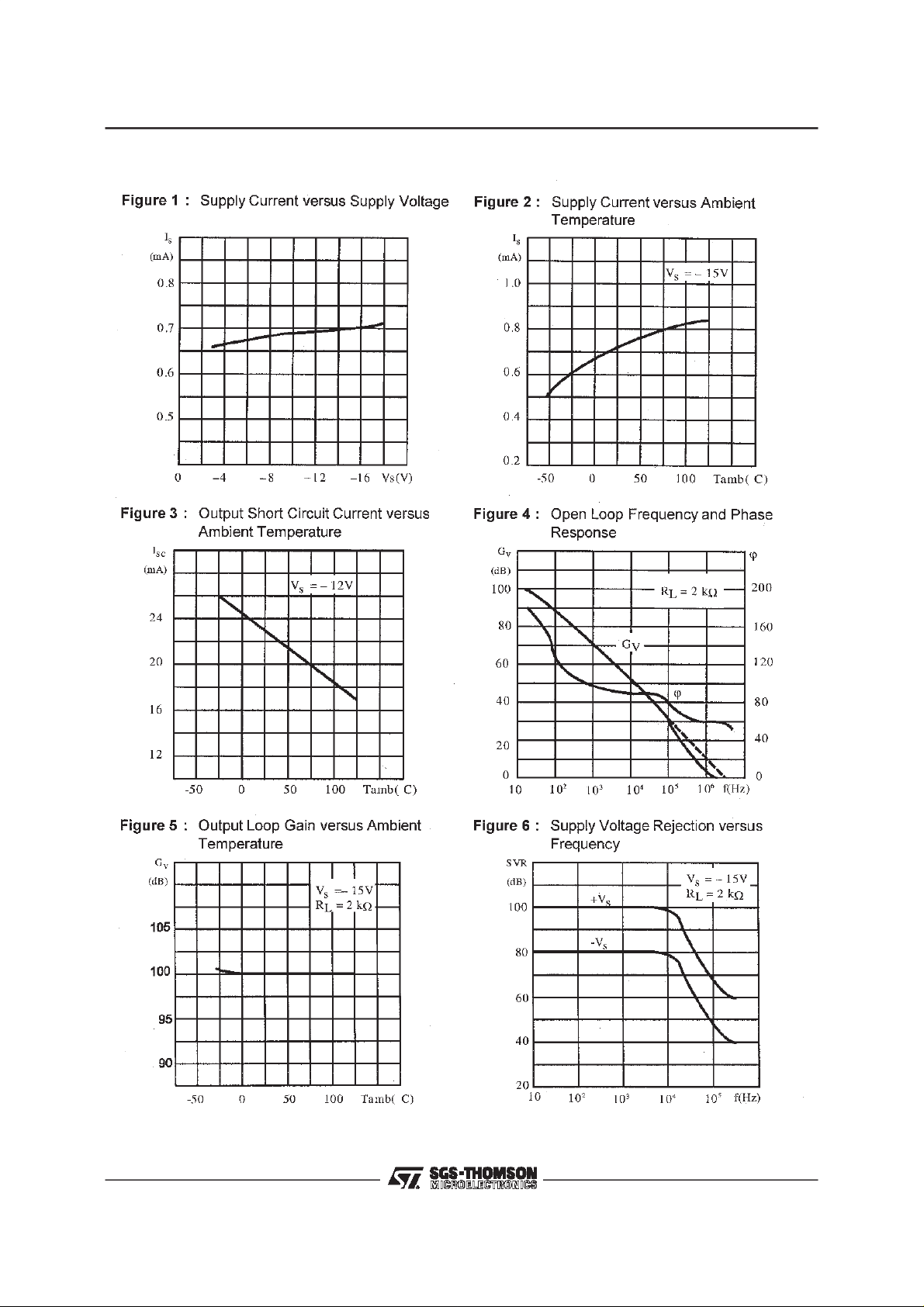
查询LS404供应商
.
SINGLEORSPLITSUPPLYOPERATION
.
LOW POWER CONSUMPTION
.
SHORT CIRCUIT PROTECTION
.
LOW DISTORTION,LOW NOISE
.
HIGHGAIN-BANDWIDTH PRODUCT
.
HIGHCHANNEL SEPARATION
LS404
HIGH PERFORMANCE
QUAD OPERATIONAL AMPLIFIERS
DESCRIPTION
The LS404is a high performancequadoperational
amplifier with frequency and phasecompensation
builtintothechip.Theinternalphasecompensation
allows stable operationas voltagefollowerin spite
of its high Gain-BandwidthProduct.
The circuit presents very stable electrical characteristics over the entire supply voltage range, and
it particularlyintendedforprofessionalandtelecom
applications(active filters, etc).
The patented input stage circuit allowssmall input
signal swings below the negative supply voltage
and preventsphase inversionwhen the inputs are
over drivers.
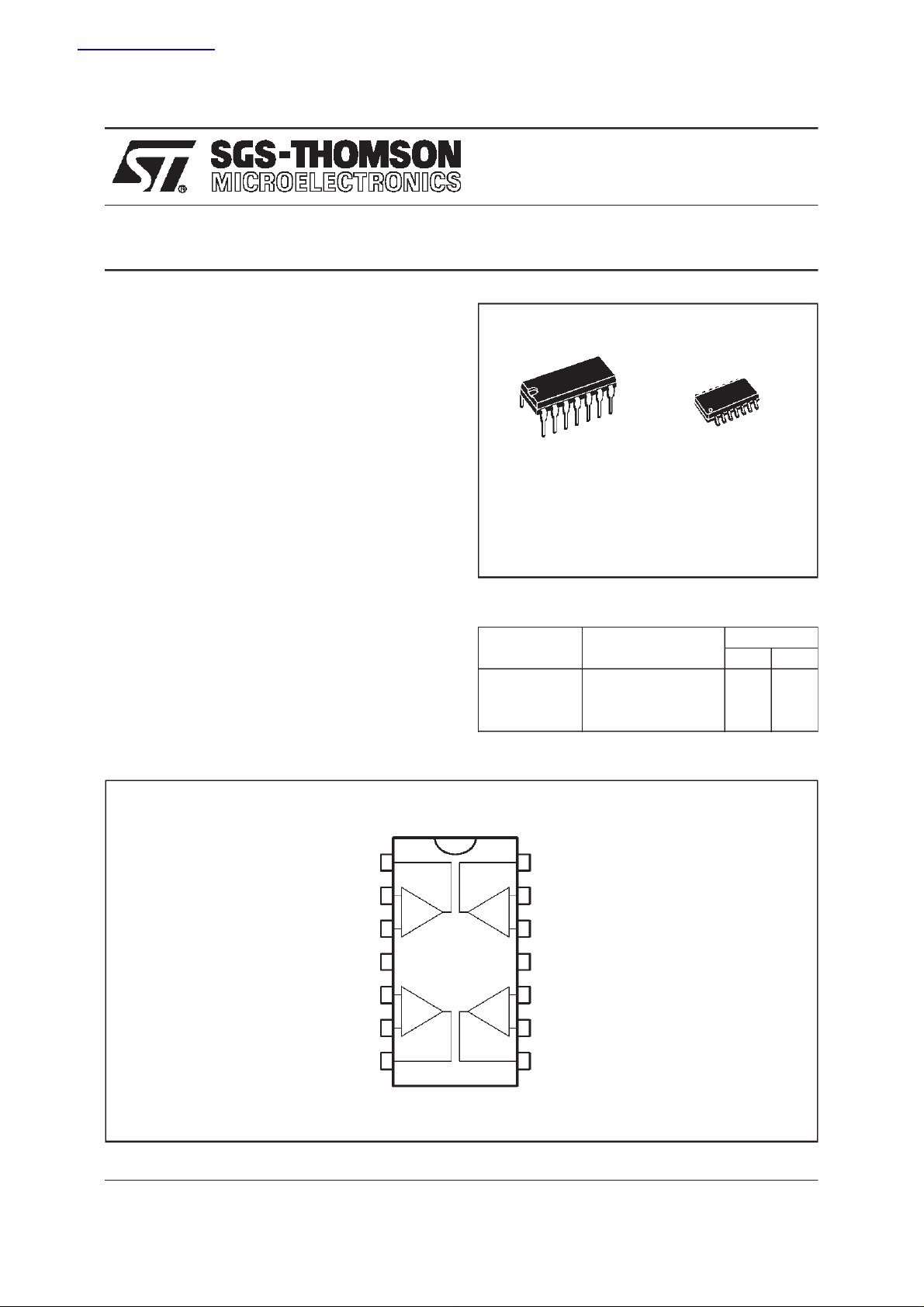
PINCONNECTIONS (topview)
Output 1
Inverting Input 1
Non-inverting Input 1
1
2
-
+
3
N
DIP14
(Plastic Package)
ORDER CODES
Part Number Temperature Range
LS404C 0
LS404I -40
LS404M -55
14
Output 4
Inverting Input 4
13
-
+
Non-inverting Input 4
12
(Plastic Micropackage)
o
C, +70oC ••
o
C, +105oC • ù
o
C, +125oC ••
D
SO14
Package
ND
December 1997
V
CC
Non-inverting Input 2
Inverting Input 2
Output 2
+
4
5
+
-
6
7
11
10
+
-
9
8
-
V
CC
Non-inverting Input 3
Inverting Input 3
Output 3
1/12
LS404
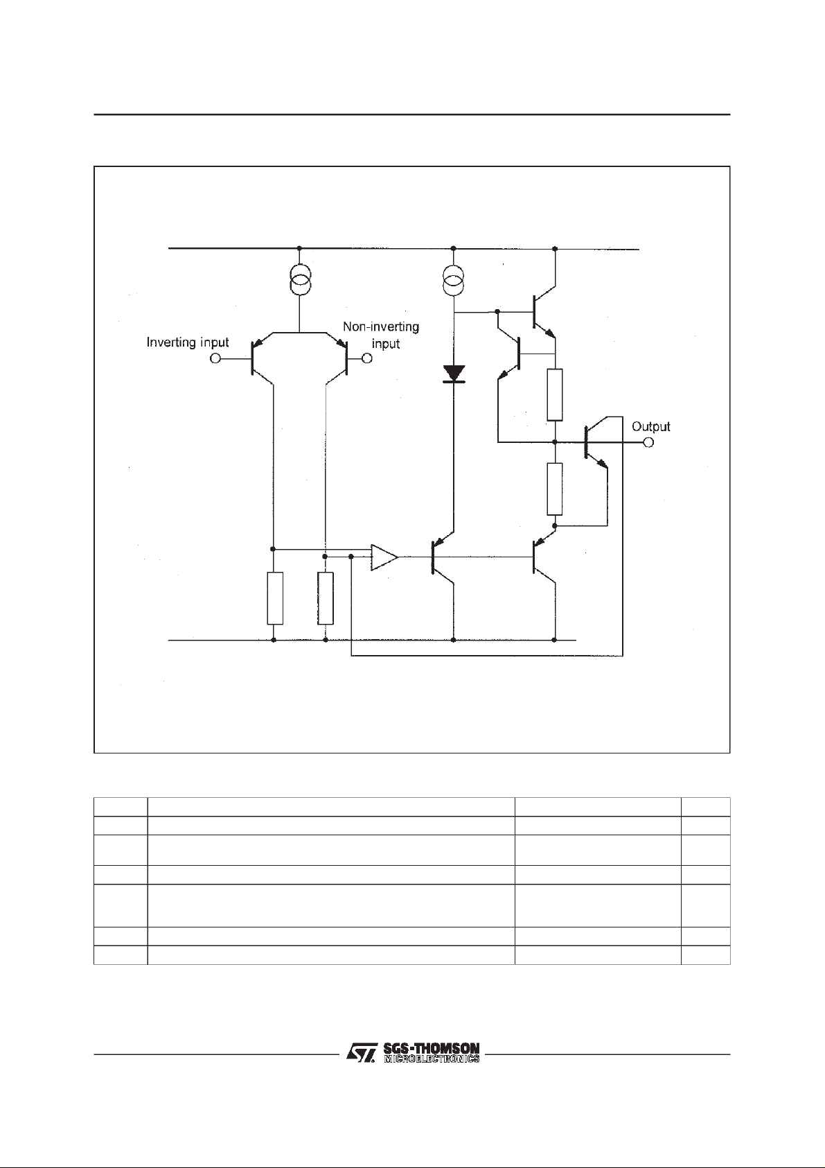
SCHEMATIC DIAGRAM (1/4LS404)
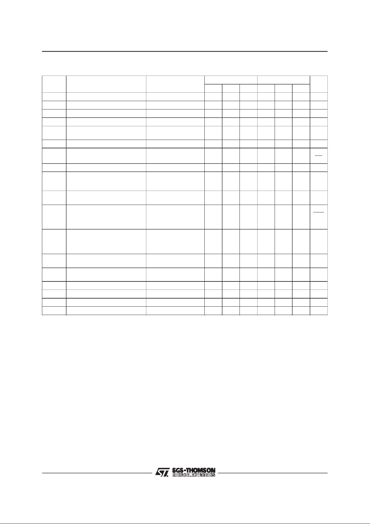
ABSOLUTEMAXIMUMRATINGS
Symbol Parameter Value Unit
V
T
2/12
Supply Voltage ±18 V
CC
Input Voltage (positive)
V
i
V
Differential Input Voltage ± (VCC-1)
id
Operating Temperature Range LS404C
oper
(negative)
LS404I
LS404M
P
Power Dissipation at T
tot
Storage Temperature -65to 150
T
stg
=70oC 400 mW
amb
+V
CC
-VCC- 0.5
0 to +70
-40 to +105
-55 to +125
V
o
C
o
C
LS404
ELECTRICALCHARACTERISTICS (VCC= ±15V,T
Symbol Parameter Test Conditions
Supply Current 1.3 2 1.5 3 mA
I
CC
Input Bias Current 50 200 100 300 nA
I
ib
Input Resistance f = 1kHz 1 1 MΩ
R
i
Input Offset Voltage Rs≤ 10kΩ 0.7 2.5 0.5 5 mV
V
io
DV
GBP Gain-Bandwidth Product f = 100kHz R
Input Offset Voltage Drift Rs≤ 10kΩ
io
I
Input Offset Current 10 40 20 80 nA
io
Input Offset Current Drift T
DI
io
Output Short Circuit Current 23 23 mA
I
os
Large Signal Voltage Gain RL=2kΩ VCC= ±15V
A
vd
.<Top<T
T
min
.<Top<T
min
V
C
e
Equivalent Input Noise Voltage f = 1kHz
n
R
R
R
s
s
s
=50Ω
=1kΩ
= 10kΩ
= 25oC, unless otherwise specified)
amb
LS404I - LM401M LS404C
Min. Typ. Max. Min. Typ. Max.
.5 5
max
. 0.08 0.1 nA
max
= ±4V 90 100
CC
=2k
L
= 100pF
L
1.8 3 1.5 2.5 MHz
95
8
10
18
86 100
95
15 10
12
20
THD Total Harmonic Distortion Unity Gain
=2kΩ,Vo=2V
R
±V
V
L
f = 1kHz
f = 20kHz
Output Voltage Swing RL=2kΩ VCC= ±15V
opp
Large Signal Voltage Swing f = 10kHz RL= 10kΩ
opp
V
CC
R
L
pp
= ±4V
=1kΩ
±13
0.01
0.03
±3
22
20
0.4 0.01
0.03
±13
±3
22
20
SR Slew Rate Unity Gain, RL=2kΩ 0.8 1.5 1 V/µs
CMR Common Mode Rejection Ratio V
SVR Supply Voltage Rejection Ratio V
V
O1/VO2
Channel Separation f = 1kHz 100 120 120 dB
= 10V 90 94 80 90 dB
ic
= 1V f = 100Hz 90 94 86 90 dB
ic
Unit
µV/
√
V
°C
dB
nV
Hz
%
V
PP
o
C
3/12
LS404
4/12
 Loading...