

现货库存、技术资料、百科信息、热点资讯,精彩尽在鼎好!
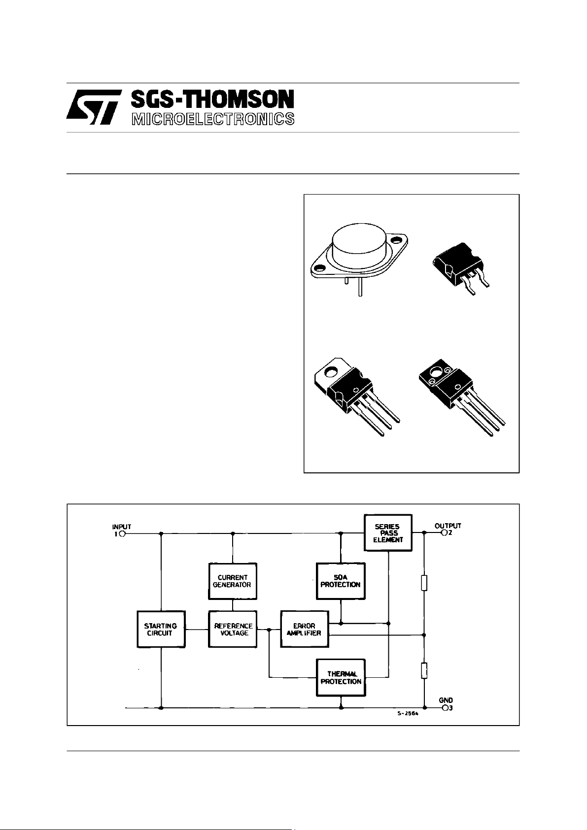
POSITIVE VOLTAGE REGULATORS
■ OUTPUTCURRENT UPTO 1.5 A
■ OUTPUTVOLTAGESOF 5; 5.2; 6; 8; 8.5;9;
12; 15; 18; 24V
■ THERMAL OVERLOADPROTECTION
■ SHORTCIRCUIT PROTECTION
■ OUTPUTTRANSITIONSOAPROTECTION
L7800
SERIES
DESCRIPTION
The L7800 series of three-terminal positive
regulators is available in TO-220 ISOWATT220
TO-3 and D
2
PAK packages and several fixed
output voltages, making it useful in a wide range
of applications.Theseregulatorscan provide local
on-card regulation, eliminating the distribution
problems associated with single point regulation.
Each type employs internal current limiting,
thermal shut-down and safe area protection,
making it essentially indestructible. If adequate
heat sinking is provided, they can deliver over 1A
output current. Although designed primarily as
fixed voltage regulators, these devices can be
used with external components to obtain
adjustablevoltages and currents.
BLOCK DIAGRAM
1
2
TO-3
3
2
1
TO-220 ISOWATT220
D2PAK
3
1
3
2
1
January 1997
1/25
L7800
ABSOLUTE MAXIMUMRATINGS
Symbol Parameter Value Unit
DC InputVoltage(forVO=5to18V)
V
i
OutputCurrent Internally limited
I
o
P
Power Dissipation Internally limited
tot
Operating Junction Temperature Range(for L7800)
T
op
(forV
= 20,24V)
O
(for L7800C)
T
StorageTemperature Range - 40 to 150
stg
THERMAL DATA
Symbol Parameter D2PAK TO-220 ISOWATT220 TO-3 Unit
R
thj-case
R
thj-amb
Thermal ResistanceJunction-case Max
Thermal ResistanceJunction-ambient Max
3
62.5
50
3
4
60
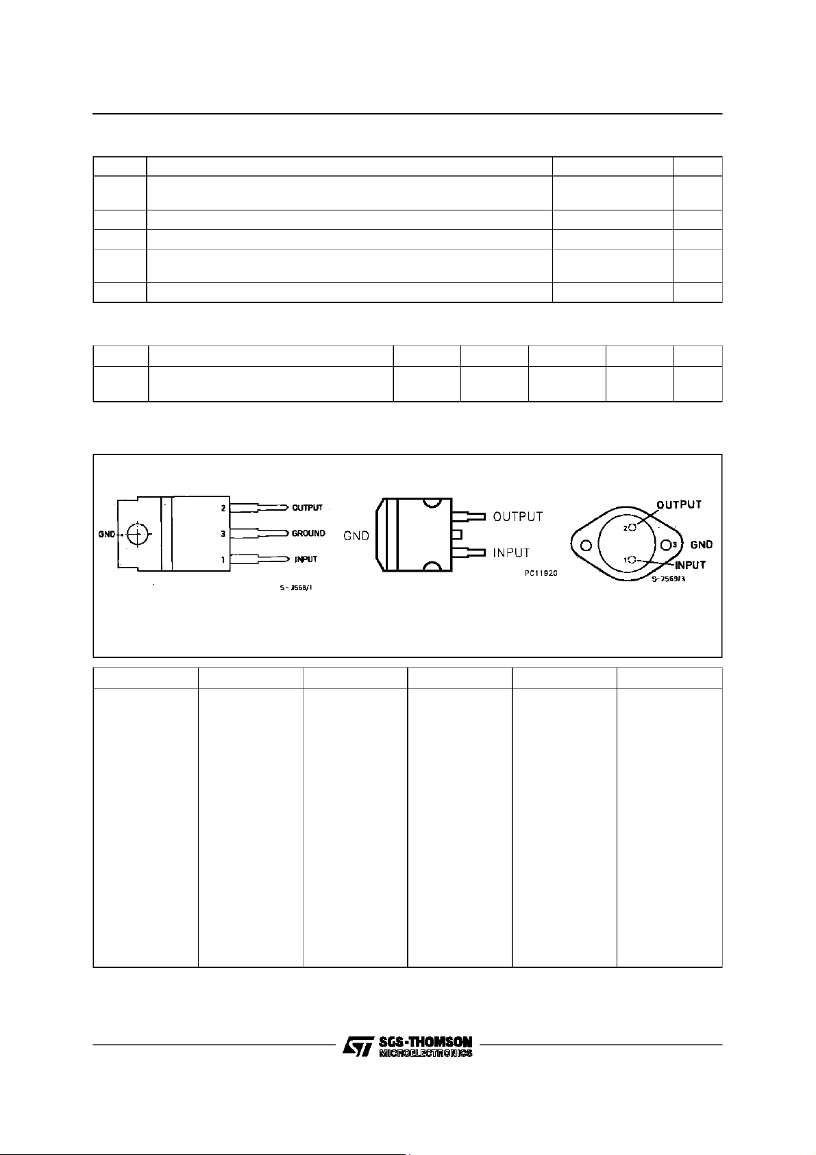
CONNECTION DIAGRAM AND ORDERINGNUMBERS (top view)
35
40
- 55 to 125
0to150
35
4
o
o
V
V
o
C
o
C
o
C
C/W
C/W
TO-220 & ISOWATT220 TO-3D2PAK
Type TO-220 D
2
L7805
L7805C
L7852C
L7805CV
L7852CV
L7805CD2T
L7852CD2T
L7806
L7806C
L7806CV
L7806CD2T
L7808
L7808C
L7885C
L7809C
L7808CV
L7885CV
L7809CV
L7808CD2T
L7885CD2T
L7809CD2T
L7812
L7812C
L7812CV
L7812CD2T
L7815
L7815C
L7815CV
L7815CD2T
L7818
L7818C
L7818CV
L7818CD2T
L7820
L7820C
L7820CV
L7820CD2T
L7824
L7824C
(*) AVAILABLE IN TAPE ANDREEL WITH ”-TR” SUFFIX
L7824CV
L7824CD2T
PAK (*) ISOWATT220 TO-3 Output Voltage
L7805CP
L7852CP
L7806CP
L7808CP
L7885CP
L7809CP
L7812CP
L7815CP
L7818CP
L7820CP
L7824CP
L7805T
L7805CT
L7852CT
L7806T
L7806CT
L7808T
L7808CT
L7885CT
L7809CT
L7812T
L7812CT
L7815T
L7815CT
L7818T
L7818CT
L7820T
L7820CT
L7824T
L7824CT
5V
5V
5.2V
6V
6V
8V
8V
8.5V
9V
12V
12V
15V
15V
18V
18V
20V
20V
24V
24V
2/25
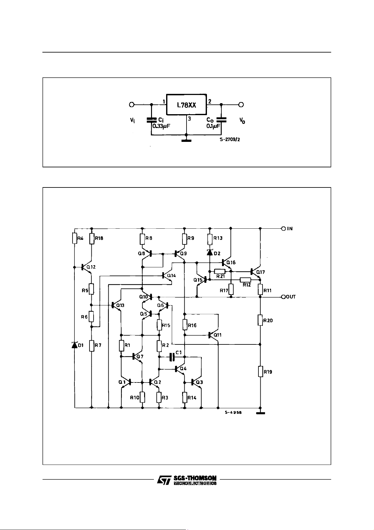
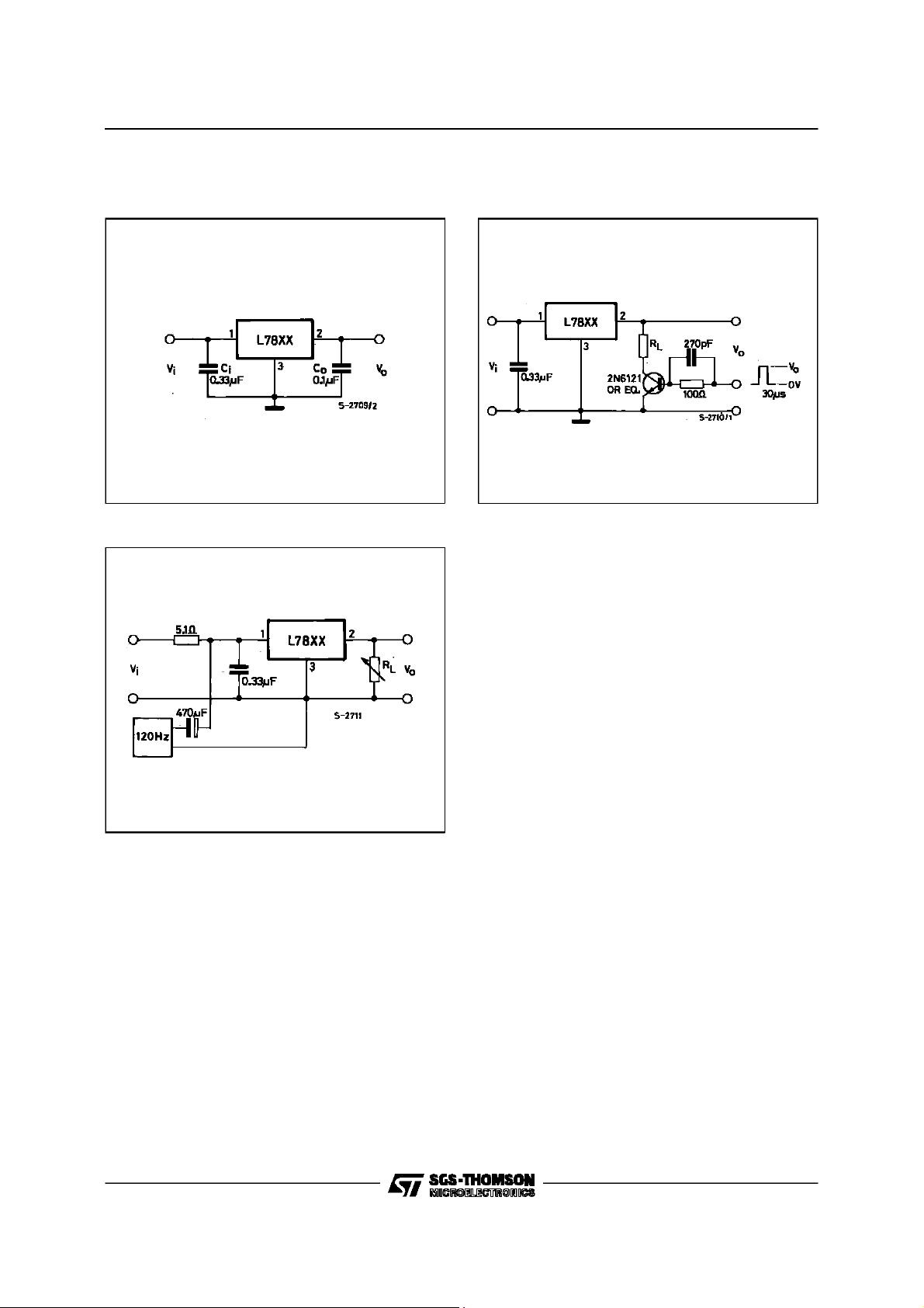
APPLICATIONCIRCUIT
SCHEMATICDIAGRAM
L7800
3/25
L7800
TEST CIRCUITS
Figure3 : Ripple Rejection.
Figure2 : Load Regulation.Figure1 : DC Parameter
4/25

L7800
ELECTRICALCHARACTERISTICS FOR L7805 (refer to the test circuits,Tj= -55 to 150oC,
=10V, Io=500 mA, Ci= 0.33 µF,Co= 0.1 µF unlessotherwise specified)
V
i
Symbol Parameter Test Conditions Min. Typ. Max. Unit
V
OutputVoltage Tj=25oC 4.855.2V
o
V
OutputVoltage Io= 5mA to1A Po≤ 15 W
o
* LineRegulation Vi=7to25V Tj=25oC
∆V
o
∆V
* LoadRegulation Io= 5 to1500 mA Tj=25oC
o
I
Quiescent Current Tj=25oC6mA
d
∆I
Quiescent Current Change Io= 5 to1000 mA 0.5 mA
d
∆I
Quiescent Current Change Vi=8to25V 0.8 mA
d
∆
V
OutputVoltage Drift Io=5mA 0.6 mV/oC
o
∆
T
eN OutputNoise Voltage B=10Hzto 100KHz T
=8 to20 V
V
i
=8to12V Tj=25oC
V
i
= 250 to750 mA Tj=25oC
I
o
=25oC40µV/V
j
SVR Supply VoltageRejection Vi=8 to18 V f = 120 Hz 68 dB
V
Dropout Voltage Io=1A Tj=25oC22.5V
d
R
OutputResistance f = 1 KHz 17 mΩ
o
I
ShortCircuit Current Vi=35V Tj=25oC 0.75 1.2 A
sc
I
ShortCircuit Peak Current Tj=25oC 1.3 2.2 3.3 A
scp
4.65 5 5.35 V
3
1
50
25
100
25
mV
mV
mV
mV
O
ELECTRICALCHARACTERISTICS FOR L7806 (refer to the test circuits, Tj= -55 to 150oC,
=15V, Io=500 mA, Ci= 0.33 µF,Co= 0.1 µF unlessotherwise specified)
V
i
Symbol Parameter Test Conditions Min. Typ. Max. Unit
V
OutputVoltage Tj=25oC 5.75 6 6.25 V
o
V
OutputVoltage Io= 5mA to1A Po≤ 15 W
o
* LineRegulation Vi=8to25V Tj=25oC
∆V
o
∆V
* LoadRegulation Io= 5 to1500mA Tj=25oC
o
I
Quiescent Current Tj=25oC6mA
d
∆I
Quiescent Current Change Io= 5 to1000 mA 0.5 mA
d
∆I
Quiescent Current Change Vi=9to25V 0.8 mA
d
∆
V
OutputVoltage Drift Io=5mA 0.7 mV/oC
o
∆
T
eN OutputNoise Voltage B=10Hzto 100KHz T
V
=9 to21 V
i
=9to13V Tj=25oC
V
i
= 250 to750 mA Tj=25oC
I
o
=25oC40µV/V
j
SVR Supply VoltageRejection Vi=9 to19 V f = 120 Hz 65 dB
V
Dropout Voltage Io=1A Tj=25oC22.5V
d
R
OutputResistance f = 1 KHz 19 mΩ
o
I
ShortCircuit Current Vi=35V Tj=25oC 0.75 1.2 A
sc
I
ShortCircuit Peak Current Tj=25oC 1.3 2.2 3.3 A
scp
* Load and line regulation are specified at constant junction temperature. Changes in Vodue to heating effects must be taken into account
separately. Pulce testing with low duty cycle isused.
5.65 6 6.35 V
60
30
100
30
mV
mV
mV
mV
O
5/25
L7800
ELECTRICALCHARACTERISTICS FOR L7808 (refer to the test circuits,Tj= -55 to 150oC,
=14V, Io=500 mA, Ci= 0.33 µF,Co= 0.1 µF unlessotherwise specified)
V
i
Symbol Parameter Test Conditions Min. Typ. Max. Unit
V
OutputVoltage Tj=25oC 7.788.3V
o
V
OutputVoltage Io= 5mA to1A Po≤ 15 W
o
* Line Regulation Vi=10.5 to 25 V Tj=25oC
∆V
o
∆V
* Load Regulation Io= 5 to1500 mA Tj=25oC
o
I
Quiescent Current Tj=25oC6mA
d
∆I
Quiescent Current Change Io= 5 to1000 mA 0.5 mA
d
∆I
Quiescent Current Change Vi=11.5 to 25 V 0.8 mA
d
∆
V
OutputVoltage Drift Io=5mA 1 mV/oC
o
∆
T
eN OutputNoise Voltage B=10Hzto 100KHz T
=11.5 to 23 V
V
i
=11to17V Tj=25oC
V
i
= 250 to750 mA Tj=25oC
I
o
=25oC40µV/V
j
SVR Supply Voltage Rejection Vi=11.5 to 21.5V f = 120 Hz 62 dB
V
Dropout Voltage Io=1A Tj=25oC22.5V
d
R
OutputResistance f = 1 KHz 16 mΩ
o
I
ShortCircuit Current Vi=35V Tj=25oC 0.75 1.2 A
sc
I
ShortCircuit Peak Current Tj=25oC 1.3 2.2 3.3 A
scp
7.688.4V
80
40
100
40
mV
mV
mV
mV
O
ELECTRICALCHARACTERISTICS FOR L7812 (refer to the test circuits,Tj= -55 to 150oC,
=19V, Io=500 mA, Ci= 0.33 µF,Co= 0.1 µF unlessotherwise specified)
V
i
Symbol Parameter Test Conditions Min. Typ. Max. Unit
V
OutputVoltage Tj=25oC 11.5 12 12.5 V
o
V
OutputVoltage Io= 5mA to1A Po≤ 15 W
o
* LineRegulation Vi=14.5 to 30 V Tj=25oC
∆V
o
∆V
* LoadRegulation Io= 5 to1500 mA Tj=25oC
o
I
Quiescent Current Tj=25oC6mA
d
∆I
Quiescent Current Change Io= 5 to1000 mA 0.5 mA
d
∆I
Quiescent Current Change Vi=15to30V 0.8 mA
d
∆
V
OutputVoltage Drift Io=5mA 1.5 mV/oC
o
∆
T
eN OutputNoise Voltage B=10Hzto 100KHz T
V
=15.5 to 27 V
i
=16to22V Tj=25oC
V
i
= 250 to750 mA Tj=25oC
I
o
=25oC40µV/V
j
SVR Supply VoltageRejection Vi=15to25V f=120Hz 61 dB
V
Dropout Voltage Io=1A Tj=25oC22.5V
d
R
OutputResistance f = 1 KHz 18 mΩ
o
I
ShortCircuit Current Vi=35V Tj=25oC 0.75 1.2 A
sc
I
ShortCircuit Peak Current Tj=25oC 1.3 2.2 3.3 A
scp
* Load and line regulation are specified at constant junction temperature. Changes in Vodue to heating effects must be taken into account
separately. Pulce testing with low duty cycle isused.
11.4 12 12.6 V
120
60
100
60
mV
mV
mV
mV
O
6/25

L7800
ELECTRICALCHARACTERISTICS FOR L7815 (refer to the test circuits,Tj= -55 to 150oC,
=23V, Io=500 mA, Ci= 0.33 µF,Co= 0.1 µF unlessotherwise specified)
V
i
Symbol Parameter Test Conditions Min. Typ. Max. Unit
V
OutputVoltage Tj=25oC 14.4 15 15.6 V
o
V
OutputVoltage Io= 5mA to1A Po≤ 15 W
o
* Line Regulation Vi=17.5 to 30 V Tj=25oC
∆V
o
∆V
* Load Regulation Io= 5 to1500 mA Tj=25oC
o
I
Quiescent Current Tj=25oC6mA
d
∆I
Quiescent Current Change Io= 5 to1000 mA 0.5 mA
d
∆I
Quiescent Current Change Vi=18.5 to 30 V 0.8 mA
d
∆
V
OutputVoltage Drift Io=5mA 1.8 mV/oC
o
∆
T
eN OutputNoise Voltage B=10Hzto 100KHz T
=18.5 to 30 V
V
i
=20to26V Tj=25oC
V
i
= 250 to750 mA Tj=25oC
I
o
=25oC40µV/V
j
SVR Supply Voltage Rejection Vi=18.5 to 28.5V f = 120 Hz 60 dB
V
Dropout Voltage Io=1A Tj=25oC22.5V
d
R
OutputResistance f = 1 KHz 19 mΩ
o
I
ShortCircuit Current Vi=35V Tj=25oC 0.75 1.2 A
sc
I
ShortCircuit Peak Current Tj=25oC 1.3 2.2 3.3 A
scp
14.251515.75 V
150
75
150
75
mV
mV
mV
mV
O
ELECTRICALCHARACTERISTICS FOR L7818 (refer to the test circuits,Tj= -55 to 150oC,
=26V, Io=500 mA, Ci= 0.33 µF,Co= 0.1 µF unlessotherwise specified)
V
i
Symbol Parameter Test Conditions Min. Typ. Max. Unit
V
OutputVoltage Tj=25oC 17.3 18 18.7 V
o
V
OutputVoltage Io= 5mA to1A Po≤ 15 W
o
* Line Regulation Vi=21to33V Tj=25oC
∆V
o
∆V
* Load Regulation Io= 5 to1500 mA Tj=25oC
o
I
Quiescent Current Tj=25oC6mA
d
∆I
Quiescent Current Change Io= 5 to1000 mA 0.5 mA
d
∆I
Quiescent Current Change Vi=22to33V 0.8 mA
d
∆
V
OutputVoltage Drift Io=5mA 2.3 mV/oC
o
∆
T
eN OutputNoise Voltage B=10Hzto 100KHz T
V
=22to33V
i
=24to30V Tj=25oC
V
i
= 250 to750 mA Tj=25oC
I
o
=25oC40µV/V
j
SVR Supply Voltage Rejection Vi=22to32V f=120Hz 59 dB
V
Dropout Voltage Io=1A Tj=25oC22.5V
d
R
OutputResistance f = 1 KHz 22 mΩ
o
I
ShortCircuit Current Vi=35V Tj=25oC 0.75 1.2 A
sc
I
ShortCircuit Peak Current Tj=25oC 1.3 2.2 3.3 A
scp
* Load and line regulation are specified at constant junction temperature. Changes in Vodue to heating effects must be taken into account
separately. Pulce testing with low duty cycle isused.
17.1 18 18.9 V
180
90
180
90
mV
mV
mV
mV
O
7/25

L7800
ELECTRICALCHARACTERISTICS FOR L7820 (refer to the test circuits,Tj= -55 to 150oC,
=28V, Io=500 mA, Ci= 0.33 µF,Co= 0.1 µF unlessotherwise specified)
V
i
Symbol Parameter Test Conditions Min. Typ. Max. Unit
V
OutputVoltage Tj=25oC 19.2 20 20.8 V
o
V
OutputVoltage Io= 5mA to1A Po≤ 15 W
o
* Line Regulation Vi=22.5 to 35 V Tj=25oC
∆V
o
∆V
* Load Regulation Io= 5 to1500 mA Tj=25oC
o
I
Quiescent Current Tj=25oC6mA
d
∆I
Quiescent Current Change Io= 5 to1000 mA 0.5 mA
d
∆I
Quiescent Current Change Vi=24to35V 0.8 mA
d
∆
V
OutputVoltage Drift Io=5mA 2.5 mV/oC
o
∆
T
eN OutputNoise Voltage B=10Hzto 100KHz T
=24to35V
V
i
=26to32V Tj=25oC
V
i
= 250 to750 mA Tj=25oC
I
o
=25oC40µV/V
j
SVR Supply Voltage Rejection Vi=24to35V f=120Hz 58 dB
V
Dropout Voltage Io=1A Tj=25oC22.5V
d
R
OutputResistance f = 1 KHz 24 mΩ
o
I
ShortCircuit Current Vi=35V Tj=25oC 0.75 1.2 A
sc
I
ShortCircuit Peak Current Tj=25oC 1.3 2.2 3.3 A
scp
19 20 21 V
200
100
200
100
mV
mV
mV
mV
O
ELECTRICALCHARACTERISTICS FOR L7824 (refer to the test circuits,Tj= -55 to 150oC,
=33V, Io=500 mA, Ci= 0.33 µF,Co= 0.1 µF unlessotherwise specified)
V
i
Symbol Parameter Test Conditions Min. Typ. Max. Unit
V
OutputVoltage Tj=25oC 232425 V
o
V
OutputVoltage Io= 5mA to1A Po≤ 15 W
o
* Line Regulation Vi=27to38V Tj=25oC
∆V
o
∆V
* Load Regulation Io= 5 to1500 mA Tj=25oC
o
I
Quiescent Current Tj=25oC6mA
d
∆I
Quiescent Current Change Io= 5 to1000 mA 0.5 mA
d
∆I
Quiescent Current Change Vi=28to38V 0.8 mA
d
∆
V
OutputVoltage Drift Io=5mA 3 mV/oC
o
∆
T
eN OutputNoise Voltage B=10Hzto 100KHz T
V
=28to38V
i
=30to36V Tj=25oC
V
i
= 250 to750 mA Tj=25oC
I
o
=25oC40µV/V
j
SVR Supply Voltage Rejection Vi=28to38V f=120Hz 56 dB
V
Dropout Voltage Io=1A Tj=25oC22.5V
d
R
OutputResistance f = 1 KHz 28 mΩ
o
I
ShortCircuit Current Vi=35V Tj=25oC 0.75 1.2 A
sc
I
ShortCircuit Peak Current Tj=25oC 1.3 2.2 3.3 A
scp
* Load and line regulation are specified at constant junction temperature. Changes in Vodue to heating effects must be taken into account
separately. Pulce testing with low duty cycle isused.
22.8 24 25.2 V
240
120
240
120
mV
mV
mV
mV
O
8/25

L7800
ELECTRICALCHARACTERISTICS FOR L7805C (refer to the test circuits,Tj= 0 to 125oC,
=10V, Io=500 mA, Ci= 0.33 µF,Co= 0.1 µF unlessotherwise specified)
V
i
Symbol Parameter Test Conditions Min. Typ. Max. Unit
V
OutputVoltage Tj=25oC 4.855.2V
o
V
OutputVoltage Io= 5mA to1A Po≤ 15 W
o
* Line Regulation Vi=7to25V Tj=25oC
∆V
o
∆V
* Load Regulation Io= 5 to1500 mA Tj=25oC
o
I
Quiescent Current Tj=25oC8mA
d
∆I
Quiescent Current Change Io= 5 to1000 mA 0.5 mA
d
∆I
Quiescent Current Change Vi=7to25V 0.8 mA
d
∆
V
OutputVoltage Drift Io= 5mA -1.1 mV/oC
o
∆
T
=7 to20 V
V
i
=8to12V Tj=25oC
V
i
= 250 to750 mA Tj=25oC
I
o
eN OutputNoise Voltage B=10Hzto 100KHz T
SVR Supply Voltage Rejection V
V
Dropout Voltage Io=1A Tj=25oC2V
d
R
OutputResistance f = 1 KHz 17 mΩ
o
I
ShortCircuit Current Vi=35V Tj=25oC 750 m A
sc
I
ShortCircuit Peak Current Tj=25oC2.2A
scp
=8 to18 V f = 120 Hz 62 dB
i
=25oC40µV
j
4.75 5 5.25 V
3
1
100
50
100
50
mV
mV
mV
mV
ELECTRICALCHARACTERISTICS FOR L7852C (refer to the test circuits,Tj= 0 to 125oC, Vi=10V,
= 500 mA, Ci=0.33 µF,Co=0.1 µF unless otherwise specified)
I
o
Symbol Parameter Test Conditions Min. Typ. Max. Unit
V
OutputVoltage Tj=25oC 5.0 5.2 5.4 V
o
V
OutputVoltage Io= 5mA to1A Po≤ 15 W
o
* Line Regulation Vi=7to25V Tj=25oC
∆V
o
∆V
* Load Regulation Io= 5 to1500 mA Tj=25oC
o
I
Quiescent Current Tj=25oC8mA
d
∆I
Quiescent Current Change Io= 5 to1000 mA 0.5 mA
d
∆I
Quiescent Current Change Vi=7to25V 1.3 mA
d
∆
V
OutputVoltage Drift Io= 5mA -1.0 mV/oC
o
∆
T
eN OutputNoise Voltage B=10Hzto 100KHz T
SVR Supply Voltage Rejection V
V
Dropout Voltage Io=1A Tj=25oC2V
d
R
OutputResistance f = 1 KHz 17 mΩ
o
I
ShortCircuit Current Vi=35V Tj=25oC 750 m A
sc
I
ShortCircuit Peak Current Tj=25oC2.2A
scp
* Load and line regulation are specified at constant junction temperature. Changes in Vodue to heating effects must be taken into account
separately. Pulce testing with low duty cycle isused.
V
=8 to20 V
i
=8to12V Tj=25oC
V
i
= 250 to750 mA Tj=25oC
I
o
=25oC42µV
j
=8 to18 V f = 120 Hz 61 dB
i
4.95 5.2 5.45 V
3
1
105
52
105
52
mV
mV
mV
mV
9/25

L7800
ELECTRICALCHARACTERISTICS FOR L7806C (refer to the test circuits,Tj= 0 to 125oC,
=11V, Io=500 mA, Ci= 0.33 µF,Co= 0.1 µF unlessotherwise specified)
V
i
Symbol Parameter Test Conditions Min. Typ. Max. Unit
V
OutputVoltage Tj=25oC 5.75 6 6.25 V
o
V
OutputVoltage Io= 5mA to1A Po≤ 15 W
o
* Line Regulation Vi=8to25V Tj=25oC
∆V
o
∆V
* Load Regulation Io= 5 to1500 mA Tj=25oC
o
I
Quiescent Current Tj=25oC8mA
d
∆I
Quiescent Current Change Io= 5 to1000 mA 0.5 mA
d
∆I
Quiescent Current Change Vi=8to25V 1.3 mA
d
∆
V
OutputVoltage Drift Io= 5mA -0.8 mV/oC
o
∆
T
=8 to21 V
V
i
=9to13V Tj=25oC
V
i
= 250 to750 mA Tj=25oC
I
o
eN OutputNoise Voltage B=10Hzto 100KHz T
SVR Supply Voltage Rejection V
V
Dropout Voltage Io=1A Tj=25oC2V
d
R
OutputResistance f = 1 KHz 19 mΩ
o
I
ShortCircuit Current Vi=35V Tj=25oC 550 m A
sc
I
ShortCircuit Peak Current Tj=25oC2.2A
scp
=9 to19 V f = 120 Hz 59 dB
i
=25oC45µV
j
5.766.3V
120
60
120
60
mV
mV
mV
mV
ELECTRICALCHARACTERISTICS FOR L7808C (refer to the test circuits,Tj= 0 to 125oC, Vi=14V,
= 500 mA, Ci=0.33 µF,Co=0.1 µF unless otherwise specified)
I
o
Symbol Parameter Test Conditions Min. Typ. Max. Unit
V
OutputVoltage Tj=25oC 7.788.3V
o
V
OutputVoltage Io= 5mA to1A Po≤ 15 W
o
* Line Regulation Vi=10.5 to 25 V Tj=25oC
∆V
o
∆V
* Load Regulation Io= 5 to1500 mA Tj=25oC
o
I
Quiescent Current Tj=25oC8mA
d
∆I
Quiescent Current Change Io= 5 to1000 mA 0.5 mA
d
∆I
Quiescent Current Change Vi=10.5 to 25 V 1 mA
d
∆
V
OutputVoltage Drift Io= 5mA -0.8 mV/oC
o
∆
T
eN OutputNoise Voltage B=10Hzto 100KHz T
SVR Supply Voltage Rejection V
V
Dropout Voltage Io=1A Tj=25oC2V
d
R
OutputResistance f = 1 KHz 16 mΩ
o
I
ShortCircuit Current Vi=35V Tj=25oC 450 m A
sc
I
ShortCircuit Peak Current Tj=25oC2.2A
scp
* Load and line regulation are specified at constant junction temperature. Changes in Vodue to heating effects must be taken into account
separately. Pulce testing with low duty cycle isused.
V
=10.5 to 25 V
i
=11to17V Tj=25oC
V
i
= 250 to750 mA Tj=25oC
I
o
=25oC52µV
j
=11.5 to 21.5V f = 120 Hz 56 dB
i
7.688.4V
160
80
160
80
mV
mV
mV
mV
10/25

L7800
ELECTRICALCHARACTERISTICS FOR L7885C (refer to the test circuits,Tj= 0 to 125oC, Vi=
14.5V,I
Symbol Parameter Test Conditions Min. Typ. Max. Unit
∆V
∆V
SVR Supply Voltage Rejection V
=500 mA, Ci=0.33 µF, Co=0.1 µF unless otherwise specified)
o
V
OutputVoltage Tj=25oC 8.2 8.5 8.8 V
o
V
OutputVoltage Io= 5mA to1A Po≤ 15 W
o
* Line Regulation Vi=11to27V Tj=25oC
o
* Load Regulation Io= 5 to1500 mA Tj=25oC
o
I
Quiescent Current Tj=25oC8mA
d
∆I
Quiescent Current Change Io= 5 to1000 mA 0.5 mA
d
∆I
Quiescent Current Change Vi=11to27V 1 mA
d
∆
V
OutputVoltage Drift Io= 5mA -0.8 mV/oC
o
∆
T
eN OutputNoise Voltage B=10Hzto 100KHz T
V
Dropout Voltage Io=1A Tj=25oC2V
d
R
OutputResistance f = 1 KHz 16 mΩ
o
I
ShortCircuit Current Vi=35V Tj=25oC 450 m A
sc
I
ShortCircuit Peak Current Tj=25oC2.2A
scp
=11to26V
V
i
=11.5 to 17.5V Tj=25oC
V
i
= 250 to750 mA Tj=25oC
I
o
=25oC55µV
j
=12to22V f=120Hz 56 dB
i
8.1 8.5 8. 9 V
160
80
160
80
mV
mV
mV
mV
ELECTRICALCHARACTERISTICS FOR L7809C (refer to the test circuits,Tj= 0 to 125oC, Vi=15V,
= 500 mA, Ci=0.33 µF,Co=0.1 µF unless otherwise specified)
I
o
Symbol Parameter Test Conditions Min. Typ. Max. Unit
V
OutputVoltage Tj=25oC 8.65 9 9.35 V
o
V
OutputVoltage Io= 5mA to1A Po≤ 15 W
o
* Line Regulation Vi=11.5 to 26 V Tj=25oC
∆V
o
∆V
* Load Regulation Io= 5 to1500 mA Tj=25oC
o
I
Quiescent Current Tj=25oC8mA
d
∆I
Quiescent Current Change Io= 5 to1000 mA 0.5 mA
d
∆I
Quiescent Current Change Vi=11.5 to 26 V 1 mA
d
∆
V
OutputVoltage Drift Io= 5mA -1.0 mV/oC
o
∆
T
eN OutputNoise Voltage B=10Hzto 100KHz T
SVR Supply Voltage Rejection V
V
Dropout Voltage Io=1A Tj=25oC2V
d
R
OutputResistance f = 1 KHz 17 mΩ
o
I
ShortCircuit Current Vi=35V Tj=25oC 400 m A
sc
I
ShortCircuit Peak Current Tj=25oC2.2A
scp
* Load and line regulation are specified at constant junction temperature. Changes in Vodue to heating effects must be taken into account
separately. Pulce testing with low duty cycle isused.
V
=11.5 to 26 V
i
=12to18V Tj=25oC
V
i
= 250 to750 mA Tj=25oC
I
o
=25oC70µV
j
=12to23V f=120Hz 55 dB
i
8.55 9 9.45 V
180
90
180
90
mV
mV
mV
mV
11/25

L7800
ELECTRICALCHARACTERISTICS FOR L7812C (refer to the test circuits,Tj= 0 to 125oC, Vi=19V,
= 500 mA, Ci=0.33 µF,Co=0.1 µF unless otherwise specified)
I
o
Symbol Parameter Test Conditions Min. Typ. Max. Unit
V
OutputVoltage Tj=25oC 11.5 12 12.5 V
o
V
OutputVoltage Io= 5mA to1A Po≤ 15 W
o
* Line Regulation Vi=14.5 to 30 V Tj=25oC
∆V
o
∆V
* Load Regulation Io= 5 to1500 mA Tj=25oC
o
I
Quiescent Current Tj=25oC8mA
d
∆I
Quiescent Current Change Io= 5 to1000 mA 0.5 mA
d
∆I
Quiescent Current Change Vi=14.5 to 30 V 1 mA
d
∆
V
OutputVoltage Drift Io= 5mA -1 mV/oC
o
∆
T
=14.5 to 27 V
V
i
=16to22V Tj=25oC
V
i
= 250 to750 mA Tj=25oC
I
o
eN OutputNoise Voltage B=10Hzto 100KHz T
SVR Supply Voltage Rejection V
V
Dropout Voltage Io=1A Tj=25oC2V
d
R
OutputResistance f = 1 KHz 18 mΩ
o
I
ShortCircuit Current Vi=35V Tj=25oC 350 m A
sc
I
ShortCircuit Peak Current Tj=25oC2.2A
scp
=15to25V f=120Hz 55 dB
i
=25oC75µV
j
11.4 12 12.6 V
240
120
240
120
mV
mV
mV
mV
ELECTRICALCHARACTERISTICS FOR L7815C (refer to the test circuits,Tj= 0 to 125oC, Vi=23V,
= 500 mA, Ci=0.33 µF,Co=0.1 µF unless otherwise specified)
I
o
Symbol Parameter Test Conditions Min. Typ. Max. Unit
V
OutputVoltage Tj=25oC 14.4 15 15.6 V
o
V
OutputVoltage Io= 5mA to1A Po≤ 15 W
o
* Line Regulation Vi=17.5 to 30 V Tj=25oC
∆V
o
∆V
* Load Regulation Io= 5 to1500 mA Tj=25oC
o
I
Quiescent Current Tj=25oC8mA
d
∆I
Quiescent Current Change Io= 5 to1000 mA 0.5 mA
d
∆I
Quiescent Current Change Vi=17.5 to 30 V 1 mA
d
∆
V
OutputVoltage Drift Io= 5mA -1 mV/oC
o
∆
T
eN OutputNoise Voltage B=10Hzto 100KHz T
SVR Supply Voltage Rejection V
V
Dropout Voltage Io=1A Tj=25oC2V
d
R
OutputResistance f = 1 KHz 19 mΩ
o
I
ShortCircuit Current Vi=35V Tj=25oC 230 m A
sc
I
ShortCircuit Peak Current Tj=25oC2.1A
scp
* Load and line regulation are specified at constant junction temperature. Changes in Vodue to heating effects must be taken into account
separately. Pulce testing with low duty cycle isused.
V
=17.5 to 30 V
i
=20to26V Tj=25oC
V
i
= 250 to750 mA Tj=25oC
I
o
=25oC90µV
j
=18.5 to 28.5V f = 120 Hz 54 dB
i
14.251515.75 V
300
150
300
150
mV
mV
mV
mV
12/25

L7800
ELECTRICALCHARACTERISTICS FOR L7818C (refer to the test circuits,Tj= 0 to 125oC, Vi=26V,
= 500 mA, Ci=0.33 µF,Co=0.1 µF unless otherwise specified)
I
o
Symbol Parameter Test Conditions Min. Typ. Max. Unit
V
OutputVoltage Tj=25oC 17.3 18 18.7 V
o
V
OutputVoltage Io= 5mA to1A Po≤ 15 W
o
* Line Regulation Vi=21to33V Tj=25oC
∆V
o
∆V
* Load Regulation Io= 5 to1500 mA Tj=25oC
o
I
Quiescent Current Tj=25oC8mA
d
∆I
Quiescent Current Change Io= 5 to1000 mA 0.5 mA
d
∆I
Quiescent Current Change Vi=21to33V 1 mA
d
∆
V
OutputVoltage Drift Io= 5mA -1 mV/oC
o
∆
T
=21to33V
V
i
=24to30V Tj=25oC
V
i
= 250 to750 mA Tj=25oC
I
o
eN OutputNoise Voltage B=10Hzto 100KHz T
SVR Supply Voltage Rejection V
V
Dropout Voltage Io=1A Tj=25oC2V
d
R
OutputResistance f = 1 KHz 22 mΩ
o
I
ShortCircuit Current Vi=35V Tj=25oC 200 m A
sc
I
ShortCircuit Peak Current Tj=25oC2.1A
scp
=22to32V f=120Hz 53 dB
i
=25oC 110 µV
j
17.1 18 18.9 V
360
180
360
180
mV
mV
mV
mV
ELECTRICALCHARACTERISTICS FOR L7820C (refer to the test circuits,Tj= 0 to 125oC, Vi=28V,
= 500 mA, Ci=0.33 µF,Co=0.1 µF unless otherwise specified)
I
o
Symbol Parameter Test Conditions Min. Typ. Max. Unit
V
OutputVoltage Tj=25oC 19.2 20 20.8 V
o
V
OutputVoltage Io= 5mA to1A Po≤ 15 W
o
* Line Regulation Vi=22.5 to 35 V Tj=25oC
∆V
o
∆V
* Load Regulation Io= 5 to1500 mA Tj=25oC
o
I
Quiescent Current Tj=25oC8mA
d
∆I
Quiescent Current Change Io= 5 to1000 mA 0.5 mA
d
∆I
Quiescent Current Change Vi=23to35V 1 mA
d
∆
V
OutputVoltage Drift Io= 5mA -1 mV/oC
o
∆
T
eN OutputNoise Voltage B=10Hzto 100KHz T
SVR Supply Voltage Rejection V
V
Dropout Voltage Io=1A Tj=25oC2V
d
R
OutputResistance f = 1 KHz 24 mΩ
o
I
ShortCircuit Current Vi=35V Tj=25oC 180 m A
sc
I
ShortCircuit Peak Current Tj=25oC2.1A
scp
* Load and line regulation are specified at constant junction temperature. Changes in Vodue to heating effects must be taken into account
separately. Pulce testing with low duty cycle isused.
V
=23to35V
i
=26to32V Tj=25oC
V
i
= 250 to750 mA Tj=25oC
I
o
=25oC 150 µV
j
=24to35V f=120Hz 52 dB
i
19 20 21 V
400
200
400
200
mV
mV
mV
mV
13/25

L7800
ELECTRICALCHARACTERISTICS FOR L7824C (refer to the test circuits,Tj= 0 to 125oC, Vi=33V,
= 500 mA, Ci=0.33 µF,Co=0.1 µF unless otherwise specified)
I
o
Symbol Parameter Test Conditions Min. Typ. Max. Unit
V
OutputVoltage Tj=25oC 232425 V
o
V
OutputVoltage Io= 5mA to1A Po≤ 15 W
o
* Line Regulation Vi=27to38V Tj=25oC
∆V
o
∆V
* Load Regulation Io= 5 to1500 mA Tj=25oC
o
I
Quiescent Current Tj=25oC8mA
d
∆I
Quiescent Current Change Io= 5 to1000 mA 0.5 mA
d
∆I
Quiescent Current Change Vi=27to38V 1 mA
d
∆
V
OutputVoltage Drift Io= 5mA -1.5 mV/oC
o
∆
T
eN OutputNoise Voltage B=10Hzto 100KHz T
SVR Supply Voltage Rejection V
V
Dropout Voltage Io=1A Tj=25oC2V
d
R
OutputResistance f = 1 KHz 28 mΩ
o
I
ShortCircuit Current Vi=35V Tj=25oC 150 m A
sc
I
ShortCircuit Peak Current Tj=25oC2.1A
scp
* Load and line regulation are specified at constant junction temperature. Changes in Vodue to heating effects must be taken into account
separately. Pulce testing with low duty cycle isused.
=27to38V
V
i
=30to36V Tj=25oC
V
i
= 250 to750 mA Tj=25oC
I
o
=25oC 170 µV
j
=28to38V f=120Hz 50 dB
i
22.8 24 25.2 V
480
240
480
240
mV
mV
mV
mV
14/25

L7800
Figure4 : DropoutVoltage vs. Junction
Temperature.
Figure6 : Supply Voltage Rejectionvs.
Frequency.
Figure 5 : Peak Output Currentvs. Input/output
DifferentialVoltage.
Figure 7 : Output Voltage vs. Junction
Temperature.
Figure8 : Output Impedance vs. Frequency. Figure 9 : Quiescent Current vs. Junction
Temperature.
15/25
L7800
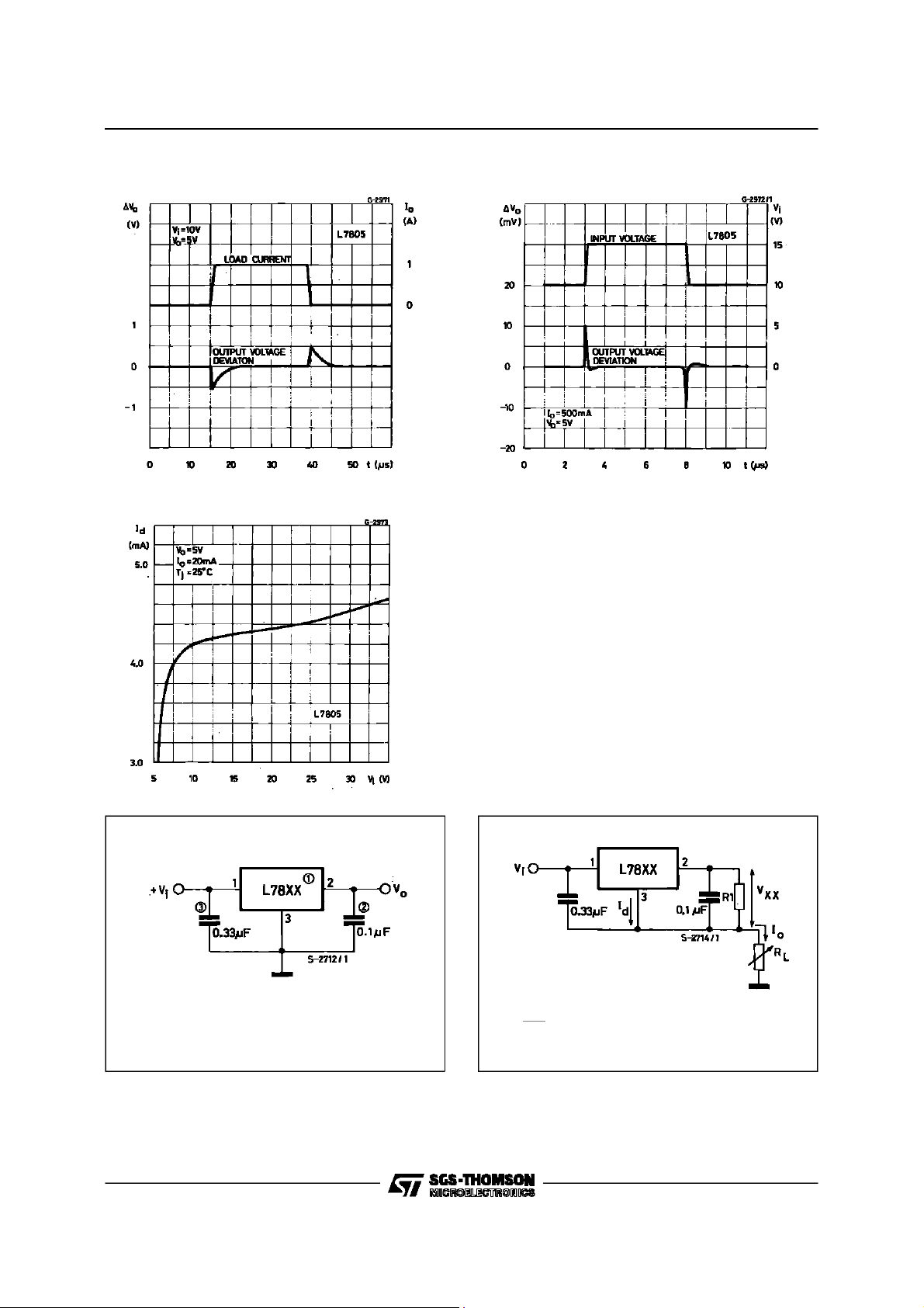
Figure10 : Load Transient Response. Figure 11 : Line TransientResponse.
Figure12 : QuiescentCurrentvs. Input
Voltage.
Figure13 : Fixed Output Regulator. Figure 14 : Current Regulator.
V
XX
=
+
I
d
R
1
NOTE:
1. To specify an outputvoltage, substitute voltage value for ”XX”.
2. Although no output capacitor is need for stability, it does
improve transient response.
3. Required if cregulator is locate an appreciable distance from
power supply filter.
16/25
I
O

L7800
Figure15 : Circuit for Increasing Output
Voltage.
IR1≥ 5I
d
R
VO=
V
XX
(1 +
2
)+
IdR
R
1
2
Figure 16 : Adjustable OutputRegulator
(7 to 30V).
Figure17 : 0.5 to 10V Regulator. Figure 18 : High CurrentVoltageRegulator.
VO =
V
BEQ
R1=
R
4
V
XX
R
1
IO=
1
I
Q
REQ
1
−
β
Q
1
V
BEQ
+
Q
(
I
1
REG
1
−
)
R
1
I
I
REG
17/25

L7800
Figure19 : High Output Current with Short
Figure 20 : Tracking Voltage Regulator.
CircuitProtection.
V
BEQ
2
=
R
SC
I
SC
Figure21 : Split Power Supply (± 15V – 1A). Figure 22 : NegativeOutput Voltage Circuit.
* Against potential latch-upproblems.
Figure23 : Switching Regulator. Figure 24 : High Input VoltageCircuit.
VIN=Vi-(VZ+VBE)
18/25

L7800
Figure25 : High Input VoltageCircuit. Figure 26 : High OutputVoltageRegulator.
Figure27 : High Input and Output Voltage. Figure 28 : Reducing PowerDissipation with
Dropping Resistor.
VO=VXX+V
Z1
Figure29 : Remote Shutdown.
R=
V
−
V
−
O(max
V
XX
DROP(max
+
I
)
d(max
)
)
i(min
)
I
19/25

L7800
Figure30 : Power AM Modulator(unityvoltage
gain,I
NOTE: The circuitperforms well up to 100KHz NOTE: Q2is connected as a diode in order to compensate the
Figure32 : Light Controllers (V
<1A).
o
o min=Vxx+VBE
).
Figure 31 : AdjustableOutputVoltage with
TemperatureCompensation.
R
V
=
V
O
variation of the Q
time ofthe V
o
XX
2
(1 +
)+
V
BE
R
1
with the temperature. C allows a slow rise-
1VBE
V
falls when the lightgoes up
O
Figure33 : Protectionagainst InputShort-circuit
withHighCapacitanceLoads.
20/25
V
rises when the lightgoes up
O
Application with high capacitance loads and an output voltage
greater than 6 volts need an external diode (see fig. 33) to protect
the deviceagainst input short circuit. In this case the input voltage
falls rapidly while the output voltage decrease slowly. The
capacitance dischrges by means of the Base-Emitter junction of
the series pass transistor in the regulator. If the energy is
sufficently high, the transistor may be destroyed. The external
diode by-passes the current from the IC toground.

TO-3 (R) MECHANICAL DATA
L7800
DIM.
mm inch
MIN. TYP. MAX. MIN. TYP. MAX.
A 11.7 0.460
B 0.96 1.10 0.037 0.043
C 1.70 0.066
D 8.7 0.342
E 20.0 0.787
G 10.9 0.429
N 16.9 0.665
P 26.2 1.031
R 3.88 4.09 0.152 0.161
U 39.50 1.555
V 30.10 1.185
P
G
U
V
N
O
R
B
DA
C
E
P003N
21/25

L7800
TO-220 MECHANICAL DATA
DIM.
MIN. TYP. MAX. MIN. TYP. MAX.
A 4.40 4.60 0.173 0.181
C 1.23 1.32 0.048 0.051
D 2.40 2.72 0.094 0.107
D1 1.27 0.050
E 0.49 0.70 0.019 0.027
F 0.61 0.88 0.024 0.034
F1 1.14 1.70 0.044 0.067
F2 1.14 1.70 0.044 0.067
G 4.95 5.15 0.194 0.203
G1 2.4 2.7 0.094 0.106
H2 10.0 10.40 0.393 0.409
L2 16.4 0.645
L4 13.0 14.0 0.511 0.551
L5 2.65 2.95 0.104 0.116
L6 15.25 15.75 0.600 0.620
L7 6.2 6.6 0.244 0.260
L9 3.5 3.93 0.137 0.154
DIA. 3.75 3.85 0.147 0.151
mm inch
E
A
L4
D
F2
F1
G1
H2
G
F
C
D1
L2
Dia.
L5
L7
L6
L9
P011C
22/25

ISOWATT220MECHANICAL DATA
L7800
DIM.
MIN. TYP. MAX. MIN. TYP. MAX.
A 4.4 4.6 0.173 0.181
B 2.5 2.7 0.098 0.106
D 2.5 2.75 0.098 0.108
E 0.4 0.7 0.015 0.027
F 0.75 1 0.030 0.039
F1 1.15 1.7 0.045 0.067
F2 1.15 1.7 0.045 0.067
G 4.95 5.2 0.195 0.204
G1 2.4 2.7 0.094 0.106
H 10 10.4 0.393 0.409
L2 16 0.630
L3 28.6 30.6 1.126 1.204
L4 9.8 10.6 0.385 0.417
L6 15.9 16.4 0.626 0.645
L7 9 9.3 0.354 0.366
Ø 3 3.2 0.118 0.126
mm inch
E
A
D
B
L3
L6
L7
¯
F1
F
G1
H
G
F2
123
L2
L4
P011G
23/25

L7800
TO-263 (D2PAK) MECHANICAL DATA
DIM.
MIN. TYP. MAX. MIN. TYP. MAX.
A 4.3 4.6 0.169 0.181
A1 2.49 2.69 0.098 0.106
B 0.7 0.93 0.027 0.036
B2 1.25 1.4 0.049 0.055
C 0.45 0.6 0.017 0.023
C2 1.21 1.36 0.047 0.053
D 8.95 9.35 0.352 0.368
E 10 10.28 0.393 0.404
G 4.88 5.28 0.192 0.208
L 15 15.85 0.590 0.624
L2 1.27 1.4 0.050 0.055
L3 1.4 1.75 0.055 0.068
mm inch
E
A
C2
L2
D
L
L3
B2
B
A1
C
G
P011P6/C
24/25

L7800
Information furnished is believed tobe accurateand reliable. However,SGS-THOMSONMicroelectronics assumes no responsabilityfor the
consequences of use ofsuch informationnor for anyinfringement of patents or other rightsof thirdparties which may resultsfrom its use. No
licenseis granted by implicationor otherwise underany patent orpatent rightsofSGS-THOMSON Microelectronics. Specifications mentioned
in thispublication aresubject to changewithout notice.This publicationsupersedes andreplaces all informationpreviouslysupplied.
SGS-THOMSONMicroelectronicsproducts are not authorized foruseas critical componentsin lifesupport devices orsystemswithout express
writtenapproval of SGS-THOMSON Microelectonics.
1997 SGS-THOMSON Microelectronics- Printedin Italy - AllRights Reserved
Australia- Brazil- Canada - China- France - Germany- Hong Kong- Italy -Japan - Korea- Malaysia - Malta- Morocco- TheNetherlands -
Singapore- Spain - Sweden - Switzerland- Taiwan- Thailand - UnitedKingdom- U.S.A
SGS-THOMSONMicroelectronics GROUPOF COMPANIES
.
25/25
 Loading...