

查询L3000供应商
. PROGRAMMABLEDC FEEDINGRESIS-TAN-
CEANDLIMITINGCURRENT(fourvaluesavailable)
.THREEOPERATING MODES:
STAND-BY,CONVERSATION,RINGING
.NORMAL/BOOSTBATTERY,DIRECT/REVER-
SEPOLARITY
.SIGNALLINGFUNCTION(off-hook/GND-key)
.
FILTERED OFF-HOOK DETECTION IN
STAND-BY(10ms)
.QUICK OFF-HOOKDETECTION IN CONVER-
SATION (< 1ms) FOR LOW DIAL PULSE DETECTIONDISTORTION
.
HYBRIDFUNCTION
.RINGING GENERATION WITH QUASI ZERO
OUTPUT IMPEDANCE, ZERO CROSSINGINJECTION (no ext. relay needed) AND RING
TRIPDETECTION
.AUTOMATIC RINGING STOP WHEN OFF-
HOOKIS DETECTED
.
PARALLEL AND SERIAL DIGITAL INTERFACES
.
TELETAXESIGNALINJECTION(2V
RMS
.LOW NUMBER OF EXTERNAL COMPO-
NENTS
.GOODREJECTION OF THE NOISEON BAT-
TERY VOLTAGE (20dB at 10Hz and 35dB at
1kHz)
.POSSIBILITY TO WORK ALSO WITH HIGH
COMMONMODE CURRENTS
.INTEGRATEDTHERMAL PROTECTIONWITH
THERMALOVERLOADINDICATION
.SURFACEMOUNTPACKAGE
(PLCC44+ PowerSO-20)
DESCRIP TION
The ST SLIC KIT (L3000S/L3030)is a set of solid
statedevicesdesignedto integratemainof the functionsneeded to interfacea telephoneline.It consists of 2 integrated devices : the L3000S line
interfacecircuit and the L3030controlunit.
Thiskit performsthemainfeaturesof theBORSHT
functions:
Batteryfeed
-
Ringing
-
Signalling
-
Hybrid
-
L3000S
L3030
SUBSCRIBERLINEINTERFACEKIT
PREL IMINAR Y DATA
PLCC44 FLEXIWATT15
PowerSO20
slug-up slug-down
ORDERING NUMBERS :
L3030 (PLCC44)
L3000SX-VM (FLEXIWATT15)
/5V
RMS
)
Additionalfunctions,such asbatteryreversal,extra
batteryuse,lineovervoltagesensingandmeteringpulse injection are also featured ; most external
characteristics,asACandDCimpedances,areprogrammablewithexternalcomponents.The SLICinjectsringing inbalancedmodeandfor that,as well
as for the operation in battery boosted, a positive
batteryvoltageshall be availableon thesubscriber
card.Asthe rightringingsignalamplificationbothin
voltageandin currentis providedby SLIC, thering
signalgeneratorshallonlyprovidea lowlevelsignal
(0.285Vrms).
Thiskitisfabricatedusinga 140VBipolartechnologyforL3000Sand a 12VBipolar I
L3030.
L3030 is available PLCC44 and L3000S in both
FLEXIWATT15andPowerSO-20forsurfacemount
application.
Thiskit is suitableforallthe followingapplications:
C.O.(CentralOffice),DLC(DigitalLoopCarrier)and
high range PABX (Private Automatic Branch Exchange).
L3000SX (PowerSO20 slug-up)
L3000SX-77(PowerSO20slug-down)
2
L technologyfor
June 1997
1/29
L3000S - L3030
PIN C O NNE CTIONS (top view)
V
N.C.
TIP
MNT
V
BGND
V
DD
V
V
BIM
V
PLCC44
V
B-
1
2
3
4
B+
5
6
7
IN
8
9
B-
10
D97TL290
20
19
18
17
16
15
14
13
12
11
V
B-
RING
N.C.
IL
IT
C2
C1
REF
AGND
V
B-
B-
V
BIM
V
IN
V
DD
BGND
V
B+
MNT
TIP
N.C. RING
V
B-
10
9
8
7
6
5
4
3
2
1
PowerSO-20(slug-down)
FLEXIWATT15
D94TL125
PowerSO-20(slug-up)
11
12
13
14
15
16
17
18
19
20
V
B-
AGND
REF
C1
C2
IT
IL
N.C.
V
B-
2/29
L3000S - L3030
PIN DESCRIPTION(L3000S)
FLEX.
N
10 13 REF Voltage reference output with very low temperature coefficient. The connected resistor
11 14 C1 Digital signal input (3 levels) that defines device status with pin 12.
12 15 C2 Digital signal input (3 levels) that defines device status with pin 11.
13 16 I
14 17 I
15 19 RING B line termination output with current capability up to 100mA (I
PSO
°
1 3 TIP A line termination output with current capabilityup to 100mA (I
Name Description
N
°
from this pin).
is the current sourced
a
2 4 MNT Positive Supply Voltage Monitor
35V
4 6 BGND Battery ground relative to the V
57V
+ Positive Battery Supply Voltage
B
+ and the VB– supply voltages.
It is also the reference ground for TIP and RING signals.
Positive Power Supply + 5V
DD
B
6 8 VIN 2 wire unbalanced voltage input.
7 9 VBIM Output voltage without current capability, with the following functions :
- give an image of the total battery voltage scaled by 40 to the low voltage part.
- filter by an external capacitor the noise on V
81,10
11, 20
V
– Negative Battery Supply Voltage
B
9 12 AGND Analog Ground. All input signals and the V
–.
B
supply voltage must be referred to this pin.
DD
sets internal circuit bias current.
High precision scaled transversal line current signal.
T
L
I
+ I
a
IT=
b
100
Scaled longitudinal line current signal.
I
− I
b
IL=
a
100
this pin).
is the current sunk into
b
– 2, 18 N.C. Not connected
Notes: 1) Unless otherwisespecified all the diagrams in this datasheet refers to the FLEXIWATT15 pin connection.
2) All informations relative to the PowerSO-20 package option should be considered as advanced information on a new product
now in development or undergoing evaluation. Details are subject to change without notice.
3/29

L3000S - L3030
PIN DESCRIPTION(L3030)
Pin Symbol Function
1 TST This pin is connected internally for test purpose. It should not be used as a tie point for
2 REF Bias Set
3 AGND Analog Ground
4 VSS – 5V
5 VDD + 5V
6 N.C. Not connected.
7 CZS AC Feedback Input
8 ACF AC Line Impedance Synthesis
9 ZAC AC Impedance Adjustement
10
11
12
13 VOUT Two wire unbalanced output.
14 CM Capacitor Multiplier Input
15 RC DC Feedback Input
16 IT Transversal Line Current
17 RDC DC Feeding System
18 EIA Read/write Command
19 NCS Chip Select Command
20 DIO Data Input/output
21 DCKL Clock Signal
22 DGND Digital Ground
23 N.C. Not connected.
24 N.C. Not connected.
25 N.C. Not connected.
26 CI Input/output Changing Command
27 C1 State Control Signal 1
28 C2 State Control Signal 2
29 N.C. Not connected.
30 N.C. Not connected.
31 IL Longitudinal Line Current
32 CRTS Ringtrip Det. & TTX Shaping
33 TTXIN Teletaxe Signal Input
34 RGTTX TTX Filter Level Compensation
35 TTXF TTX Filter Input
36 ZB Balancing Network
37
38
39
40 TX 4W Sending Output
41 RX/RG 4W Receiving and Ring Input
42 VBIM Battery Image Input
43
44
TST
TST
TST
external components.
These pins are connected internally for test purpose. It should not be used as a tie point
for external components.
These pins are connected internally for test purpose. It should not be used as a tie point
for external components.
These pins are connected internally for test purpose. It should not be used as a tie point
for external components.
4/29
L3000S BLOCK DIAGRAM
L3000S - L3030
L3030 BLOCK DIAGRAM
5/29
L3000S - L3030
ABSOLUTE MAXIMUM RATINGS
Symbol Parameter Value Unit
V
– Negative Battery Voltage – 80 V
b
V
+ Positive Battery Voltage 80 V
b
|V
–| + |Vb+| Total Battery Voltage 140 V
b
V
dd
V
ss
V
agnd–Vbgnd
T
j
T
stg
THERMAL DATA
Symbol Parameter Value Unit
L3000S HIGH VOLTAGE Flexiwatt PWSO20
R
th j-case
R
th j-amb
L3030 LOW VOLTAGE
R
th j-amb
OPERATINGRANGE
Symbol Parameter Min. Typ. Max. Unit
T
oper
– Negative Battery Voltage – 70 – 48 – 24 V
V
b
V
+ Positive Battery Voltage 0 + 72 + 75 V
b
V
–+Vb+ Total Battery Voltage 120 130 V
b
V
dd
V
ss
I
max
Positive Supply Voltage + 6 V
Negative Supply Voltage – 6 V
Max. Voltage between Analog Ground and Battery Ground 5 V
Max. Junction Temperature + 150 °
Storage Temperature – 55 to + 150
Thermal Resistance Junction to Case Max. 4 Typ. 2
Thermal Resistance Junction to Ambient Max. 50 Max. 60
Max. Resistance Junction to Ambient 80 °
Operating Temperature Range 0 70
Positive Supply Voltage + 4.5 + 5.5 V
Negative Supply Voltage – 5.5 – 4.5 V
Total Line Current (IL + IT) 85 mA
C
C
°
°C/W
°C/W
C/W
C
°
FUNCTIONAL DESCRIPTION
L3000S- HighVoltage Circuit
TheL3000Slineinterfaceprovidesabatteryfeeding
fortelephonelinesandringinginjection.TheICcontainsastatedecoderthatunderexternalcontrolcan
force the following operational modes : stand-by,
conversationand ringing.
In addition Power down mode can be forced connectingthe biascurrentresistorto V
or leavingit
DD
open.
Twopins,I
andIT,carryouttheinformationconcer-
L
ninglinestatuswhichisdetectedby sensingtheline
currentinto the outputstage.
TheL3000SamplifiesboththeAC and DC signals
enteringat pin 6 (VIN) by a factorequalto40.
Separategroundsareprovided:
- Analog groundas a referencefor analogsignals
- Battery ground as a referencefor the outputstages
6/29
Thetwogroundshouldbe shortedtogetherata low
impedancepoint.
L3030- Control Unit
TheL3030lowvoltagecontrolunitcontrolsL3000S
lineinterfacemodule,givingtheproperinformation
to set line feed characteristic, to inject ringing and
TTXsignalandsynthetizesthelineandbalanceimpedances.An on chip digital interfaceallows a microprocessor to control all the operations. L3030
definesworkingstatesof lineinterfaceand also informsthe cardcontrolleraboutline status.
L3000S- WorkingStates
In order to carry out the different possible operations,theL3000Shas severaldifferentworkingstates.Eachstateisdefinedbythevoltagerespectively
appliedby pins 27 and 28 of L3030 to the pins 11
and12of L3000S.
Threedifferentvoltage levels(–3, 0, + 3) are availableat each connection,so definingninepossible
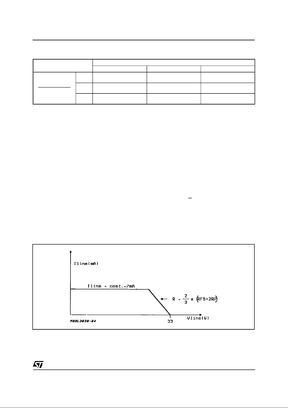
Table 1.
Pin 27 of L3030
of L3000S
Pin
11
Pin 28 of L3030 / Pin 12 of L3000S (C2)
+3 0 –3
+ 3 Stand-by Conversation in Normal
Battery Direct Polarity
0 Not allowed. Conversation in Boost
Battery Direct Polarity
– 3 Not allowed. Ringing with Direct
Polarity
L3000S - L3030
Conversation in Normal
Battery Reverse Polar
Conversation in Boost
Battery Reverse Polar
Not allowed.
statesas listed in Table.1.
Appropriate combinations of two pins define the
threemodesof theST SLIC,thatare :
a) Stand-by(SBY)
b) Conversation(CVS),Normal and Reversepolarity
c)Ringing (RING)
d)Boost Battery(BB),Normaland Reversepolarity
A fifthstatus,Powerdown (PD),can be set disconnectingthebiasresistor(RH)frompin10 ofL3000S
bymeansofanexternal transistor.
The maindifferencebetween Stand-byand Power
downis that in SBY thepower consumptionon the
voltage battery VB– (– 48V) is reduced but the
L3000SDC feedingandmonitoringcircuitsare still
active.In PD the power consumptionon VB- is reducedto zero, and the L3000Sis completelyswitchedoff.
TheSBYstatusshouldbeusedwhenthetelephone
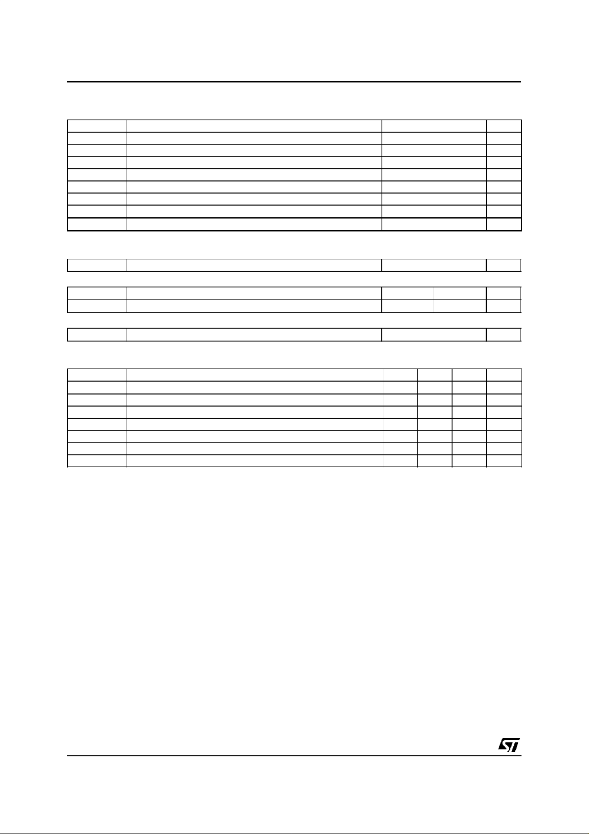
Figure1 : DC Characteristicsin Stand-byMode.
isinOnhookand PDstatusonlyinemergencyconditionwhen it is mandatorytocutany possibledissipationbut no operationare requested.
OPERATINGMODES
Stand-by(SBY) Mode
In thismode,the bias currentsof both L3000S and
L3030arereducedasonlysomepartsofthetwocircuits are completely active, control interface and
currentsensorsamong them.The currentsupplied
tothe lineis limited at7mA,andthe slopeof theDC
characteristiccorrespondsto :
2
R =
(RFS+ 2RP)
x
3
TheLinevoltageinonHookconditionisjustthebatteryvoltageminusthevoltagedrop(approx.15V)of
theoutputstageamplifiers(see Fig. 1).
7/29
L3000S - L3030
The AC characteristic is just the resistance of the
twoserialresistorsRP.
InStand-bymodethebatterypolarityisjustindirect
condition,thatistheTIPwiremorepositivethanthe
RING one ; boost batteryis not achievable.There
are two possiblelineconditionswherethe SLIC is
expectedto be in stand-bymode :
1) ON-HOOK(I
<5mA).Normalon-hook
line
condition.
2) OFF-HOOK (I
> 7mA).Handset is unhooked,
line
the SLIC is waiting for command to activate
conversation.
Whenthe SLICis in stand-bymode,the powerdissipationof L3000Sdoes not exceed120mW(from
-48V) eventually increased of a certain amount if
somecurrent isflowinginto the line.
Thepowerdissipationof L3030in thesamecondi-
tion,is typically120mW.
TheStand-byModeis setwhenthebytesentto the
L3030 Serial Digital Interface has the first two bits
(BIT0Rand BIT1R)equalto ”0”.
Settingto 0 allthe8bitsof thecommandsentto the
digitalinterface of L3030,the bias currentsof both
L3000S and L3030 are reduced and only some
parts of the two circuits are active similarly to the
stand-by mode ; in this situation, named powerdown denial, the line sensors are disabled
(ON/OFF-HOOKlineconditionscannotbe recognized)andthecurrentsuppliedto thelineislimited at
0.25mA.
Conversation(CVS)or ActiveMode
Inconversationmodeitispossibletoselectbetween
twodifferentDCCharacteristicsbytheBIT5Rof the
SerialInterface.
1) NormalBattery(NB)
2) BoostBattery (BB)
Itisalsopossibleto select(BIT4R)thepolarityofthe
DCline voltageand (BIT6R-BIT7R) oneof the four
valuesof limiting current(25mAor 30mAor 45mA
or 70mA).
Batteryreversecan takeplaceeither before or duringconversation.
As farastheDCcharacteristicin Normal Batteryis
concerned, three different feeding conditions are
present:
a) currentlimiting region; theDC impedanceof the
SLICis veryhigh (> 20 Kohm)and thereforethe
systemworkslikeacurrentgenerator,thecurrent
value being set through the digital interface
(25/30/45/70mA).
b) standard feeding system region ; the
characteristicis equal to a – 48V(– 60V)battery
(note1),inserieswithtworesistors,whosevalue
is set by external components (see external
componentlistof L3030).
c) low impedance region ; the battery value is
reducedto 33V(45V)andtheserialresistanceis
reducedtothevaluespecifiedin standby mode,
2
thatis:
x (RFS+ 2RP)
3
Switchingbetweenthethreeregionisautomaticwithout discontinuity, and depends on the loop resistance.Fig.2 showstheDCcharacteristicin normal
batterycondition.
Whentheboostbatteryconditionisactivatedthelow
impedanceregioncan neverbereachedbythe sy-
Figure2 :
Note : 1. Thisvalue ofvoltagebattery, namedapparent battery,is fixedinternally by the control unit and is independent of the actualbattery
8/29
DCCharacteristic(n.b.)I
value.So,thevoltagedropin thelowimpedance regionis 15V.It is alsopossible toincreaseup to25Vthis valuesetting BIT3R to 1.
= 25/30/45/70mA.
LIM
L3000S - L3030
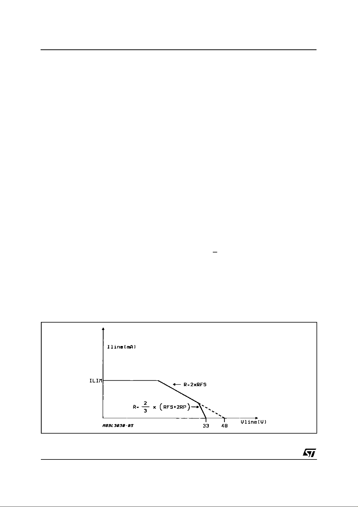
stem ; in this case the internal dropout voltage is
equalto30V.
Fig.3 shows the DC characteristicin boost battery
condition.
Inconversationmode,onrequestofcontrolprocessor,whateverconditionis set(normalor boostbattery, direct or reverse polarity), you can inject the
12kHz(or16kHz)signal(permanentlyappliedatthe
pin33with950mVrmstyp.amplitude),as metering
pulses.A patentedautomaticcontrolsystemadjust
the level of the meteringsignal,acrossthe line, to
2Vrmssetting BIT3= 0, orto5VrmssettingBIT3 =
1 ;this,regardlessof thelineimpedance.Moreover
the meteringsignal is rampedat thebeginningand
atthe endof eachpulseto preventundesirableclickingnoise ; the slopeis determinedby the value of
CINT (see the external component list of L3030).
The SLIC also provides, in the transmit direction
(fromlineto4-wireside),anamplifiertoinsertanexternalnotchfilter(seriesresonator)forsuppressing
the 12/16kHzresidualsignal.
Fig.4 showsasuggestednotchFilterconfiguration.
Themeteringpulses canbeinjectedwith aDC line
currentequal to zero(ON-HOOK Operation).
Ifteletaxisnotusedthe notchfiltercan bereplaced
bya 1KΩ resistor.
Inconver s ationmodetheACimpedanc eatthelineterminals,ZML,issyn thetizedbytheext er nalcomponents
ZACandRP,accor dingto thefollowingform ula:
ZML=ZAC+ (RP1+ RP2)
Dependingon thecharacter i s ticoftheZACnetwork,
ZMLcanbe eitherapureresistanceoracompleximpedance,soallow i ngSTSLICtomeetdifferentstandards as far as the return loss is concerned. The
capacitorCCOMPguaranteesstabilitytothesystem.
Thetwo-to-fourwireconversionis achievedbymeansof aWheatstonebridgeconfiguration,thesides
of whichbeing:
1) the lineimpedance(Zline),
2) the SLICimpedanceatlineterminals(ZML),
3) thenetworkZAconnectedbetweenpin36and41
ofL3030(seeexternalcomponentlist ofL3030),
4) the networkZBbetweenpin 36 and groundthat
shallcopy the line impedance.
Fora perfectbalancing,thefollowingequationshall
beverified :
ZA
ZML
=
ZB
Zline
It is importantto underlinethat ZA and ZB are not
obliged to be equal to ZML and to Zline, but they
bothmay be multipliedby a factor(up to ten)so allowinguse of smallercapacitors.
Inconversation,theL3000Sdissipatesabout250mW
foritsownoperation;thedissipationdependingonthe
currentsuppl i edtothe line shall be added.
Thefig5andfig6showtheDCcharacteristicfortwo
differentFeedingresistance.
2x 200Ohmand 2 x 400respectively.
Figure 3 : DC Characteristic(b.b.)
I
= 25/30/45/70mA.
LIM
Figure4 : ExternalTeletaxeFilter.
1
f
=
LxC
2π
√
R2 x R4 xR5
L
=
R3
xC2
9/29

L3000S - L3030
Figure5 : DCCharacteristicfor2 x 200 ohm FeedingSystem.
Figure6 : DCCharacteristicfor2 x 400ohm FeedingSystem.
Figure7 : LineCurrentVersusLoop Resistance,RFS= 200Ω,R
10/29
=30Ω,VB– =–48V.
P

L3000S - L3030
Ringing Mode
Whenringingisselected(BIT2R=1,BIT0R=0),the
control unit L3030 presets the L3000S to operate
between– 48V (– 60V) and + 72V(+ 60V) battery.
Then,settingBIT1=1,alowlevelsignal(0.285Vrms
withfrequencyrange16-66Hz)appliedtopin41, is
amplifiedandinjectedin balancedmode to the line
throughL3000SwithasuperimposedDCvoltageof
24V.Theimpedancetothe line is given by the two
externalresistorsandthe 24V DC polaritycan only
bedirect.
Thefirstandthelastringingcyclesaresynchronized
byL3030so thatringing alwaysstarts andstopsat
zero crossing. Ring trip detectionis performedautonomouslybytheSLIC,withoutanyparticularcommand, usinga patentedsystem; when handsetis
lifted,SLIC suspendstheringing signal just remainingintheringingmode.Inthiscondition,thecontrol
unitL3030checksthatthe loop is closedfora time
equalto twoperiodsof theringingsignal ; if theclosureis confirmed, a flag(BIT0T = 1) is set and the
SLICwaitsthenewcommandfrom the controlprocessor.Whereasthe loop closureis not confirmed,
theringingsignalisnewlyappliedto theline,without
settingBIT0T.
DIGITAL INTERFACE
FunctionalDescription
The L3030 states and functions are controlled by
centralprocessorthroughfive wiresdefininga digitalinterface.Itispossibleto selecttheinterfaceworkingmodebetween SERIALor PARALLEL(pin33
tiedto a voltagebetween 4 and 5V).
1) SerialMode
Thefivewires of the digitalinterfacehavethe followingfunctions:
- clock(DCLK), enteringat pin 21
- data in/dataout (DIO),exchangedat pin 20
- input/outputselect(EIA), enteringat pin 18
- chip select(NCS),enteringat pin 19
- changeNCS fromin to out (CI),enteringat pin26
(note1)
Themaximum clockfrequencyis 600Khz.
WhenEIAsignalis lowdataaretransferredfromthe
cardcontrollerintoI/O registersoftheL3030selected by NCS signal tied at low level ; then data are
latchedforexecution.In thisphasea complete8bit
wordisloadedintointernalregisterandconsequently NCS signal must remain low for the corresponding 8 clock pulses (DCLK). The EIA signal must
remainatlowlevelatleastforthetimeinwhichNCS
signalremainlow. The deviceload dataininputregister during the positive edge of clock signal
(DCLK)andstore thecontentsoftheregisteronthe
positiveedgeof NCS signal.
When EIA signal is high data are transferred from
the L3030selectedby NCS tied to low level to the
card controller. The L3030 status is described by
five bits containedin the output register; the NCS
signalcanremainlowforfiveor lessclockpulsesdependingif thecardcontrollerwant to read thecompleteL3030 statusor only a partof it.
Fig.8,9showthecompletewriteandreadoperation
timing.Table 1showsthemeaningof eachbitofan
I/Odata.
11/29

L3000S - L3030
Table 1 :
Serial Mode.
Meaning Value
Data in (note 2)
BIT0R = Impedance (note 3) 0 - Stand-by/ringing
1 - Conversation
BIT1R = TTX & Ring Timing (note 4) 0 - Timing off
1 - Timing on
BIT2R = Ring (note 5) 0 - TTX Signal Injection
1 - Ring Signal Injection
BIT3R = TTX Level 0 - Low Amplitude (2V
1 - High Amplitude (5V
RMS
RMS
)
BIT4R = Battery Polarity 0 - Normal Polarity
1 - Reverse Polarity
BIT5R = Extra Feeding 0 - Normal Battery
1 - Boosted Battery
BIT6R
BIT7R
Current
Limiting
0
25mA
0
0
30mA
1
Data Out (note 6)
BIT0T = Line Supervision 0 - On Hook
1 - Off Hook
BIT1T = Ground Key 1 - Long. Line Current < 17mA
0 - Long. Line Current > 17mA
BIT2T = Internal Line Current Limiter (note7) 0 - Off
1-On
BIT3T = Line Voltage 0 - Normal
1 - Minus of Half Battery
BIT4T = Thermal Overload (note 8) 1 - Off
0-On
)
1
45mA
1
1
70mA
0
Notes : 1. When C I signal is tied to low level, NCS signal is t he chip sele ct input ; w ith C I si gnal at high l e v e l, the NCS si gna l
becomes an output that carry out the l ogical sum of the f ol lowing bi t s : BIT0T, BIT1T.
2. The desc r i ption of t he commands i s referred to the s ys t em L3030 + LIN E INTER FACE mod ule.
3. To set SBY mode wi th I
4. TT X and R I N G signals are i njected into the li ne in t er face modul e with BIT 1R to ”1”.
5. To s et RING mode at least one of t he three last bits (BIT5R, B I T6R, BIT7R) must be set to 1, in addi tion BIT0R
must be set to 0.
6. The desc r i ption of t he commands i s referred to the s ys t em L3030 + LIN E INTER FACE mod ule.
7. The bit BIT2T is set to 1 w hen the SLIC is operating in Conversation Mode and int o the li m iting current region (shor t
loop).
8. The bit BIT4T is set to 1 when t he j unctio n tem perature of L3000S is a bout 140°C.
= 7mA : B I T0R = 0 and at least o ne of the two l ast bits (BIT6R ; BI T7R) must be set t o 1.
lim
12/29

Figure8 : WritingOperationTiming(serialmode).
L3000S - L3030
Figure9 : ReadingOperationTiming(serialmode).
13/29

L3000S - L3030
2) ParallelMode
In thisoperatingmodethe signalsat the inputsare
immediatelyexecuted,withoutanyexternalclocktiThis operatingmode is enabled connectingpin 33
toa voltageintherangefrom4Vto5V.Thefivewire
havethe followingfunctions:
- power down/feeding(EIA),enteringat pin 18
- timing (CI),enteringat pin 26
- ring (DCLK), enteringat pin21
- on-hook/off-hook(NCS), outgoingat pin19
- ground-key(DIO),outgoingat pin20
ming;alltheinternalregistersarebypassed.Thein-
formationssent backon pins19 and 20, display in
realtime thesettingof internalcircuits, that means
line status. In the table 2 the correspondencebet-
ween the interface wires in the parallel mode and
equivalentbit in serial mode is pointedout; where
thereisn’tthis correspondence,the internalsetting
isshown.
Table 2 : Parallel Mode.
Pin Rif. Meaning (note 1) Eq. Bit of Ser. Interf. Value
18 EIA PD/feeding BIT0R 0 : High Impedance
1 : Low Impedance
26 CI Timing BIT1R 0 : Ring Timing Off
1 : Ring Timing On
21 DCKL Ring BIT2R 0 : No Ring
1 : Ring Injection
BIT3R 0 : Low Amplitude
BIT4R 0 : Normal Polarity
BIT5R 0 : Normal Battery
BIT6R 0 :
BIT7R
19 NCS On-hook/off-hook BIT0T 0 : On-hook
20 DIO Ground Key BIT1T 1 : Long. Curr. < 17mA
BIT2T
BIT3T
BIT4T
Line Curr. = 30mA
1:
1 : Off-hook
0 : Long. Curr. > 17mA
Note : 1. Thedescription of the commandsis referredto the system L3030+ LINE INTERFACE module.
DIGITAL INTERFACE ELECTRICAL CHARACTERISTICS
=+5V,VSS= – 5V, T
(V
DD
Symbol Parameter Test Conditions Min. Typ. Max. Unit
STATIC ELECTRICAL CHARACTERISTICS
Vil Input Voltage at Logical ”0” Pins 18, 19, 20, 21, 26 0 0.8 V
Vih Input Voltage at Logical ”1” 2.0 5 V
Iil Input Current at Logical ”0” Vil = 0V 200
Iih Input Current at Logical ”1” Vih = 5V 10
Vol Output Voltage at Logical ”0” Pins 19, 20 Iout = – 1mA 0.4 V
Voh Output Voltage at Logical ”1” Pins 19, 20 Iout = 1mA 2.4 V
Ilk Tristate Leak. Current Pin 20 NCS = ”1” 10 µ
14/29
.=25oC) (refer to PLCC44 package)
amb
A
µ
A
µ
A

L3000S - L3030
DIGITAL INTERFACE ELECTRICAL CHARACTERISTICS (continued)
Symbol Parameter Test Conditions Min. Typ. Max. Unit
DYNAMIC ELECTRICAL CHARACTERISTICS
fclk Clock Frequency 1 600 kHz
Tr, Tf Clock Rise and Fall Time 50 ns
Twh, Twl Clock Impulse Width 750 ns
Tis CI to NCS Set up Time 300 ns
Tec ”0” EIA to DCKL Set up Time 300 ns
Tsc DCKL to NCS Delay (+ edge) 300 ns
Tsd Data in Set up Time 0 ns
Thd Data in Hold Time 800 ns
Tcs NCS to DCKL Hold Time 800 ns
Tca ”0” EIA to DCKL Hold Time 900 ns
Tac ”1” EIA to DCKL Set up Time 400 ns
Tzd Data out to ”0” NCS Delay 0 600 ns
Tce ”1” EIA to DCKL Hold Time 900 ns
Tdz Data out to ”1” NCS Delay 500 ns
Tdd Data out to DCKL Delay 1500 ns
Tsi ”0” CI to NCS Hold Time 300 ns
OPERATIONDESCRIPTION
To set SLIC in operation the following parameters
haveto be defined:
- the DCfeedingresistanceRFS, definedasthe resistanceofeachsideof the traditionalfeedingsystem (most common valuesare 200, 400 or 500
ohm).
- theACimpedanceat lineterminals,ZML, towhich
thereturnlossmeasurementreferences.Itcanbe
real(typically600 ohm)or complex.
- the equivalent AC impedance of the line Zline,
when evaluating the trans hybrid loss (2/4 wire
conversion).Itisusuallya compleximpedance.
- the ringing signal frequency Fr (ST SLIC allows
frequencyrangingfrom16 to 66Hz).
- the metering pulse frequencyFt (two values are
possible: 12kHzor 16kHz).
- the value of the two resistors RP1/RP2 in series
with the line terminals; main purposeof the a.m.
resistors is to allow primary protectionto fire. ST
suggest the minimum value of 50 ohm for each
side.
Onthisassumptions,the following componentlistis
defined.
15/29

L3000S - L3030
EXTERNAL COMPONENT LIST FOR THE LINE INTERFACE
Pin
Ref. Value
L3000S
10 RREF
1,15 RP
7 CDVB
3 CVB+
8 CVB–
8 D1 BAT 49X Protective Shottky Diode
L3030 (PLCC44)
4-3 CVSS
5-3 CVDD
7-8 RR
15-17 RDC 2 x (RFS – RP1)
7-15
CAC1 (3)
14-15 CAC2 CAC1
8-9 ZAC ZML – (RP1 + RP2) 2 Wire AC impedance
8-9 CCOMP 1/(6.28 x 150000 x (RPC)) AC loop compensation
9-14 RPC RP1 + RP2 Rp insertion loss compensation
2-3 RREF
36-3 ZB K x Zline (note 4) Line Impedance Balancing Network
36-41 ZL K x RPC in Series with
32-3 CINT (note 6) Ring trip detection time constant
15-16 Ccon
35 TTx FILT.
34 R
GTTX
Component
24.9k
Ω ±
30 to 100
47µF – 20V
0.1µF – 100V (1)
0.1µF – 100V (2)
0.1µF – 15V
0.1µF – 15V
16K
(range: 10 to 50K
Ω
1
6.28
x 250 x (ZAC+ RDC)
24.9KΩ1%
K x ZAC // (CCOMP/K)
0.15µF (note 7)
=1kΩ1% in speech band
Z
TTX
Z
TTX
at TTX freq. (note 9)
≈0Ω
10kΩ 1%
1%
Ω
Ω)
Involved Parameter or Function
Bias Resistance
Line Series Resistor
Battery Voltage Rejection
Positive Battery Filter
Negative Battery Filter
Negative Supply Voltage Filter
Positive Supply Voltage Filter
Capacitor Multiplier Gain (8)
DC Feeding Resistor (RDC > 270Ω)
AC Path decoupling
Bias Resistance
SLIC Impedance Balancing Network (note 5)
Interface Time Constant
Teletax filter.
Teletax filter.
Notes :
1. In cas e line cards wi th les s than 7 subsc r ibers ar e implem ented CVB – capacitor shoul d be eq ual to 680 nF/N w here
N i s the num ber of subscr iber per car d.
2. T hi s shottky diode o r equi valent is necessary t o avoid to damage to the device dur ing h ot ins e r tion or i n al l thos e
cases when a proper power up sequenc e canno t be guaran te ed.
In case t he shott k y diode i s not implemented the power sequenc e should guarant ee that VB+ is always the las t
supply applied at power on and the first remove d at pow er off.
In case an other shottky diode t ype i s adopted it must ful fil l the f ol lowi ng charac t eristics:
< 450mV @ IF=n⋅15mA, T
V
F
V
< 350mV @ IF=n⋅15mA, T
F
< 245mV @ IF=n⋅15mA, T
V
F
Where n is t he number of li ne sharing the sam e diode.
3. If t he in t er nal ca pacity mul t i plier stage i s not used, pin 7 must be c o nnec ted w i th pin 14 w i thout mounti ng RR and
CAC2. In this case CA C1 = 1/(6.28 x 30 x RD C).
4. The structure of this network shall copy the line impedance, in case multiplied by a factor K = 1....10
5. K as fi xed at note 4.
6. CINT can h av e the follow ing v al ues :
=25°C
amb
=50°C(T
amb
=85°C(T
amb
jL300 0
jL300 0
=90°C)
= 120 °C)
Fr. (Hz) 16/18 18/21 21/26 26/31 31/38 38/46 46/57 57/66
CINT (nF) 560 470 390 330 270 220 180 150
7. Cc on is necessary to w or k ”without on/off hook det ect ion-err ors” during T T X - pulses.
8. RR i s used by a capacitor mult i plier circuit to s ynthetize an higher AC / D C splitting capaci tor st ar ting fr om CAC1
and CA C2. S upposing CAC1 = CAC 2 = C AC the syntheti zed capacitor val ue wil l be eq ual
9. If Te letax is not us ed the T TX FILT . can be r epl aced by a 1kΩ resistor .
RR + ZML
ZML
16/29
⋅ CA C.

Figure10 : TypicalApplicationSchematicDiagram.
L3000S - L3030
L3000S
Figure11 : TypicalApplicationSchematicDiagramwithoutCapacitorMultiplier.
L3000S
17/29

L3000S - L3030
ELECTRICAL CHARACTERISTICS (refer to the test circuits of the Figure 12, VDD= + 5V, VSS=-
5V, V
+=+72V,VB– = – 48V, T
B
Symbol Parameter Test Conditions Min. Typ. Max. Unit
STAND-BY
Vls Output Voltage at L3000S
Terminals
Ilcc Short Circuit Current DATA IN (note 1) 000X00X1 5 8.5 mA
Iot On/off-hook Detection Threshold 5 8.5 mA
Vls Symmetry to Ground Iline = 0mA .75 V
STAND BY DENIAL
Ilcc Short Circuit Current DATA IN 000X00X0 2 mA
DC OPERATION - NORMAL BATTERY (V
Vlo Output Voltage at L3000S
Terminals Ilim = 70mA Data in
1000X010
Ilim Current Programmed Through
the Digital Inter.
Io On-hook Detection Threshold 8 mA
If Off-hook Detection Threshold 12 mA
Ilgk Longitudinal Line Current with
GK Detect
DC OPERATION - BOOST BATTERY
Vlo Output Voltage at L3000S
Terminals
AC OPERATION
Ztx Sending Output Impedance
4 Wire Side
Zrx Receiving Input Impedance
4 Wire Side
THD Signal Distorsion at 2W and 4W
Terminals
R1 2W Return Loss f = 300 to 3400Hz 22 dB
Thl Trans Hybrid Loss f = 300 to 3400Hz 24 dB
Gs Sending Gain Vso = 0dBm f = 1020Hz
Gsf Sending Gain Flatness versus
Frequency
Gsl Sending Gain Linearity fr = 1020Hz,
Gr Receiving Gain Vri = 0dBm f = 1020Hz
Grf Receiving Gain Flatness f = 300 to 3400Hz Respect
=+25oC, TTX FILT = 1kΩ)
amb
Iline = 0mA
Iline = 5mA
=2VRMS, low level)
TTX
Iline = 0mA
Iline = 20mA
Iline = 50mA
Iline = 0mA
Iline = 20mA
Norm. Polarity – 0.25 + 0.25
f = 300 to 3400Hz Respect
to 1020Hz
Vsoref = –10dBm
Vso = + 4 /– 40dBm
Norm. Polarity – 0.25 0 + 0.25
to 1020
30.0
28.2
31.0
24.0
2.5
40.0
38.5
35.0
28.8
17.5
– 10% Ilim + 15% mA
10 17 26 mA
86
68.6
95.6
81
10 Ω
100
0.5 %
– 0.1 + 0.1 dB
– 0.1 + 0.1 dB
– 0.1 + 0.1 dB
k
dB
dB
V
V
V
V
V
V
V
Ω
Notes : 1. The dat a into the di gital int er f ace of L3030 are send in serial mode. The for m at of data i s the following :
a) DATA IN : t he bi t at left si de i s BI T 0 of t he wr iting word, whi le the bit at the right side is BIT 7.
b) DATA OUT : the bi t at the lef t si de is BIT0 of the rea din g wor d, while the bit at the right i s BIT4.
When appear a sym bol X, the value of the bit don’t ca r e.
18/29

L3000S - L3030
ELECTRICAL CHARACTERISTICS (continued)
Symbol Parameter Test Conditions Min. Typ. Max. Unit
AC OPERATION (continued)
Grl Receiving Gain Linearity fr = 1020Hz, Vriref = – 10dBm
Vri = + 4 /– 40dBm
Np4W Psophometric Noise at 4W-Tx
Terminals
Np2W Psophometric Noise at Line Terminals – 75 – 70 dBmp
SVRR Supply Voltage Rejection Ratio
f = 3400Hz – 30 dB
Relative to VB–
SVRR Relative to V
SVRR Relative to V
DD
SS
f = 3400Hz
Vs = 100mVrms
Ltc Longitudinal to Transversal Conversion f = 300 to 3400Hz
Tlc Transversal to Longitudinal Conversion 48 51 dB
Iline = 30mA, ZML = 600
Td Propagation Time Both Direction 40
Tdd Propag. Time Distortion 25
Vttx Line Voltage of Teletaxe Signal V
THD Teletaxe Signal Harmonic
= 950mVrms Note 2
TTXin
Note 3
Dist. ttx Filt = 0Ω@ 16kHz
Note 4
Zitt Teletaxe Amplif. Input Impedance Pin 33 of L3030 100
AC OPERATION BOOST BATTERY
Gs Sending Gain Vso = 0dBm f = 1020Hz
Norm. Polarity – 0.66 – 0.16 + 0.34 dB
Gr Receiving Gain Vri = 0dBm f = 1020Hz
Norm. Polarity – 0.27 + 0.08 + 0.43 dB
Np4W Psophometric Noise at 4W-Tx
Terminals
Np2W Psophometric Noise at line Terminals – 73 – 68 dB
SVRR Relative to Vdd f = 3400Hz
Vs = 100mVrms
SVRR Relative to Vss –23 dB
RINGING PHASE
Vlr Superimposed DC Voltage
Vacr Ringing Signal at Line Termin.
Rloop > 100k
Rloop = 1k
Ω
Ω
Rloop = 1kΩ/1µF
If DC Off-hook Det. Threshold 1.5 3.5 mA
Ilim Current Limit. 85 130 mA
Vrs Ringing Simmetry 2 Vrms
THDr Ringing Signal Distortion V
f
RING
AC
= 0.285V
= 30Hz
RMS
– 0.1 + 0.1 dB
– 75 – 70 dBmp
– 30 – 26 dB
– 32 – 30 dB
49 (1) 60 dB
Ω
1.7
4.5
– 73 – 68 dBmp
19
17
23
21
56 Vrms
2.3
5.5
5%
–23 dB
27
25
5%
µ
µ
V
V
kΩ
V
V
s
s
Notes : 1. U p t o 52dB us i ng sel ect ed L3000 S.
2. The configuration of dat a sen t to devi c e c hange, eve r y 100 m S , from - 1100X 010 - t o - 1000X 010 -
3. The configuration of dat a sen t to devi c e c hange, eve r y 100 m S , from - 1101X 010 - t o - 1001X 010 -
4. Err or gener at ed by ttx fi lt≠0 ohm , on the output t eletax amplit ude i s err% = 100 x (1 + A) x B /C where A = 10
Kohm /RGTTX[Kohm], B = TTX FILT[ Kohm], C = (TTXF IL T [Kohm] + 1 Kohm) , f or exampl e 10 oh m means er r % = 2%.
19/29

L3000S - L3030
ELECTRICAL CHARACTERISTICS
Symbol Parameter Test Conditions Min. Typ. Max. Unit
RINGING PHASE
Zir Ringing Amplif. Input Impedance Pin 41 of L3030 100
Vrr Residual of Ringing Signal at TX
Trt Ring Trip Detection Time
Toh Off-hook Status Delay after the
Trs Cut off of Ringing Ring Trip not Confirmed 188
SUPPLY CURRENT
IDD Positive Supply Current CS = 1 Stand-by
ISS Negative Supply Current CS = 1 Stand-by
I
BAT–
I
BAT+
Output
Ringing Stop
Negative Battery Supply Current Line
Current = 0mA
Positive Battery Supply Current Line
Current = 0mA
(continued)
fring = 16Hz
T = 1/fring
Conversation (NB/BB)
Ringing
Conversation (NB/BB)
Ringing
Stand-by
Conversation NB
Conversation BB
Ringing
Stand by
Conversation NB
Conversation BB
Ringing
(1T)
16.0
26.0
16.5
9
19
9
2
5
6.6
14
10
10
8
12
600 mV
125
(2T)
125
(2T)
(3T)
20.0
31.0
21.0
12
23
12
2.5
6.5
8.0
17
15
15
10
13.5
kΩ
ms
ms
ms
mA
mA
mA
mA
mA
mA
mA
mA
mA
mA
µA
µ
mA
mA
A
NB = Normal Battery
BB = B oosted Bat t er y
Figure12 :
SlicTest CircuitSchematic.
L3000S
20/29

Figure 13: Typicalapplicationschematic with 2ndgenerationCOMBO.
VB+
BGND
4
30Ω
3
1
L3121
22nF
2
22nF
4
2
3
L3121
1
L3000S - L3030
BGND
VB+
ZBZA
CVB+
BGND VB+
RL CVSS
TTXIN TX AGND
CVB-
REF
CINT
VB-
20Ω
D1
VB-
8
43
VSS
VSS
4
2
33 40 3
32
36
CRTS
L3000N
L3000S
VDD
CVDD
41
ZB
RX
TIP
5
VDD
VDD
5
CZS7ACF
(*)
CTL
1
9
AGND
TTX
TTXF35
8
CCOMP
MNT
RH
FILTER
L3030
9
REF
CDVB
RGTTX
RGTTX
ZAC
ZAC
VB-
20Ω 30Ω
RING
2
107614121113
IL
IT
C2
C1
VIN
VBIM
14
13
CM
CAC1
C127C228IL31VOUT
IT
15RC17
RDC
34
VBIM
42
RPC
15
D94TL126
CON
C
16
26
CI
20 21
DIO DCLK
EIA NCS
TO/FROM CARD CONTROLLER
is provided bythe CODEC.
RMS
= 285mV
RING
18 19
RDC
+5V-5V
100nF
100nF100nF
VFRO
2
28
CC
V
GNDV
1819202122168109
SS
DX0
DX1
TSX0
TSX1
VRING=
285mVrms
IL0
TS5070
Fsx
BCLK
26
FSR
IL1
25
DR0
IL2
7
DR1
IL3
IL4
IL5
MR
6
242315
1413111217
CI
CS
CO
CCLK
(*) The analog multiplexer can be avoided if the V
MCLK
21/29

L3000S - L3030
Figure 14: Typicalapplicationschematic with 1stgenerationCOMBO.
VB+
BGND
22nF
22nF
4
2
3
L3121
1
VB-
VB-
4
30Ω
3
2
L3121
1
+5V-5V
BGND
R3
100nF100nF
CVB-
CVB+
VB+
43
BGND VB+
RL CVSS
REF
33 40 3
TTXIN TX AGND
ZBZA
CINT
C
R4
VFXI-
CC
V
GNDAV
VB-
2
32
GSX
8
VSS
VSS
4
36
CRTS
(*)
R1
L3000N
L3000S
VDD
CVDD
41
ZB
RX
VFRO
D1
(**)
R2
20Ω
TIP
1
5
VDD
AGND
TTXF35
VDD
5
8
CZS7ACF
VRING=
ETC5057
MNT
107614121113
9
REF
RH
CDVB
TTX
RGTTX
FILTER
RGTTX
34
L3030
9CM14
ZAC
ZAC
CCOMP
CTL
(FROM
285mVrms
VBIM
VBIM
42
RPC
CARD
2
IL
VIN
13
CAC1
CONTR.)
20Ω 30Ω
RING
IT
C2
C1
IT
C127C228IL31VOUT
15RC17
RDC
15
16
26
20 21
18 19
RDC
VFXI+
C
CON
CI
DIO DCLK
EIA NCS
D94TL127A
TO/FROM CARD CONTROLLER
(*) Resistors R1 to R4 program IX/RX gains ZA, ZB shold be >>than R2.
is provided by the CODEC.
RMS
= 285mV
RING
(**) The analog multiplexer can be avoided if the V
22/29
SS
DX
DR
TSX
MCLKX
MCLKR/
BCLK
BCLKR/
FSR
FSX

L3000S - L3030
APPENDIX
SLIC TEST CIRCUITS
Referring to the test circuitreportedatthe endof eachSLICdatasheetherebelowyou can find the proper
configurationfor eachmeasurement.
In particular: A-B: Lineterminals
C : TX sendingoutputon 4W side
D : RX receivinginput on 4W side
E : TTX teletaxesignal input
R
: lowlevelringingsignalinput.
GIN
TEST C I RCUITS
Figure1 : Symmetryto Ground.
Figure3: Trans-hybridLoss.
Figure2 : 2WReturnLoss.
R
WC
1
L
=
<<Z
20 log
− Z|
L
|Z
+ Z|
L
|2 V
log
S
|E|
20
=
|Z
Figure4: SendingGain.
|
THL
20log
=
|VS|
10
|VR|
GS= 20 log
|VR|
10
|V
|
SO
23/29

L3000S - L3030
TEST CI R CUITS (continued)
Figure5 : ReceivingGain.
GR= 20 log
Figure7 :
| VR|
10
| VS|
Longitudinalto TransversalConversion.
Figure6 : SVRRRelativetoBatteryVoltageVB–.
V
|
|
SVRR=20 log
Figure8 :
n
|
V
|
R
Transversalto LongitudinalConversion.
L
= 20 log
T
Figure9 :
|
|V
R
|E
|
TTXLevelat Line Terminals.
T
= 20 log
L
10
Figure10 :
| VR|
|V
|
S
RingingSimmetry.
24/29

PLCC44 PACKAGE MECHANICAL DATA
L3000S - L3030
DIM.
MIN. TYP. MAX. MIN. TYP. MAX.
A 17.4 17.65 0.685 0.695
B 16.51 16.65 0.650 0.656
C 3.65 3.7 0.144 0.146
D 4.2 4.57 0.165 0.180
d1 2.59 2.74 0.102 0.108
d2 0.68 0.027
E 14.99 16 0.590 0.630
e 1.27 0.050
e3 12.7 0.500
F 0.46 0.018
F1 0.71 0.028
G 0.101 0.004
M 1.16 0.046
M1 1.14 0.045
mm inch
25/29

L3000S - L3030
FLEXIWATT 15 PACKAGE MECHANICAL DATA
DIM.
A 5.00 0.196
B 1.90 0.074
b1 0.1 0.004
D
E 0.30 0.012
F 0.90 0.035
F1 0.57 0.022
G 1.77 1.9 2.03 0.070 0.075 0.080
G1 26.77 1.054
H1 29.00 1.142
H2 28.00 1.102
H3 17.00 0.669
H4 0.80 0.031
L 19.05 19.95 0.75 0.785
L1 1.10 1.40 0.043 0.055
L2 2.60 2.90 0.102 0.114
L3 15.35 15.65 0.604 0.616
N1 10 0.394
N3 6.8 0.268
N4 3.8 0.15
Dia1 13.00 0.511
MIN. TYP. MAX. MIN. TYP. MAX.
mm inch
4°(typ.)
N1
N4
G
H1
H2
H3
Dia.2
Dia.4
H4
b1
A
Dia.1
N3
L3
L
L1
E
B
G1
Dia.3
F
F1
L2
D
FLEX15
D
26/29

PowerSO-20(slug-up) PACKAGE MECHANICAL DATA
L3000S - L3030
DIM.
mm inch
MIN. TYP. MAX. MIN. TYP. MAX.
A 3.70 0.145
a1 0 0.25 0 0.01
b 0.40 0.53 0.016 0.021
c 0.23 0.32 0.009 0.012
D 15.80 16.00 0.622 0.63
D1 9.4 9.80 0.37 0.385
E 13.90 14.50 0.547 0.57
e 1.27 0.05
e3 11.43 0.45
E1 10.90 11.10 0.429 0.437
E2 2.90 0.114
E3 5.80 6.20 0.228 0.244
G 0 0.10 0 0.004
h 1.10 0.043
L 0.80 1.10 0.031 0.043
N
S
10°(Max.)
8°(Max.)
E2
NN
b
e3
hx45°
20 11
D1(slug width)
D
E3 (slug width)
A
e
101
E1
DETAILA
PSO20DME
Gage Plane
DETAILA
0.35
S
a1
E
L
c
-C-
SEATINGPLANE
GC
(COPLANARITY)
27/29

L3000S - L3030
PowerSO20(slug-down) PACKAGE MECHANICAL DATA
DIM.
mm inch
MIN. TYP. MAX. MIN. TYP. MAX.
A 3.60 0.1417
a1 0.10 0.30 0.0039 0.0118
a2 3.30 0.1299
a3 0 0.10 0 0.0039
b 0.40 0.53 0.0157 0.0209
c 0.23 0.32 0.009 0.0126
D (1) 15.80 16.00 0.6220 0.6299
E 13.90 14.50 0.5472 0.570
e 1.27 0.050
e3 11.43 0.450
E1 (1) 10.90 11.10 0.4291 0.437
E2 2.90 0.1141
G 0 0.10 0 0.0039
h 1.10
L 0.80 1.10 0.0314 0.0433
N
S
10°(max.)
8°(max.)
T 10.0 0.3937
(1) ”D and E1” do not include mold flash or protrusions
- Mold flash or protrusions shall not exceed 0.15mm (0.006”)
NN
b
DETAILA
e3
D
E2
T
110
R
a2
A
e
DETAILB
lead
1120
a1
E
DETAILA
a3
c
slug
DETAILB
E1
Gage Plane
0.35
-C-
S
L
SEATING PLANE
GC
(COPLANARITY)
28/29
hx45°
PSO20MEC

L3000S - L3030
Information furnished is believed to be accurate and reliable. However, SGS-THOMSON Microelectronics assumes no responsibility for
the consequences of use of such information nor for any infringement of patents or other rights of third parties which may result from its
use. No license is granted by implication or otherwise under any patent or patent rights of SGS-THOMSON Microelectronics. Specifications mentioned in this publication are subject to change without notice. This publication supersedes and replaces all information previously supplied. SGS-THOMSON Microelectronics products are not authorized for use as critical components in life support devices or
systems without express writtenapproval of SGS-THOMSONMicroelectronics.
1997 SGS-THOMSON Microelectronics – Printed in Italy – All Rights Reserved
PowerSO-20 is a Trademark of the SGS-THOMSON Microelectronics
Australia - Brazil - Canada - China - France - Germany - Hong Kong - Italy - Japan - Korea - Malaysia - Malta - Morocco -
The Netherlands - Singapore - Spain - Sweden - Switzerland - Taiwan - Thailand - United Kingdom - U.S.A.
SGS-THOMSON Microelectronics GROUP OF COMPANIES
29/29
 Loading...