

IMAGE AN D SI G NAL PROCESSING SUB– SYS TE M
SUNSTAR传感与控制 http://www.sensor-ic.com/ TEL:0755-83376549 FAX:0755-83376182 E-MAIL:szss20@163.com
SUNSTAR自动化 http://www.sensor-ic.com/ TEL: 0755-83376489 FAX:0755-83376182 E-MAIL:szss20@163.com
.
1-D/2 -D SOFTWARE CONFIGURABL E C ONVOLVER/FILTER
.
ON-CHIP PROGRAMMABLE LINE DELA YS (0
— 1120 S TAGES)
.
8-BIT DATA AND 8.5-BIT COEFFICIENT
SLICE
.
21 MULTIPLY-AND-A CCUMULATE STAGES
.
1-D (21) OR 2-D (3 x 7) CONVOL UTION WINDOW
.
ON-CHIP POST PROCESSOR FOR DATA
TRANSFORMATION
.
FULLY CASCADABLE IN WINDOW SIZE AND
ACCURACY
.
20 MHZ DATA THROUGHPUT (420 MOP S)
.
SIGNED/UNSIGNED DATA AND COEFFICIENTS
.
MICROPROCESSOR INTERFACE
.
HIGH SPEED CMOS IMPLEMENTA TION
.
TTL COMPATIBLE
.
SINGLE +5V ± 10% SUPPLY
.
POWER DISSIPATION < 2.0 WAT TS
.
100 PIN CERAMIC PGA
IMSA110
PGA100
(Ceramic Grid Array Package)
APPLICATIONS
.
1-D and 2-D digital convolution and correlation
.
Real time image processing and enhancement
.
Edge and feature detect ion
.
Data transformation and histogram equalisation
.
Computer vision and robotics
.
Template matching
.
Pulse compression
.
1-D or 2-D interpolation
July 1992
ORDERING INFORMATION
Part Number Package
IMSA110-G20S PGA100 20MHz commercial
Clock
Speed
Military/
commercial
A110-01.TBL
1/26

IMSA110
SUNSTAR传感与控制 http://www.sensor-ic.com/ TEL:0755-83376549 FAX:0755-83376182 E-MAIL:szss20@163.com
SUNSTAR自动化 http://www.sensor-ic.com/ TEL: 0755-83376489 FAX:0755-83376182 E-MAIL:szss20@163.com
PIN CO NNECTIONS
Index
12345678910
PSRIN
A
B
C
D
E
F
G
H
[6]
CIN
[3]
CIN
[4]
Vcc GND
CIN
[8]
CIN
[9]
CIN
[13]
CIN
[14]
PSRIN
[4]
CLK
CIN
[2]
CIN
[6]
CIN
[10]
CIN
[15]
CIN
[19]
PSRIN
[2]
PSRIN
[7]
CIN
[0]
CIN
[5]
CIN
[7]
CIN
[11]
CIN
[17]
CIN
[21]
[1]
[3]
[5]
CIN
[1]
CIN
[12]
[2]
PSROUT
PSROUT
GND
PSRIN
Vcc
ADR
ADR
PSRIN
PSRIN
PSRIN
GND GND
GND
ADR
[1]
[0]
[0]
[5]
[7]
PSROUT
GND
PSROUT
PSROUT
COUT
GND GND
PSROUT
[2]
PSROUT
PSROUT
[3]
[4]
[5]
D[6]
E2
[5]
[6]
[7]
COUT
[3]
COUT
[11]
COUT
[16]
GND
COUT
[0]
COUT
[2]
COUT
[4]
Vcc
COUT
[12]
Vcc GND
COUT
[19]
Vcc Vcc
COUT
GND
COUT
COUT
COUT
[1]
Vcc
[8]
[13]
[18]
COUT
[6]
COUT
[7]
COUT
[9]
COUT
[10]
COUT
[14]
COUT
[15]
COUT
[17]
COUT
[20]
CIN
J
[16]
CIN
K
[18]
Notes : 1. All VCC pins must be connected to the 5 Volt power supply .
2. All GND pins must be connected to ground.
CIN
[20]
ADR
[0]
RESET
ADR
[1]
ADR
[3]
ADR
[4]
ADR
ADR
1. INTRODUCTION
The IMSA110 is a single-chip reconfigurab le and
cascadable subsystem suitable for many high
speed image and signal processing applications.
Apart from its powerful multiply-accumu late capability (420 MOPs), the strength of the IMSA 1 10 lies
in its extensive programmable support for data
conditioning and transform ation.
2/26
[6]
[8]
E1
W
D[2]
D[0]
D[5] D[7]
D[3] D[4]D[1]
2. DESCRIPTION
The IMSA110 consists of a configurable array of
multiply-accumul ators, three programm able length
1 120 stage shif t registers, a v ersatile post -processing unit and a microprocessor interf ace for config uration and control purposes. The comprehensive
on-chip facilities make a single device capable of
dealing with many image processing operations.
COUT
[21]
A110-01.EPS
Figure 1 : IMSA110 Users Model
SUNSTAR传感与控制 http://www.sensor-ic.com/ TEL:0755-83376549 FAX:0755-83376182 E-MAIL:szss20@163.com
SUNSTAR自动化 http://www.sensor-ic.com/ TEL: 0755-83376489 FAX:0755-83376182 E-MAIL:szss20@163.com
IMSA110
ENABLE 1
ENABLE 2
WRITE
MEM
DATA
ADDRESS
PSRIN
PSROUT
CASCADE
INPUT
Asynchronous Functions
8
Decode
logic
9
8
D
8
22
Synchronous Functions
21 x 8-bit
Update coefficient registers
21 x 8-bit
Current coefficient registers
1120 stage Programmable
shift register (PSRC)
1120 stage Programmable
shift register (PSRB)
1120 stage Programmable
shift register (PSRA)
The IMSA110 has five interfaces through which
data can be transferred, Figure 1. The microprocessor interface allows access to the coefficient
registers, the configuration and status registers,
and the data transformation tables. The remaining
four interfaces allow high speed data input and
output to the IMSA1 10 and the cascading of several
devices. A typical IMSA110 system is shown in
Figure 3. If N devices are used in the cascade, t hey
can be configured, entirely under soft ware c ontr ol,
as a 21N stage 1-D transversal filter or as a 7X by
3Y 2-D window, where X and Y are any integers
satisfying N ≤ XY. For example 4 cascaded devices
can be software configured as: an 84-stage 1-D
filter , a 7 by 12 2-D window, a 28 by 3 2-D window,
or a 14 by 6 2-D window.
The final output of the chip is 22 bits wide in twos
complement format.
Configuration and
Backend
look up table
256 x 8-bit data
transformation
look up RAM
USR LSR
7-stage
multiply-accumulate
array C
7-stage
multiply-accumulate
array B
7-stage
multiply-accumulate
array A
22
control registers
PCR0
PCR1
PCR2
SCR
ACR
post-processing unit
(normalization, saturation,
and data transformation)
BCR
MMB
OUB
TCR
Control
logic
Backend
22
CLOCK
RESET
CASCADE
OUTPUT
Figure 2 shows the distribut ion of the delay s inside
the part.
The latency between P SRin and COUT is dependent upon the length of PSRc. For example, with
PSRc set to 0, and all coefficients set to zero except
CR0c[6] (so the data passes through all MAC
stages), the COUT bus will correspond to the
PSRin bus delayed by 47 clock cycles.
The latency between PSRin and PSRout is 5 cycles
PLUS the lengths of PSRc, PS Rb and PSRa. If t he
shift register s are bypass ed by s etting S CR[ 1] to 1
then PSRout will be PSRin delayed by 2 clock
cycles.
The Latency between the cascade input (CIN) and
cascade output (COUT) is 6 cycles. This is shown
lumped at the cascade input and cascade output
pads in Figure 2. Figure 4 gives details of the data
pipelining through the backend datapath.
A110-02.EPS
3/26
IMSA110
SUNSTAR传感与控制 http://www.sensor-ic.com/ TEL:0755-83376549 FAX:0755-83376182 E-MAIL:szss20@163.com
SUNSTAR自动化 http://www.sensor-ic.com/ TEL: 0755-83376489 FAX:0755-83376182 E-MAIL:szss20@163.com
Figure 2 : Synchronous Functions of the IMSA110
PSRIN
D1
Programmable PSRC
shift register
0 to 1120 stages
8
Programmable PSRB
shift register
0 to 1120 stages
CR1c coefficient registers 7 x 8 bits
CR0c coefficient registers 7 x 8 bits
DD
1
1
2
D
3
X
X
XX
1111
D
8
22
DD D
D
CR1b coefficient registers 7 x 8 bits
CR0b coefficient registers 7 x 8 bits
D
D
1
1
2
D
3
X
X
XX
1111
D
8
22
DD D
D
MUX
D1
PSROUT
Programmable PSRA
shift register
0 to 1120 stages
8
CR1a coefficient registers 7 x 8 bits
CR0a coefficient registers 7 x 8 bits
DD
1
1
2
D
3
X
X
XX
1111
D
DD D
22
D
13
Backend processing unit
including cascade data path,
normalization, saturation units and
data transformation look up tables
1
D D225
2
(see Figure 4 for detail)
cascade input cascade output
1
2
COUTCIN
A110-03.EPS
4/26
Figure 3 : A Typical IMSA110 Based System
SUNSTAR传感与控制 http://www.sensor-ic.com/ TEL:0755-83376549 FAX:0755-83376182 E-MAIL:szss20@163.com
SUNSTAR自动化 http://www.sensor-ic.com/ TEL: 0755-83376489 FAX:0755-83376182 E-MAIL:szss20@163.com
IMSA110
General purp o se
microprocessor
Input
Clock
PSRIN
Cascade
IN
PSROUT
IMSA110
Casc ad e
OUT
PSRIN
IMSA 110
Casc ade
IN
3. PROG RAMM ABL E S HI FT RE GISTERS
The three shift registers are 8 bits wide and are
each programmable from 0 up to 1 120 cloc k cycles
in length. The lengths are programmed int o contr ol
registers via the mic roproc essor inter fac e.
Data is clocked into the device via the PSRin bus
(Programmable Shift Register in) at a maximum
rate of 20MHz. On-chip, the input data is then fed
through a pipeline of the three shift registers. The
output of the first shift register passes to the first
7-stage mac array and also to the input of the
second shift register. Having passed through all
three shift registers the data is output on the
PSRout bus and can be used for cas cading. Alt ernatively , as shown in Figure 2 the shif t registers can
be bypassed and the input data transferred to the
PSRout bus after tw o delay stages. This mode can
be controlled via the on-chip control registers and
significantly simplifies software configuration of a
cascade arrangement.
4. MAC ARRAY
As shown in Figure 2, the processing core of the
device consists of a configurable array of multiplyaccumulators (macs). The mac array consists of
three 7-stage transversal filters which can be configured either as a 21-stage linear pipeline or as a
3 × 7 two-dimensional window. The input data is
8 bits wide and is fed to the mac array via three
programmable shift registers.
The output of each shift register is supplied as input
to one of the three 7-stage transversal filters. For
each of the three transversal filters the associated
input data is fed simultaneously t o all 7 mac stages.
At each stage the input sample is multiplied by a
coefficient stored in memory, and added to the
output of the previous stage delayed by one clock
cycle. The output of each 7-stage mac is f ed, via a
delay stage, to the first stage in the next trans versal
PSROUT
Casc ade
OUT
PSRIN
Casc ade
IN
PSROUT
IMSA110
Casc ade
OUT
Output
filter .
The coefficient word width in the mac array is 8 bits
wide. Tw o banks of coefficients are provided. At any
instant one set of coefficients is in use within the
mac array . The set in use is defined by the state of
the ‘Current Bank’ bit , ACR[0]. The other set can be
altered via the microprocessor interface. Once a
new set of coefficients has been loaded, the activ ities of the two coefficient banks can be interchanged without interrupting t he flow of data. Alt ernatively, by setting the ‘continous bank swap’ bit
SCR[0], the two coefficient banks are swapped
automatically after each data input. In this case t he
‘Current Bank’ bit only determines which bank is
used first. Both data inp ut and coefficients can be
programmed independently to support twos complement or positive unsigned format s allowing multiple devices to be used as a ‘slice’ in higher accuracy systems.
Within the mac array no truncation or rounding is
performed on the partial products. The mac array
output is fed to the backend post-processing unit
which is responsible for data transformation / normalisation and cascading function.
5. BACKEND POST-PROCESSOR — hard war e
description
The Backend Post-Processor consists of four major blocks : The input block (shift er, cascade adder
and rectifier unit),a statistics monitor,the data conditioning unit which it self c onsists of the data transformation unit and the data normaliser, and the
output block (output adder and mult i plexers ).
A detailed diagram of the Backend P ost-P rocess or
is given in Figure 4.
All operations performed in the backend are on
twos complement signed numbers unless otherwise stated.
A110-04.EPS
5/26

IMSA110
SUNSTAR传感与控制 http://www.sensor-ic.com/ TEL:0755-83376549 FAX:0755-83376182 E-MAIL:szss20@163.com
SUNSTAR自动化 http://www.sensor-ic.com/ TEL: 0755-83376489 FAX:0755-83376182 E-MAIL:szss20@163.com
5.1 Shif ter, Cascade Adder and Rectifi e r
Data from the mac array enters t he datapath via a
programmable shifter. The shifter is capable of
arithmetic right shifts (divides) of up to 8 bits with
rounding, and left shifts of up to 8 bits. The size of
this shift is c ontrolled by t he stat us bits BCR0[ 5-1] .
The output of the shifter passes into the cascade
adder where it is added, along with any rounding
generated by the shifter , to either the cascade input
bus (BCR0[0] = 0), or a zero value (B CR[0] = 1).
If the result of this 22-bit signed addition is greater
21
than 2
erate a positive overf lo w. Likewise, if it is less than
-2
- 1, (209715110) then the adder will gen-
21
, (-209715210) a negative overflow will be generated. In other words, a positive overflow is generated if the result of adding two positive numbers
(both MSBs = 0) is negative (resulting MSB = 1).
Conversely, a negative overflow is generated if the
result of adding two negative numbers (both
MSBs = 1) is positive ( MSB = 0). Adding two numbers of different signs cannot cause the adder to
overflow.
The output of the cas cade adder c an optionally be
full-wave or half wav e rectif ied under the contr ol of
BCR0[7,6]. The output of the rectifier passes onto
the X bus. Overflows on the X bus are signalled to
both the statistics monit or and the data conditioner .
5.2 Stati sti cs Mon itor
The statistics monitor allows the user to set up
watch dogs on the dynamics of the data on the X
bus. It cannot affect the data on the X bus. The
statistics gathered provide information on the system behaviour which can be used to ensure correct
data scaling and normalisation. The information is
also useful in the control of the overall system’s
analogue frontend.
Hardware/Functions
The statistics monitor consists of a 24 bit Min/Max
register (MMR), a 24 bit Min/Max Buffer (MMB), a
22 bit Over/UnderShoot Counter (OUC), a 22 bit
Over/UnderShoot Buffer (OUB) and a 22 bit twos
complement comparat or.
It can perform one of four func tions :
• MAX REGISTER : Capture the maximum value
of data and store it in the MMR.
• MIN REG I S TE R : Capture t he minimum value of
data and store it in the MMR.
• OVERSHOOT COUNTER : Increment the OUC
each time the data value exceeds the preset
value in the MMR.
• UNDERSHOOT COUNTER : Increment the O UC
each time the data value is less than the preset
value in the MMR.
The mode of operation is determined by the
Max/Min switc h BCR1[ 0] , and t he S tatic Threshold
switch BCR1[1].
Operation
Each sample on the X bus is compared against the
threshold stored in the MMR.
If the unit is configured as an overshoot counter
and the data on the X bus exceeds the threshold in
the MMR, then t he counter (OUC) is incremented.
If the data is less than or equal to the threshold, then
no action will occur. The OUC is unsigned and will
not wrap around. Thus it behaves as a saturating
counter with a maximum value of 2
(3FFFFF
, 419430310). If there is a positive over-
16
22
- 1,
flow on the X bus, then the counter will increment
since the correct X bus value must exceed the
threshold. Similarly a negative overflow on the X
bus will not increment the counter since the correct
X bus value cannot exceed the preset thres hold.
If the unit is configured as an undershoot cou nter
then the counter will be increment ed whenever th e
sample is less than the preset threshold. In this
case a negative overflow will cause the counter to
increment.
If the unit is configured as a max regis t er and the
X bus exceeds the current threshold in the MMR,
then the value on the Xbus is loaded into the MMR
and becomes the new threshold and the count er is
incremented. If the threshold is not ex ceeded t hen
no action occurs. Thus the value in the MMR is t he
maximum value that has appeared on the X bus,
and the value in the OUC has been incremented by
the number of times that the threshold has been
updated.
If the unit is configured as a min register then the
threshold is updated and the counter incremented
whenever the X bus is less than the current threshold.
When operating as a min/max register, overflows
on the X bus can never cause the threshold to be
updated as this would load an erroneous value into
the MMR.
6/26
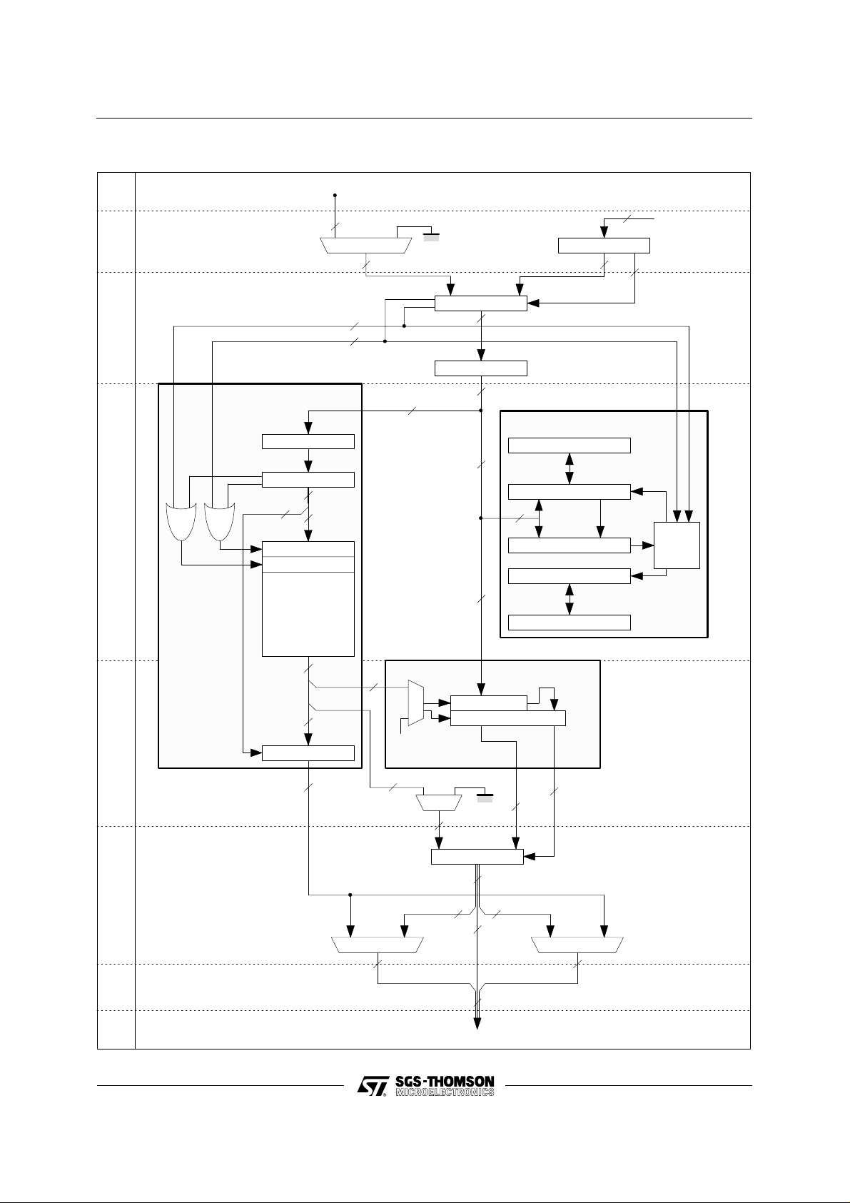
Figure 4 : Detailed Block Diagram of the Back end Post -pr ocessing Unit
SUNSTAR传感与控制 http://www.sensor-ic.com/ TEL:0755-83376549 FAX:0755-83376182 E-MAIL:szss20@163.com
SUNSTAR自动化 http://www.sensor-ic.com/ TEL: 0755-83376489 FAX:0755-83376182 E-MAIL:szss20@163.com
IMSA110
Clock
cycle
1
2
3
Cascade input pads
22
negative overflow
positive overflow
DATA TRANSFORMATION
UNIT
Prescaler
Over/under select
(Isbs) 2
64 x 32 bit RAM
8
6
USR
LSR
MUX
22
1
1
22
Cascade Adder
22
Rectifier
22
22
X bus
22
Shifter [8:0]
22
STATISTICS MONITOR
Min/max buffer
Min/max register
22
Comparator GT/LT
Over/undershoot count
Over/undershoot buffer
22
1
Rounding
From MAC array
Control
Y bus
32
[26:22]
[21:0]
32
4
Byte select
8
5
MUX
from
BCR
22
MUX
22
DATA NORMALIZER
Shifter -2 to 14
Zero data
1
22
Rounding
Output Adder
22
5
[21:14] [7:0]
MUX MUX
88
[21:14] [7:0]
88
6
[13:8]
6
22
Cascade output pads
A110-05.EPS
7/26

IMSA110
SUNSTAR传感与控制 http://www.sensor-ic.com/ TEL:0755-83376549 FAX:0755-83376182 E-MAIL:szss20@163.com
SUNSTAR自动化 http://www.sensor-ic.com/ TEL: 0755-83376489 FAX:0755-83376182 E-MAIL:szss20@163.com
Overflows
Bit 22 of the MMR records the history of positive
overflows on the X bus. S imilarly bit 23 records the
history of negative overflows. These bits in the
MMR are set to zero by writing to the MMR copy
location and are active independently of whether
the Static Threshold bit is set. When the MMR is
read, then bits 22 and 23 are interpreted as follows:
bit 23 bit 22 condition
0 0 No overflow has occured
0 1
1 0
1 1
One or more positive overflows
have occured
One or more negative overflows
have occured
Both postive and negative
overflows have occured
Detailed block diagram of the Backend P ost-processing Unit
Access to registers
The MMR and OUC are accessed, through the
memory interface, only via their associate d buffers
(MMB and OUB respec tively) and ar e not acc ess ible directly . In order to load the MMR with a value,
the host must first write the value to the MMB and
then transfer the data from the MMB to the MMR
by performing a WRITE to the co py MMR loc ation,
0B4
. To read the MMR the host must firs t perform
16
a READ cycl e from locat ion 0B4
(which transfer s
16
the contents of the MMR into the MMB) and then
read the MMB. The OU B is accessed in the same
way except that the dummy writes and reads are
done to and from location 0BC
16
.
Copies from MMR to MMB and OUC to OUB
(reads) can be performed at any time giving a
snapshot of the contents of the MMR and OUC
respectively. Copies from MMB to MMR and OUB
to OUC (writes) c an also be perf ormed at any time
allowing the threshold and counter to be updated
dynamically.
5.3 Data transformation unit
The data transformation unit consists of a prescalar, an under/over select detector, a look up table
and a byte selector. It can be used in isolation to
perform abitrary data mappings, or in conjunction
with the dat a normaliser to implement sophisticated
dynamic range compressi on functions .
Prescalar
This allows an 8-bit field anywhere within the 22-bit
X bus to be select ed as the address to the LUT. This
is performed by right shifting the X bus so that the
required 8 bits are at the least significant end. Th e
amount of right shift is programmed in BCR2[4-0]
and can have a value from 0 to 16.
Over/under select detector
With PosLUTAddr (SCR[6]) set to zero, this unit
monitors whether the amount of right shift performed by the prescalar is sufficient to include all
significant bits in, and maintain the sign of, the
selected 8 bit field (i.e. an over or under select is
generated if the most significant bit of the selecte d
8 bit field differs from any subse quent bit right up to
and including the most significant bit of the right
shifted X bus). This will be an ove rselect if the X
bus is positive (Bit 21 = 0), and an underselect if
the X bus is negative (Bit 21 = 1). In other words
the LUT address is always deemed to be signed
with an address range of -128 to 127.
If however the control bit PosLUTAddr (SCR[6]) is
set to one, the unit monitors whether the amount of
right shift performed by t he prescaler is suf ficient to
include all significant bits in the selected 8 bit field
AND that all unselected bits are zero (i.e. an over
or under select is generated if the first selected bit
(bit 9) is not zero OR differs from any subsequent
bit right up t o and including the most significant bit
of the right shif ted X bus). This w ill be an overselect
if the Xbus is positiv e and an underselect WHENEVER the Xbus is negative. Thus, in this mode, the
address range of the LUT is 0 to 255.
Prescalar under/over selects and X bus positive/negative overflows are passed to the LUT
along with the selected 8 bit address field.
Look up table (LUT) an d byte sel ect
The LUT consis ts of 64 words, 32 bits wide plus two
special 32 bit locations called t he upper and lower
saturation registers (USR and LSR respectively).
Thus the LUT is actually 66 words by 32 bits. The
32 bit output of the LUT is called the Y bus.
The most significant 6 bits of t he 8 bit address f ield
are used to address one of 64 words in the LUT.
The least significant pair of bits in the 8 bit field are
used to control a byte select on the output. Thus in
addition to operating as a 64+2 word look up table
of 32 bit words, it can be used as an 8 bit, 256+2
byte LUT prov iding 8bit — 8bit tr ansf orm ations .
Positive overflows on the X bus, and over selects
in the prescalar cause the LUT to access the USR
overriding the address given by the prescalar. Likewise negative overflows and under selects cause
the LUT to access t he LSR. Any sort of overflow on
the X bus or prescalar will cause the byte select
control to be overridden and the most significan t
byte (byte 3) of the appropriate Sat uration Register
will appear on the byte wide output of the data
transformat ion unit.
8/26

IMSA110
SUNSTAR传感与控制 http://www.sensor-ic.com/ TEL:0755-83376549 FAX:0755-83376182 E-MAIL:szss20@163.com
SUNSTAR自动化 http://www.sensor-ic.com/ TEL: 0755-83376489 FAX:0755-83376182 E-MAIL:szss20@163.com
If there are simultaneous overflows on the X bus
and in the prescalar then the overflow from the X
bus takes priority.
The USR and LSR can thus be used to model the
saturating behaviour of analogue circuits ins tead of
the usual ‘wrap around’ encountered in digit al s ystems. Alternat ively the USR and LSR could signal
error conditions within the backend directly on the
output pins via one of the output multiplexers.
The LUT is loaded via the memory interface. The
addressing for the LUT corresponds to the 8 bit
field, assuming that the byte s elector is being used.
In order to access the look up table, USR and LSR
from the microprocessor interface, the LUT Ac-
cess control bit ACR[1] must be set to zero. This
will force the Y bus to zero and the normaliser to be
controlled by BCR3[7-3] regar dless of the setting of
the dynamic normalisation bit, BCR3[2]. The LUT,
USR and LSR can then be loaded with any arbitrary
value via the microprocessor int erf ace. Set ting t he
LUT access control bit to one will then allow the LUT
to be used in the data transformation unit .
5.4 Data normaliser
This unit consis ts of a shifter capable of right shifts
of up to 14 bits and left shifts up to 2 bits, followed
by a
zero data unit
and an adder. The shifter is
controllable from one of two 5 bit sources : control
bits BCR3[7-3] or bits 26 to 22 of the Y bus. The
control bit Enable Dynamic Normalisation
(BCR3[2]) deter mines which s ource is in cont rol of
the normaliser . If this bit is set to zero the normaliser
is controlled by BCR3[7-3]. The five bit field is a
twos complement number between 14 and -2. This
indicates the amount of right shift (negative meaning left shift). Any value outside this range causes
the output of the shifter to be forced to zero. The
output of the shifter, with any rounding generated
by the shifter , goes int o the output adder.
5.5 Output adder
This is a 22 bit adder with one of its inputs coming
from the data normaliser. The other input is either
bits 21 to 0 of the Y bus f rom the data transformati on
unit, or set to zero under the control of BCR3[1].
Note that any overflow occuring due to left shifti ng
in the normaliser or the subsequent addition in the
output adder is not detected by the IMSA110.
5.6 Output multiplexers
These two mult iplexers allow the current ly selecte d
byte from the LUT to be optionally selec ted t o drive
either the most significant byte and/or the least
significant byte of the Cascade Out put pins. This is
controlled by the state of BCR2[5] and BCR2[6].
Enabling either of these mult iplexers over rides th e
state of the Cascade Output pins only on the relavent 8 pins. The remaining pins will continue to
represent the output of the output adder.
6. BACKEND POST-PROCESSOR — Modes of
Operation
The backend post-processing unit is capable of
performing many functions including data scaling,
transformation, dynamic range compression and
histogram equalisation.
6.1 Default mode (after Reset)
At power up or after reset the st ate of the bac kend
post-processor is such that data from the MAC
array and the cascade input are added and pass
straight through the datapath unaf fec ted.
The default mode for the statistics monitor is min
register although the values in the OUB, OUC,
MMR and MMB will be undefined. Likewise the
contents of the LUT, USR and LSR will be undefined, the LUT Access control bit will be zero
forcing the Y bus to zero and allowing the microprocessor interface to access the LUT, USR and
LSR.
Note that the cascade output pins and the PSR
output pins are tristated.
6.2 Cascade adder / MAC data scalar
These units allow the cascading of IMS A110s
where the output of the MAC array may be scaled
before it is added to the cascade input data. The
shifter can also be used for combining devices to
obtain extended precision in input data, coeff icient
word length or both.
The ability to zero the cascade input provides a
simple means of controlling the number of ‘active’
devices cascaded as well as a means of debugging
large systems.
6.3 Rectification
Rectification, the removal of negative results, is
needed in several image processing functions.
For example, e dge detection us ing a Sobel operator usually requires full wav e rectification due to the
different signs obtained at differing edge transitions. Edge detection using a Laplacian operator
produces a change of sign at an edge. In this case,
removing negative numbers using half wave rectification can produce better results as full wave
rectification can lead to some blurring of the edge
transition.
9/26

IMSA110
SUNSTAR传感与控制 http://www.sensor-ic.com/ TEL:0755-83376549 FAX:0755-83376182 E-MAIL:szss20@163.com
SUNSTAR自动化 http://www.sensor-ic.com/ TEL: 0755-83376489 FAX:0755-83376182 E-MAIL:szss20@163.com
6.4 Static scal in g
This can be performed using one of two units: the
MAC array output shifter (as above), and the data
normaliser . In the second case the data undergoes
a simple scaling operation (with rounding) within
the normaliser . The normaliser can be used to scale
(multiply) the data by the factors 0, 1/16384,
1/8192, 1/4096 ..., 1/2, 1, 2, 4. By controlling the
normaliser from the control bits BCR3[7-3], this
provides a means for simple scaling of the data
before it is output . Set ti ng BCR3[ 1] and B CR2[ 6,7]
to zero ensures that the data transformation unit
takes no part in the operation and the output of the
normaliser is passed unchanged to the output pins.
6.5 Dynamic scal ing
In this mode the scaling is controlled by the data
itself. i.e. the scalar is controlled from the LUT
(Ybus bits 26-22) by setting BCR3[2] to one, the
Ybus input to the output adder being set to zero
either by setting BCR3[1] to zero or programming
the LUT accordingly. This mode can provide a
discontinuous non-linear transformation.
6.6 Simple t ran sfo rmati o n
This mode allows the user to apply arbitrar y trans formations to the data before it is output. Here the
LUT is treated as 256 by 8, addressed as either
-128 to 127 if PosLUT Addr is set to zero or 0 to 255
if PosLUT Addr is set to one. The 8 bit field selected
by the LUT prescalar is used to address a byte in
the LUT which is passed dir ect ly to t he out p ut pins
via one of the output multiplexers. Ybus control of
the data normaliser is disabled, BCR3[7-3] are set
out of range so as to zero t he normaliser output and
the Ybus input t o the output adder is set to zero by
BCR3[1]. One (or both) of the output multiplexers
are enabled and so the addressed byte from the
LUT passes straight to the cascade output pads.
Only the most signif icant byt e of the USR and LS R
are applicable in this mode as overflows override
the byte select control and force it to select the most
significant byte.
6.7 Dynamic normalisation
In this mode the normaliser and transformation
units in the outp ut condit ioner are used t ogether to
perform sophisticated non-linear dynamic range
compression and trans formations. As in the s imple
transformatio n case the prescalar selects an 8 bit
field anywhere within the X bus. The most significant 6 bits, and overflows, are fed as an address to
the LUT. In this case the look up table is treat ed as
64+2 by 32. Bits 26 to 22 of the Y bus are used to
control the normaliser block so that the input to the
normaliser is dy namically s caled. The out put of t he
normaliser is then added in the output adder to the
least significant 22 bits of the Y bus (Note t hat only
28 bits of the 32 bit Y bus are actually used).
Thus the data is scaled, rounded, and then an of fset
is added to the scaled result. Each operation can
be viewed as
output = input × scale + offset
Where scale and offset are both programmable
functions of input. One way to view this operation
is to consider that the original data r ange is divided
into 64 equal sized levels and in each level a
different scale and off s et is applied. The s cale and
offset stored in the US R and LSR would be chosen
to give the desired behaviour under overflow conditions.
Note that in the case of cascade adder overflows,
the data on the X bus is invalid, so the scale here
would usually be set out of range so as to zero the
normaliser output. The offs ets in the USR and LSR
would then provide the cascade outp ut directly.
Note also that if the 5 bit scale field in the LUT is
programmed so that the normaliser always zeros
the data, then the output will correspond to the 22
bit offset field in the LUT. This can be viewed as a
coarse transformation with wide dynamic range
which is useful for applications such as image
contour emphasis and equalisat ion.
Figure 5 : Bit Format of Dat a Stored in LUT, USR and LSR
31 24 23 16 15 8 7 0
scale if
BCR3 [2] = 1
10/26
offset if BCR3 [0] = 1
BYTE 0BYTE 1BYTE 2BYTE 3
A110-06.EPS

IMSA110
SUNSTAR传感与控制 http://www.sensor-ic.com/ TEL:0755-83376549 FAX:0755-83376182 E-MAIL:szss20@163.com
SUNSTAR自动化 http://www.sensor-ic.com/ TEL: 0755-83376489 FAX:0755-83376182 E-MAIL:szss20@163.com
7. GLOSSARY
This section defines the meaning of terms used
elsewhere in this data sheet.
Arithmetic S hift
For a right shift, the most significant bit is always
copied into the most significant end of the result.
For example shifting right by 2:
01000101
11000101
→
→
00010001
11110001
For a left shift, the least significant bit will become
zero.
Note that left shifting can cause overflows and
these are not detected in the MAC output scalar or
the data normaliser.
Rounding
All rounding done within the IMS A1 10 is equivalent
to truncating after adding 1/2 LSB. (Rounding is
always applied in the posit ive direction). For example for 8 bit t wos complement numbers underg oing
a two bit right shift:
00000011→00000000 + 1 = 00000001 (rounded up)
00000010→00000000 + 1 = 00000001 (rounded up)
11111110→11111111 + 1 = 00000000 (rounded up)
00000001→00000000 (no rounding)
11111101→11111111 (no rounding)
Left shifts do not generat e rounding.
Tran sversal Fi lter
A trans versal f ilter is a calculat ion c onsist ing of the
sum of products of succes sive points of input data.
For input data x
c
, ..., the result, Y is:
6,c5
, x
, ..., an d a set of coefficients,
i
i+1
6
Y=∑c
× x
i
6−i
i=0
T w o’s Complement
Two’s complement numbers allow both positive
and negative numbers. For example in 8 bit numbers the most positive number is 127, the most
negative is -128:
two’s complement decimal
10000000 -128
10000001 -127
11111111 -1
00000000 0
00000001 1
01111111 127
Rectification
Rectification is a method of removing negative
numbers. There are two methods: Full wave and
Half wave. In either case all positive numbers and
zero are unaffected. In Full wave rectification, any
negative numbers are negated (i. e. multiplied by 1)
so that they become positive. In Half wave rectification, all negative numbers are replac ed by zero.
Dynamic Range Comp ressi on
When Dynamic is used in this context, it is to
indicate a change of behaviour for each data point.
For example, a dynam ic shift is one where the size
of the shift may change on each successive clock
cycle. Dynamic range compression is range compression making use of an offset and shift, which
can change depending on each data point. This
allows the essential non-linear transformations required in image processing to be implemented on
the IMS A1 10.
Bit Fields
Bits, words and addresses in this data sheet are
little-endian; The lowest order byte of a multiple
byte word is referred to as byte 0, and is a ddressed
in the same way. Similarly, the least significant bit
of any bit field is that with the lowest bit number . For
example, ‘bits 26-22’ ref ers to a 5 bit field where bit
22 is treated as the least significant, and bit 26 as
the most signific ant.
Latency
Within the IMSA110 the latency is the number of
clock cycles from an input to its corresponding
output. For instance, with the programmable shift
registers bypassed by setting SCR[1] to 1, the
latency from PSRin to PSRout will be 2 as shown
in Figure 6.
11/26

IMSA110
SUNSTAR传感与控制 http://www.sensor-ic.com/ TEL:0755-83376549 FAX:0755-83376182 E-MAIL:szss20@163.com
SUNSTAR自动化 http://www.sensor-ic.com/ TEL: 0755-83376489 FAX:0755-83376182 E-MAIL:szss20@163.com
Figure 6
123
CLK
PSRIN
PSROUT
PSRIN latched
PIN DESIGNATIONS
System services
Pin In/out Function
VCC, GND Power supply and return
CLK in Input clock
RESET in System reset
Synchronous input/output
Pin In/out Function
PSRin[7-0]
PSRout[7-0]
Cin[21-0] in Cascade input port
Cout[21-0] out Cascade output port
Programmable shift register
in
input
Programmable shift register
out
output
As yn c h r onous in put/o utput
Pin In/out Function
E1, E2
W
ADR[8-0] in Memory interface adress bus
D[7-0] in/out Memory interface data bus
Note : Signal names are shown with an overbar if they are active
low, otherwise they are active high.
Memory interface enable
in
signals
Memory interface write
in
enable
8.1 System se rvice s
System serv ices include all the necessary logic to
start up and maintain t he IMS A110.
Power
Power is supplied to the device via the V
CC
and
GND pins. Several of each are provided to mini-
mise inductance within t he package. All supply pins
must be connected. The supply must be decoupled
close to the chip by at least one 100nF low inductance (e.g. ceramic) capacitor between V
CC
and
GND.
CLK
The clock signal CLK controls the timing of input
and the output on the four dedicated interfaces, and
controls the progress of data t hrough the s hift re gisters, multiply-accumulate array and post-processing unit. The A1 10 is fully stat ic so the clock c an
be slowed down or sto pped in either state without
corrupting data.
RESET
If this pin is taken low for at least 2 clock cy cles, the
control logic within the IMS A110 will be reset and
all of the control and configuration register s will be
initialised to their default values. All other register,
memory locations, dat apath registers and shift registers will not b e reset by this signal.
A reset is i nitiated aut omatically when pow er is first
applied to the device. This reset will be c ompleted
once four cycles of CL K have occured after VCC is
valid.
8.2 Synchro nou s services
PSRin[7-0]
This 8-bit wide bus supplies input data to the device. The input data ent ers the first of the three shif t
registers in the chain. The timing of this input is
controlled by the CLK signal. The data on the
PSRin port is sampled on the rising edge of the
clock. In a cascade arrangement, this bus will be
connected to the PSRout port of the previous de-
vice. In such an arrangement the PSRin port on the
first device will be the input to the overall cascaded
system.
A110-07.EPS
12/26

IMSA110
SUNSTAR传感与控制 http://www.sensor-ic.com/ TEL:0755-83376549 FAX:0755-83376182 E-MAIL:szss20@163.com
SUNSTAR自动化 http://www.sensor-ic.com/ TEL: 0755-83376489 FAX:0755-83376182 E-MAIL:szss20@163.com
PSRout[7-0]
This bus outputs the data from th e last programmable shift register in the chain. The data on this bus
is synchronously cl ocked by the rising edge of CLK .
In a cascade arrangement this port will be connected to the PSRin port of the next device. At
power up, or after a reset, the PSRou t pins are
tristated. They are enabled by SCR[ 5] .
Cin[21-0]
The Cascade Input port allows IMSA110s to be
cascaded. It also can be used for combining an
external signal (e.g. a r eference image or an of fset)
with the processed result. In a cascade arrangement, this bus will be connected to the Cascade
Output of the previous device. T he data on the Cin
bus is sampled on the rising edge of CLK.
Cout[21-0]
This bus outputs the processed result from the
IMSA110 and can also be used for cascading. The
22-bit result is synchronous ly c locked by the r ising
edge of CLK. In a typical cascaded system this bus
will be connected to the Cascade Input port of the
next device. On the last device in the cas cade, this
bus will be the output of the overall system. At
power up, or after a reset, the Cout pins are tris-
tated. They are enabled by S CR[ 4].
8.3 Asynchro no us in put/o utp ut
E1, E2
If both of these signals are low , then the microproc essor interface is enabled. The operation of these
enable signals is very similar to those found on
static RAMs. When either of these s ignals are high
the Write Enable and the address inputs are ignored and the microprocessor interface Data signals are high impedance. When both Enable signals are low a read or write access is made to
registers or the RAMs within the IMSA110. Access
to the microprocessor interface can occur asynchronously to the synchronous pins (PSRin,
PSRout, Cin, Cout) of the device.
W
Write Enable indicates whether the access to the
IMS A110 memory interface is to be a read or a
write. If
W is low a write access is indicated.
ADR[8-0]
The nine bit binary value applied to the address
inputs of the IMSA110 indicates which register or
RAM location within the device is to be accessed.
D[7-0]
During a write to the microprocessor interface an
8-bit word is applied to the Data pins which is
written to the appropriate location. During a read
cycle the contents of the location accessed are
placed on the Data pins. When either of the Enables are high the Data pins are high impedance.
9 REGISTE R DE SCRI P T ION
Memory map
Within the IMSA110 addresses are fully decoded.
Reading from locations not defined in the memory
map will produce zero data. Data written to such
locations is ignored. T his allows the part t o be fully
programmed using a ROM with an address incremeter. In this case, for future compatibility, zero
should be written to all undefined locations.
13/26

IMSA110
SUNSTAR传感与控制 http://www.sensor-ic.com/ TEL:0755-83376549 FAX:0755-83376182 E-MAIL:szss20@163.com
SUNSTAR自动化 http://www.sensor-ic.com/ TEL: 0755-83376489 FAX:0755-83376182 E-MAIL:szss20@163.com
Register Address decimal Address hex Function
CR0a 0—6 000—006 Coefficient Registers Bank 0a
CR0b 16—22 010—016 Coefficient Registers Bank 0b
CR0c 32—38 020—026 Coefficient Registers Bank 0c
CR1a 64—70 040—046 Coefficient Registers Bank 1a
CR1b 80—86 050—056 Coefficient Registers Bank 1b
CR1c 96—102 060—066 Coefficient Registers Bank 1c
PCRA 128—129 080—081 PSRA Control Register
PCRB 130—131 082—083 PSRB Control Register
PCRC 132—133 084—085 PSRC Control Register
SCR 144 090 Static Control Register
ACR 146 092 Active Control Register
BCR 160—163 0A0—0A3 Backend Configuration Register
MMB 176—178 0B0—0B2 Maximum/Minimum Buffer
CMM 180 0B4 Copy MMR
OUB 184—186 0B8—0BA Overshoot/Undershoot Buffer
COU 188 0BC Copy OUC
TCR 208 0D0 Test Control Register
USR 248—251 0F8—0FB Upper Saturation Register
LSR 252—255 0FC—0FF Lower Saturation Register
LUT 256-511 100—1FF Look up Table
9.2 Regist ers
CR0a Coefficient registers bank 0a
These seven 8-bit locations contain coefficients
which can be used by the third, of the three, 7-stage
mac arrays. CR0a(0) (address #000) corresponds
to the coeffici ent register of this mac ar ray neares t
to its output. Similarly CR0a(6) (address #006)
corresponds to the coefficient register of thi s mac
nearest to its input . These Coef fic ient r egisters can
be written to provided that the other register bank
is in use. Whether the coefficient written is signed
or unsigned is determined by the ‘Unsigned Coefficient’ bit SCR[3]. Once a value is written to a
coefficient register , its value can be read back from
an internal duplicate register. These registers will
be used by the mac array, when ACR[0], ‘Current
Bank’ is set to zero. Writing to these Coefficient
Registers while in use will result in an undefined
operation of the mac array.
CR0b Coefficient reg isters ban k 0b
These seven 8-bit locations contain coefficients
which can be used by the second, of the three,
7-stage mac arrays in the chain. CR0b(0) (address
#010) corresponds to t he coef ficient register of t his
mac array n earest to its output. Similarly CR0b(6)
(address #016) corresponds to to the coefficient
register of this mac nearest to its in put. Their behaviour is otherwise identical t o CR0a.
14/26

IMSA110
SUNSTAR传感与控制 http://www.sensor-ic.com/ TEL:0755-83376549 FAX:0755-83376182 E-MAIL:szss20@163.com
SUNSTAR自动化 http://www.sensor-ic.com/ TEL: 0755-83376489 FAX:0755-83376182 E-MAIL:szss20@163.com
Figure 7 : I M SA 110 Memory Map
Address
(Hex) 7 6 543210
1FF
100
0FC-0FF LSR Lower Saturation Register
0F8-0FB USR Upper Saturation Register
0D0 TCR
0BC COU Copy Over/UnderShoot Buffer
0B8-0BA OUB Over/UnderShoot Buffer
0B4 CMM Copy Min/Max Buffer
0B0-0B2 MMB Min/Max Buffer
0A3 BCR3 Normaliser Control
0A2 BCR2 0
0A1 BCR1 000000
0A0 BCR0
092 ACR 000000
090 SCR 0
085 PCRC 0 0 0 0 0 Shift Length (Upper Bits)
084 PCRC Shift Length (Lower Bits)
083 PCRB 000
082 PCRB Shift Length (Lower Bits)
081 PCRA 0 0 0 0 0 Shift Length (Upper Bits)
080 PCRA Shift Length (Lower Bits)
066
...
060
Name
LUT Look Up Table
LS
output
byte
Full
Wave
CR1c Bank 1 Coefficient Register
Half
Wave
PosLUT
Addr
MS
output
byte
PSR Out
Enable
Cascade
Enable
0
bit
Look Up Prescaler
MAC Output Scaler
Unsigned
Coef
Load
Unsigned
0 Shift Length (Upper Bits)
Dynamic
normali-
sation
Data
LUT to
output
adder
Static
threshold
Backend
LUT
Access
Bypass
PSRs
0
Greater
Than
Zero
Cascade
Current
Bank
Cont
Swap
056
...
050
046
...
040
026
...
020
016
...
010
006
...
000
CR1b Bank 1 Coefficient Register
CR1a Bank 1 Coefficient Register
CR0c Bank 0 Coefficient Register
CR0b Bank 0 Coefficient Register
CR0a Bank 0 Coefficient Register
15/26

IMSA110
SUNSTAR传感与控制 http://www.sensor-ic.com/ TEL:0755-83376549 FAX:0755-83376182 E-MAIL:szss20@163.com
SUNSTAR自动化 http://www.sensor-ic.com/ TEL: 0755-83376489 FAX:0755-83376182 E-MAIL:szss20@163.com
CR0c Coefficien t registers bank 0 c
These seven 8-bit locations contain coefficients
which can be used by the first , of the three, 7-st age
mac arrays in the chain. CR0c(0) (address #020)
corresponds to the coefficient register of this mac
array nearest to its output. Similarly CR0c(6) (address #026) corresponds to to the coefficient regis ter of this mac nearest to its input . Their b ehaviour
is otherwise identical to CR0a.
CR1a Coefficien t registers bank 1 a
These seven 8-bit locations contain coefficients
which can be used by the t hird, of the three, 7-st age
mac arrays in the chain. CR1a(0) (address #040)
corresponds to the coefficient register of this mac
array nearest to its output. Similarly CR1a(6) (address #046) corresponds to to the coefficient regis ter of this mac nearest to its input. These regis ter s
will be used provided that ACR[0], ‘Cur rent Bank’ is
set to one, or continuous bank swap mode is in
operation (SCR[0] set t o one).
CR1b Coefficient r egisters bank 1b
These seven 8-bit locations contain coefficients
which can be used by the second, of the three,
7-stage mac arrays in the chain. CR1b(0) (address
#050) corresponds to the coef ficient regist er of this
mac array nearest to its output. Similarly CR1b(6)
(address #056) corresponds to to the coefficient
register of this mac nearest to its input. Their behaviour is otherwise identical to CR1a.
CR1c Coefficien t registers bank 1 c
These seven 8-bit locations contain coefficients
which can be used by the second, of the three,
7-stage mac arrays in the chain. CR1c(0) (address
#060) corresponds to the coef ficient regist er of this
mac array nearest to its output. Similarly CR1c(6)
(address #066) corresponds to to the coefficient
register of this mac nearest to its input. Their behaviour is otherwise identical to CR1a.
PCRA PSRA Control regi ster
This is a 16-bit register, with least significant byte
at location #080, and is us ed to set up the lengt h of
the last shift register in the chain. Programmed
lengths outside the range 0 to 1120 will cause
undefined behaviour of the shift register.
PCRB PSRB Control register
This is a 16-bit register, with least significant byte
at location #082, and is us ed to set up the lengt h of
the second shift register in the chain. Program med
lengths outside the range 0 to 1120 will cause
undefined behaviour of the shift register.
PCRC PSRC Control register
This is a 16-bit register, with least significant byte
at location #084, and is used to set up the length of
the first shift register in the chain. Programmed
lengths outside the range 0 to 1120 will cause
undefined behaviour of the shift register .
SCR Static control register
The Static Control Register contains the cont rol bits
which set up parts of the IMS A110 which are likely
to not need reconfigurat ion during processing. The
contents of this register are not affected by the IMS
A110 and can be read at any time. Modifying the
Static Control regis ter during process ing will result
in undefined behaviour . Normal operation w ill start
to occur between 0 and 3 clock cycles after the
completion of the write cy cle.
ACR Active control register
The Active Control Register contains status and
control bits which are likely to be accessed during
normal operation of the IMS A1 10.
BCR Backend configuration register
The Backend Configuration Registers consist of
four byte-wide registers BCR0, BCR1, BCR2, and
BCR3 which are located at address es #0A0, #0A1,
#0A2, and #0A3 respectively. These four registers
are used to control the backend post-processing
unit. None of the control bits in these r egist ers c an
be modified by the IMS A110. Modification of the
values in these registers during processing may
result in undefined behaviour. Normal operation will
start to occur bet ween 0 and 3 clock cycles af ter the
completion of the write cy cle.
MMB Maximum/minimum buffer
These three locat ions hold a 24-bit wide word, with
the least significant byte at the lowes t address, a nd
act as a buffer between the MMR and the microprocessor interface. All the transactions between
the MMR and the host processor must take place
through this register. When the MMR is not in use,
the value of this buffer is undefined.
CMM Copy MMR
This location is used to enable the data transfer
between the MMB and MMR. A write to this location
causes the contents of MMB to be copied into the
MMR and bits 23 and 22 of the MMR (the cascade
adder overflow flags) to be set to zero. A read from
this location ca uses the revers e, i.e the cont ents of
the MMR are copied into the MMB. The value
written to this location is ignored, the value read
back is undefined.
16/26

IMSA110
SUNSTAR传感与控制 http://www.sensor-ic.com/ TEL:0755-83376549 FAX:0755-83376182 E-MAIL:szss20@163.com
SUNSTAR自动化 http://www.sensor-ic.com/ TEL: 0755-83376489 FAX:0755-83376182 E-MAIL:szss20@163.com
OUB Overshoot /undershoot buffer
These three memory locations hold a 22-bit word,
with the least significant byt e at the lowest address,
and act as a buffer between the OUC and the
microprocessor interface. All the transactions between the OUC and the host processor must take
place through this register . W hen the O UC is not in
use, the value of this buffer is undefined.
COU Copy OUC
This location in the memory is used to enable the
data transfer between the OUB and OUC. A write
to this location causes the contents of OUB to be
copied into the OUC. A read from this location
causes the reverse, i.e t he contents of the OUC are
copied into the OUB. The value written to this
location is ignored, the value read back will be
undefined.
TCR Test con tro l regist e r
This register is used for testing, and should be
loaded with zero for normal operation.
USR Upper saturation regi ster
This is a 32-bit value with the least significant byte
at the lowest address. Its contents are used to
replace the LUT output if positive overf low(s) occur
in the look up prescaler and / or in the cascade
adder. Accesses f rom the microprocessor interface
can only be made while ACR[1] is set to zer o.
LSR Lower saturation regist er
This is a 32-bit value with the least significant byte
at the lowest address. Its contents are used to
replace the LUT output if negative overflow(s) occur
in the look up prescaler and / or in the cascade
adder. Accesses f rom the microprocessor interface
can only be made while ACR[1] is set to zer o.
LUT Look up table
These locations are for the 256-byte look up table
which is used for dat a mapping and tr ansformati on
operations. From the microprocessor interface,
these locations are addressed in the s ame way as
that seen by the 8-bit output of look up prescaler.
When used in 32 bit mode, the locations are treate d
in the same way as other 32 regist ers : W ord 0 has
its most significant by te at #103, its least significant
byte at # 100, W or d 12 has its mos t signif ic ant byt e
at #133, its least significant byte at #130. Accesses
from the microprocessor interface can only be
made while ACR[1] is s et t o zero.
10. REGISTERS — BIT ALLOCA TION
This section descri bes the register details bit by bit.
Each section commences with the name of the
register with the bit number(s) followed by the default value, in the general format:
Name REGISTER [MSB—LSB] Default : MSB...LSB
The least significant bit of a register is bit 0.
* in the tables indicates the default state of the
register bit(s).
10.1 PSR control registers (PCR)
PSRA control PCRA[10-0] Default: 0……0
These eleven least significant bits of the PCRA are
used to specify the length of the last Programmable
Shift Register (PSRA). The length of the shift register will be numerically equal to the binary value
loaded in these bits. The value loaded in must be
in the range of 0 to 1120 decimal. If a v alue outside
this range is written to these bits the behaviour of
the shift register will be undefined. After updating
this register , the behaviour of the delay is undefined
for 22 clock cycles. Hence changing the length from
1000 to 1001 delays, will result in correct output
only after 1023 cycles. This w ill also have to propagate through the backend before the cascade out put values will be correct.
Reserved PCRA[15-11] Default: 00000
These 5 most significant bits of the PCRA are
reserved. The user should write zero to these locations to maintain compatibility with futur e products.
The value read from these locations will be zero.
17/26

IMSA110
SUNSTAR传感与控制 http://www.sensor-ic.com/ TEL:0755-83376549 FAX:0755-83376182 E-MAIL:szss20@163.com
SUNSTAR自动化 http://www.sensor-ic.com/ TEL: 0755-83376489 FAX:0755-83376182 E-MAIL:szss20@163.com
PSRB control PCRB[10-0] Default: 0……0
These eleven least significant bits of the PCRB are
used to specify the length of the second Programmable Shift Register (PSRB). The lengt h of the shift
register will be numerically equal to the binary value
loaded in these bits. The value loaded in must be
in the range of 0 to 1120 decimal. If a value outside
this range is written to these bits the behaviour of
the shift register will be undefined. After updating
this register will also have to propagate through
PSRA and t he backend before the c asc a de output
values will be correct
Reserved PCRB[15-11] Default: 00000
These 5 most significant bits of the PCRB are
reserved. The user should write zero to these locations to maintain compatibility with future pr oducts.
The value read from thes e locat i ons will be z ero.
PSRC control PCRC[10-0] Default: 0……0
These eleven least significant bits of the P CRC are
used to specify the length of the first Programmable
Shift Register (PSRC). The length of the shift register will be numerically equal to the binary value
loaded in these bits. The value loaded in must be
in the range of 0 to 1120 decimal. If a value outside
this range is written to these bits the behaviour of
the shift register will be undefined. After updating
this register will also have to propagate through
PSRB, PSRA and the backend before th e cascade
output values will be correct
Reserved PCRC[15-11] Default: 00000
These 5 most significant bits of the PCRC are
reserved. The user should write zero to these locations to maintain compatibility with future pr oducts.
The value read from thes e locat i ons will be z ero.
10.2 Static co ntrol register (S C R)
Reserved SCR[7] Default: 0
This location is reserved. The user should write
zero to this locatio n to maintain compatibility with
future products. The value read from this location
will be zero.
Positive Look up
table address
SCR[6] Default: 0
This bit affects the way in which the over/under
select detector checks the LUT address. It determines whether the address range of the LUT is
signed (-128 to 127) or positive (0 to 255). A one at
this location indicates a posit ive LUT addres s.
PSR out Enable SCR[5] Default: 0
A zero at this location will force the PSR Output pins
into the tristat e mode.
Cascade Enable SCR[4] Default: 0
A zero at this location will force the Cascade Output
pins into the tristate mode.
Unsigned coefficient
load
SCR[3] Default: 0
If this bit is set to one, the format of subsequently
loaded coefficients become unsigned, with coefficient value assuming a range between 0 and 255
decimal. An 8-bit coefficient with all its bits set to
one will represent +255 decimal. When this bit is
zero the format of subsequently loaded coefficients
will be twos complement and the corresponding
numerical value will have a range between -128
and +127. By changing this bit whilst coefficients
are being loaded, coefficients between -128 and
+255 can be used. The unsigned format on all
coefficients is suitable when IMS A110s are combined to obtain wider coefficient s for extended precision.
SCR[3] Coefficient type
0 Signed coefficients *
1 Unsigned coefficients
Unsigned data SCR[2] Default: 0
If this bit is set to one, the IMS A110 input data
format will become unsigned, with input data value
assuming a range between 0 and 255 dec imal. An
8-bit value with all its bits set to one will represent
+255 decimal. When this bit is zero the input data
format will be twos complement and the corresponding numerical value will have a range between -128 and +127. Unlike SCR[ 3], this bit cannot
be used to dynamically alter the data format. The
unsigned format is suitable when IMS A110s are
combined to obtain wider input data for extended
precision.
SCR[2] Data type
0 Signed data *
1 Unsigned data
Bypass shift registers SCR[1] Default: 0
This bit is used to progra m the path between the
PSRin and PSR out ports. A z ero at this locat ion will
cause the output from the last programmable shift
register to be sent to P S Rout port . Wr iting a one t o
this bit will cause the three programmable shift
registers to be bypassed, and t he data entering the
port PSRin to be fed directly, via a delay of 2 clock
cycles, to the port PSRout. This bit allows full programmability of a cascade arrangem ent so that the
same hardware can be operated in a variety of
ways.
18/26

IMSA110
SUNSTAR传感与控制 http://www.sensor-ic.com/ TEL:0755-83376549 FAX:0755-83376182 E-MAIL:szss20@163.com
SUNSTAR自动化 http://www.sensor-ic.com/ TEL: 0755-83376489 FAX:0755-83376182 E-MAIL:szss20@163.com
Continous bank swap SCR[0] Default: 0
The continuous bank Swap bit selec ts whether the
the two banks of coefficient registers are used
alternately after each data input or if this is contr olled solely by the state of the ‘Cur rent Bank’ bit in the
Active Contr ol Regis ter ACR[ 0] .
SCR[0] Swap mode
0 Swap on asserting ACR[0] *
1 Swap after end of each input cycle
10.3 Active control register (ACR)
Reserved ACR[7-2] Default: 00000
These 6 most significant bits of the ACR are reserved. The user should write zero to these locations to maintain compatibility with future pr oducts.
The value read from thes e locat i ons will be z ero.
Enable look up table ACR[1] Default: 0
Writing a zero i nto this control bit allows the memory
interface to access the Look up table; the output t o
the data transformation unit will be zero. The normaliser will be controlled by BCR3[7-3], regardless
of the state of BCR3[2]. Writing a one to ACR[1]
allows the IMS A1 10 to use the Look up T able. After
changing this bit, 2 clock cyc les m ust occur bef ore
the Look up Table can be accessed.
full-wave rectified (absolute value operation) before it is fed to the remainder of the backend. This
bit will override the function of the BCR0[6].
Enable half-wave
rectification
BCR0[6] Default: 0
Writing a one in this bit will cause the negative
values from the cascade adder to be replaced with
zero. Note that writing a one into BCR0[7] will
override the function of this c ontro l bit.
BCD0[7-6] Rectifier mode
0 0 Straight through *
0 1 Half wave rectification
1 0 Full wave rectification
1 1 Full wave rectification
Mac array output
scaler
BCR0[5-1] Default: 00000
The contents of these five bits control the amount
of right or left shif t applied to the data at the output
of the mac array . This field is interpreted as a t wo’s
complement number. A positive number represents a right shift (divide). A ny shif t in the range -8
(1 1 000) to +8 (01000) is legal. Values outside this
range will result in undefined behaviour of the mac
output scaler.
Zero cascade input BCR0[0] Default: 0
ACR[1] LUT mode
0 Memory interface access *
1 Data transformation unit
Current bank ACR[0] Default: 0
When the ‘Continuous Bank Swap’ bit is set to zero,
writing a zero into this control bit instructs the IMS
A110 to use the set of coefficient registers at addresses 0 to #X26. Setting a one to t his bit instruc ts
the IMS A110 to use the set of c o eff icient registers
at addresses #40 to #X66. If the ‘Continuous Bank
Swap’ bit is set to one, then this bit only indicates
the bank selected for the first cycle of the continuous swap mode. Writing to this bit whilst in cont inuous bank swap mode (SCR[0]=1) will result in
undefined behaviour of the mac array.
ACR[0] Coefficient bank
0 Use coefficient registers at 0 to #X26 *
1 Use coefficient registers at #40 to #X66
10.4 Backend control regi ster 0 (BCR0)
Enable full-wave
rectification
BCR0[7] Default: 0
If this bit is set the output of the cascade adder is
This bit controls the Cascade Input Multiplexer.
Writing a one to this bit will cause a zero, instead of
the cascade input data, to be fed to the cascade
adder.
BCR[0] Cascade input mode
0 Cascade data *
1 Zero
10.5 Backend control register 1 (BCR1)
Reserved BCR1[7-2] Default: 00000
These locations are reserved. The user should
write zero to these locations to maintain compatibility with future products. The values read from
these locations will be zero.
Static threshold BCR1[1] Default: 0
If this bit is set to one, the signals from the c omp arator will be used to increment the Over / Undershoot Counter only. If this bit is zero, the signals
from the compar ator will be used to latch the output
of the Cascade Adder into the Max imum / Minimum
Register (MMR), and to increment the counter. In
this case the counter will have been incremented
by the number of times that the threshold has been
updated.
19/26

IMSA110
SUNSTAR传感与控制 http://www.sensor-ic.com/ TEL:0755-83376549 FAX:0755-83376182 E-MAIL:szss20@163.com
SUNSTAR自动化 http://www.sensor-ic.com/ TEL: 0755-83376489 FAX:0755-83376182 E-MAIL:szss20@163.com
Enable greater than BCR1[0] Default: 0
This control bit determines whether the comparator
in the statistic s monitor behaves as a ‘greater than’,
or as a ‘less than’ comparator. The signal from t his
comparator is used to drive the O ver / Undershoot
Counter and the Max / Min Register. A one at this
location selects ‘greater than’.
BCR1[1-0] Statistics monitor mode
0 0 Min. register *
0 1 Max. register
1 0 Undershoot counter
1 1 Overshoot counter
10.6 Backend control regi ster 2 (BCR2)
Reserved BCR2[7] Default: 0
This location is reserved. The user should write
zero to this locatio n to maintain compatibility with
future products. The value read from this location
will be zero.
Pass LUT data to
least significant
output
BCR2[6] Default: 0
This bit controls the output multiplexer . If this bit is
set to one, the selected byte from t he LUT is output
on the least significant byte (bits 7 to 0) of the
Cascade Output pins.
Pass LUT data to most
significant output
BCR2[5] Default: 0
This bit controls the output multiplexer . If this bit is
set to one, the selected byte from t he LUT is output
on the mos t significant byte (bits 21 to 14) of the
Cascade Output pins.
Look up prescaler BCR2[4-0] Default: 00000
The contents of these five bits control the amount
of (arithmetic) right shift applied to the dat a, by th e
Look up Prescaler. Writing a numerical value between 0 and 16 (binary 10000) into these bits, will
cause the data to be right-shifted by a corr esponding number of places. For example, if the bit pattern
00101 is written to these five bit positions, a right
shift of 5 plac es will occur . W riting any value out side
the range (0 to 16) will result in undefined behaviour
of the look up Prescaler .
10.7 Backend control register 3 (BCR3)
Normalizer control BCR3[7-3] Default: 00000
These five bits control the number of places, that
the normaliser shifts the data to the right or to the
left. This field is interpret ed as a twos complement
number. A positive number is taken to be a right
shift. Any shift in the range -2 (1 11 10) to +14 (011 10)
is legal. Any other value will cause the number zero
to be output from the normaliser.
Enable dynamic
normalization
BCR3[2] Default: 0
If this bit is set to one, the normaliser will be controlled by bits 26 to 22 from the output of the look
up table, instead of BCR3[7-3] .
Feed LUT data to
output adder
BCR3[1] Default: 0
One of the inputs of the Output Adder can be either
supplied by the Look up Table or forced to zero.
Setting this control bit to zero selects zer o. Setti ng
this control bit to one select s bits 21 to 0 of the Look
up Table.
Reserved BCR3[0] Default: 0
This location is reserved. The user should write
zero to this lo cation to maintain compatibility with
future products. The value read from this location
will be zero.
20/26

IMSA110
SUNSTAR传感与控制 http://www.sensor-ic.com/ TEL:0755-83376549 FAX:0755-83376182 E-MAIL:szss20@163.com
SUNSTAR自动化 http://www.sensor-ic.com/ TEL: 0755-83376489 FAX:0755-83376182 E-MAIL:szss20@163.com
11. ELECTRICAL SPECIFICATION
11. 1 DC electrical characteristi c s
ABSOLU TE MA XI M UM RATINGS
Symbol Parameter Min. Typ. Max. Units Notes (1,2)
V
CC
V
, V
I
T
A
T
stg
PDmax Power dissipation 2.0 W
Notes : 1. All voltages are with respect to GND.
2. This is a stress rating only and functional operation of the device at these or any other conditions above those indicated in the
3. This device contains circuitry to protect the inputs against damage caused by high static voltages or electrical fields. However,
DC OPERATING CONDITIONS
Symbol Parameter Min. Typ. Max. Units Notes (1)
V
CC
V
IH
V
IL
TA Ambient Operating Temperature 0 70 °C 3
Notes : 1. All voltages are with respect to GND.
2. Input signal transients, up to 10ns wide, are permitted in the voltage ranges (GND - 0.5V) to (GND - 1.0V)
3. 400 linear ft/min transverse air flow.
DC supply voltage 0 7.0 V 3
Voltage on any other pin -1.0 VCC+0.5 V 3
O
Temperature under bias -40 85 °C
Storage temperature -65 150 °C
operational sections of this specification is not implied. Stresses greater than those listed may cause permanent damage to the
device. Exposure to absolute maximum rating conditions for extended periods may affect reliability.
it is advised that normal precautions be taken to avoid application of any voltage higher than the absolute maximum rated
voltages to this high impedence circuit. Unused inputs should be tied to an appropriate logic level such as V
or GND.
CC
Supply Voltage 4.5 5.0 5.5 V
Input Logic ‘1’ Voltage CLK
Input Logic ‘1’ Voltage other pins
Input Logic ‘0’ Voltage CLK
Input Logic ‘0’ Voltage other pins
and V
+ 0.5V to VCC + 1.0V.
CC
4.0
2.0
-0.5
-0.5
VCC+0.5
VCC+0.5VV
0.5
0.8
V
V
2
2
2
2
DC CHARACTERISTICS
Symbol Parameter Min. Typ. Max. Units Notes (1,2)
V
OH
V
OL
I
IN
I
OZ
I
DD
Notes : 1. All voltages are with respect to GND.
2. Parameters measured over full voltage and temperature operating range.
3. V
4. IOut ≤ -4.4 mA
5. IOut ≤ 4.4 mA
Output Logic ‘1’ Voltage 2.4 V
CC
V4
Output Logic ‘0’ Voltage 0 0.4 V 5
Input leakage current(any input current)
Off state output leakage current
± 10 µA
± 10 µA
Average power supply current 350 mA
= VCC(max), GND ≤ VIN ≤ V
CC
CC
CAPACIT ANCE
Pin Min. Typ. Max. Units Notes
CLK 12 pF 1,2
All other pins 5 pF 1,2
Notes : 1. This parameter is supplied for engineering guidance and is not guaranteed.
2. TA= 25°C , F= 1 MHz.
3
3
21/26

IMSA110
SUNSTAR传感与控制 http://www.sensor-ic.com/ TEL:0755-83376549 FAX:0755-83376182 E-MAIL:szss20@163.com
SUNSTAR自动化 http://www.sensor-ic.com/ TEL: 0755-83376489 FAX:0755-83376182 E-MAIL:szss20@163.com
11.2 Thermal Ch aracteristics
PIN GRID ARRAY THERMAL CHAR ACTERISTI CS
Symbol Parameter Min Nom Max Units Notes
θ JA
Notes : 1. Measured at 400 linear ft/min transve rse air flow.
2. This parameter is sampled and not 100% tested.
Junction to ambient thermal resistance
11. 3 AC timing characteristic s
AC test condition s
OUTPUT LOA DS (except out put t urn-of f test s) : 30pF for all output s.
Figure 8 : Output Load (output turn- of f tests )
DUT pin
30pF
35 °C/W 1,2
I
V
REFsink
I
source
= 1.5V= 1mA = 1mA
TIMING REFERENCE LEVELS
Pin Reference levels Notes
INPUTS 0.8V, 2.0V 1
CLK 0.5V, 4.0V
OUTPUTS 0.4V, 2.4V 2,3
OUTPUTS
Notes : 1. Except CLK.
2. Output continously driven.
3. Timings are tested using V
4. Output turn-off tests.
±100mV change from previous steady output voltage
=0.8V and with a suitable allowance for the time taken for the output to fall from 0.8V to 0.4V.
OL
11.4 Timing diagrams
CLOCK REQ UIR EM ENTS
Symbol Parameter Min Typ. Max Units Notes
t
CHCL
t
CLCH
t
CHCH
t
R
t
F
Notes : 1. Clock input transitions should be monotonic between the input thresholds of 0.5 V and 4.0 V .
2. For Rev.A parts t
Clock Pulse High Width 20 ns 2
Clock Pulse Low Width 20 ns 2
Clock Period 50 ns 2
Clock rise time 0 50 ns 1
Clock fall time 0 50 ns 1
, t
CLCH
and t
(A minimum clock frequency of 10kHz.)
CHCL
have maximum values of 50 000ns, 50 000ns and 100 000ns respectively.
CHCH
A110-08.EPS
4
22/26

IMSA110
SUNSTAR传感与控制 http://www.sensor-ic.com/ TEL:0755-83376549 FAX:0755-83376182 E-MAIL:szss20@163.com
SUNSTAR自动化 http://www.sensor-ic.com/ TEL: 0755-83376489 FAX:0755-83376182 E-MAIL:szss20@163.com
Figure 9
t
CHCL
t
F
4.0V
CLK
0.5V
t
CHCH
MICROPRO CE SS O R I NT ERFACE READ CYCLE
Symbol Parameter Min Max Units Notes
t
AVEL
t
EHAX
t
WHEL
t
EHWX
t
ELQX
t
ELQV
t
EHQX
t
EHQZ
Address setup 0 ns
Address hold 0 ns
Read Command Setup 0 ns
Read Command Hold 0 ns
Output turn-on 0 ns
Read data access 100 ns
Read data hold 0 ns
Output turn off 25 ns
t
CLCH
t
R
A110-09.EPS
Figure 10
ADDRESS
DATA
E1
E2
t
AVEL
t
WHEL
W
t
ELQX
t
ELQV
t
EHQX
t
EHWX
t
EHQZ
t
EHAX
A110-10.EPS
23/26

IMSA110
SUNSTAR传感与控制 http://www.sensor-ic.com/ TEL:0755-83376549 FAX:0755-83376182 E-MAIL:szss20@163.com
SUNSTAR自动化 http://www.sensor-ic.com/ TEL: 0755-83376489 FAX:0755-83376182 E-MAIL:szss20@163.com
MICROPROC ESSOR INT ERFACE WRITE CYCLE
Symbol Parameter Min Max Units Notes
t
ELEH
t
AVEL
t
EHAX
t
WLEL
t
EHWX
t
DVEH
t
EHDX
Figure 11
Enable Width Low 100 ns
Address setup 0 ns
Address hold 0 ns
Write Command Setup 0 ns
Write Command Hold 0 ns
Write data Set up 50 ns
Write data hold 0 ns
E1
t
ELEH
E2
ADDRESS
DATA
t
AVEL
t
WHEL
W
t
DVEH
t
EHWX
t
EHAX
t
EHDX
A110-11.EPS
24/26

IMSA110
SUNSTAR传感与控制 http://www.sensor-ic.com/ TEL:0755-83376549 FAX:0755-83376182 E-MAIL:szss20@163.com
SUNSTAR自动化 http://www.sensor-ic.com/ TEL: 0755-83376489 FAX:0755-83376182 E-MAIL:szss20@163.com
SYNCHRONOUS IN P UT A ND OUTPUT
Symbol Parameter Min Max Units Notes
t
CHQV
t
CHQX
t
DVCH
t
CHDX
Figure 12
INPUT
CLK high to Output Valid 40 ns
Output hold time after CLK 2 ns
Input setup time to CLK high 8 ns
Input hold time to CLK high 0 ns
CLK
OUTPUT
t
CHQV
t
DVCH
t
CHQX
t
CHDX
A110-12.EPS
25/26

IMSA110
SUNSTAR传感与控制 http://www.sensor-ic.com/ TEL:0755-83376549 FAX:0755-83376182 E-MAIL:szss20@163.com
SUNSTAR自动化 http://www.sensor-ic.com/ TEL: 0755-83376489 FAX:0755-83376182 E-MAIL:szss20@163.com
P ACKA G E MECHANICAL DATA
100 PINS - GRID ARRAY PACKAGE
index
B1
A
DIM
A 26.924
B1 17.019
B2 18.796
C 2.456
D 4.572
E 3.302
F 0.457
G 1.143
K 22.860
L 2.540
B2
A
Millimetres Inches
Nom Tol Nom Tol
M
C
± 0.254
± 0.127
± 0.127
± 0.278
± 0.127
± 0.127
± 0.051
± 0.127
± 0.127
± 0.127
E
F
G
D
1.060
0.670
0.740
0.097
0.180
0.130
0.018
0.045
0.900
0.100
L
K
10 9 12345678
L
K
± 0.010
± 0.005
± 0.005
± 0.011
± 0.005
± 0.005
± 0.002
± 0.005
± 0.005
± 0.005
M 0.508 0.020 Chamfer
A
B
C
D
E
F
G
H
J
K
PMPGA100.EPS
Notes
Pin diameter
Flange diameter
PGA100.TBL
Information furnished is believ ed to be accurate and reliable. However, SGS-THOMSON Microelectronics assumes no responsibility
for the consequences of use of such information nor for any infringement of patents or other rights of third parties which may result
from its use. No licence is granted by impli cation or otherwis e under any patent or patent rights of SGS-THOMSON Microelectronics.
Specifications mentioned in this publication are subject to change without notice. This publication supersedes and replaces all
information previously supplied. SG S-THOMSON Microel ectronics products are not authorized for use as critical components in life
support devices or systems without express written approval of SGS-THOMSON Microelectronics.
© 1994 SGS-THOMSON Microelectronics - All Rights Reserved
2
Purchase of I
2
C Patent. Rights to use these components in a I2C system, is granted provided that the system conforms to
I
Australia - Brazil - China - France - Germany - Hong Kong - Italy - Japan - Korea - Malaysia - Malta - Morocco
The Netherlands - Singapore - Spain - Sweden - Switzerland - Taiwan - Thailand - United Kingdom - U.S.A.
C Components of SGS-THOMSON Microelectronics, conveys a license under the Philips
2
C Standard Specifications as defined by Philips.
the I
SGS-THOMSON Microelectronics GROUP OF COMPANIES
26/26

SUNST AR商斯达实业集团是集研发、生产、工程、销售、代理经销 、技术咨询、信息服务等为一体的高
SUNSTAR传感与控制 http://www.sensor-ic.com/ TEL:0755-83376549 FAX:0755-83376182 E-MAIL:szss20@163.com
SUNSTAR自动化 http://www.sensor-ic.com/ TEL: 0755-83376489 FAX:0755-83376182 E-MAIL:szss20@163.com
科技企业,是专业高科技电子产品生产厂家,是具有 10 多年历史的专业电子元器件供应商,是中国最早和
最大的仓储式连锁规模经营大型综合电子零部件代理分销商之一,是一家专业代理和分銷世界各大品牌IC
芯片和電子元器件的连锁经营綜合性国际公司。在香港、北京、深圳、上海、西安、成都等全国主要电子
市场设有直属分公司和产品展示展销窗口门市部专卖店及代理分销商,已在全国范围内建成强大统一的供
货和代理分销网络。 我们专业代理经销、开发生产电子元器件、集成电路、传感器、微波光电元器件、工
控机/DOC/DOM电子盘、专用电路、单片机开发、MCU/DSP/ARM/FPGA软件硬件、二极管、三极管、模
块等,是您可靠的一站式现货配套供应商、方案提供商、部件功能模块开发配套商。专业以现代信息产业
(计算机、通讯及传感器)三大支柱之一的传感器为主营业务,专业经营各类传感器的代理、销售生产、
网络信息、科技图书资料及配套产品设计、工程开发。我们的专业网站——
中国传感器科技信息网(全球
传感器数据库) www.SENSOR-IC.COM 服务于全球高科技生产商及贸易商,为企业科技产品开发提供技
术交流
平台。欢迎各厂商互通有无、交换信息、交换链接、发布寻求代理信息。欢迎国外高科技传感器、
变送器、执行器、自动控制产品厂商介绍产品到 中国,共同开拓市场。本网站是关于各种传感器-变送器-
仪器仪表及工业自动化大型专业网站,深入到工业控制、系统工程计 测计量、自动化、安防报警、消费电
子等众多领域,把最新的传感器-变送器-仪器仪表买卖信息,最新技术供求,最新采购商,行业动态,发展方
向,最新的技术应用和市场资讯及时的传递给广大科技开发、科学研究、产品设计人员。本网站已成功为
石油、化工、电力、医药、生物、航空、航天、国防、能源、冶金、电子、工业、农业、交通、汽车、矿
山、煤炭、纺织、信息、通信、IT、安防、环保、印刷、科研、气象、仪器仪表等领域从事科学研究、产
品设计、开发、生产制造的科技人员、管理人员 、和采购人员提供满意服务。 我公司专业开发生产、代
理、经销、销售各种传感器、变送器、敏感元器件、开关、执行器、仪器仪表、自动化控制系统: 专门从
事设计、生产、销售各种传感器、变送器、各种测控仪表、热工仪表、现场控制器、计算机控制系统、数
据采集系统、各类环境监控系统、专用控制系统应用软件以及嵌入式系统开发及应用等工作。如热敏电阻、
压敏电阻、温度传感器、温度变送器、湿度传感器、 湿度变送器、气体传感器、 气体变送器、压力传感
器、 压力变送、称重传感器、物(液)位传感器、物(液)位变送器、流量传感器、 流量变送器、电流
(压)传感器、溶氧传感器、霍尔传感器 、图像传感器、超声波传感器、位移传感器、速度传感器、加速
度传感器、扭距传感器、红外传感器、紫外传感器、 火焰传感器、激光传感器、振动传感器、轴角传感器、
光电传感器、接近传感器、干簧管传感器、继电器传感器、微型电泵、磁敏(阻)传感器 、压力开关、接
近开关、光电开关、色标传感器、光纤传感器、齿轮测速传感器、 时间继电器、计数器、计米器、温控仪、
固态继电器、调压模块、电磁铁、电压表、电流表等特殊传感器 。 同时承接传感器应用电路、产品设计
和自动化工程项目。
更多产品请看本公司产品专用销售网站:
商斯达中国传感器科技信息网:http://www.sensor-ic.com/
商斯达工控安防网:http://www.pc-ps.net/
商斯达电子 元器件网:http://www.sunstare.com/
商斯达微波光电产品网:HTTP://www.rfoe.net/
商斯达消费电子产品网://www.icasic.com/
商斯达军工产品网:http://www.junpinic.com/
商斯达实业科技产品网://www.sunstars.cn/传感器销售热线:
地址:深圳市福田区福华路福庆街鸿图大厦 1602 室
电话:0755-83607652 83376489 83376549 83370250 83370251 82500323
传真:0755-83376182 (0)13902971329 MSN: SUNS8888@hotmail.com
邮编:518033 E-mail:szss20@163.com QQ: 195847376
深圳赛格展销部:深圳华强北路赛格电子市场 2583 号 电话:0755-83665529 25059422
技术支持: 0755-83394033 13501568376
欢迎索取免费详细资料、设计指南和光盘 ;产品凡多,未能尽录,欢迎来电查询。
北京分公司
:北京海淀区知春路 132 号中发电子大厦 3097 号
TEL:010-81159046 82615020 13501189838 FAX:010-62543996
上海分公司
:上海市北京东路 668 号上海賽格电子市场 D125 号
TEL:021-28311762 56703037 13701955389 FAX:021-56703037
西安分公司
:西安高新开发区 20 所(中国电子科技集团导航技术研究所)
西安劳动南路 88 号电子商城二楼 D23 号
TEL:
029-81022619 13072977981 FAX:029-88789382
 Loading...