

8-STAGE STATICBIDIRECTIONAL PARALLEL/SERIAL
.BIDIRECTIONALPARALLEL DATA INPUT
.PARALLEL OR SERIAL INPUTS/PARALLEL
OUTPUTS
.ASYNCHRONOUS OR SYNCHRONOUSPAR-
ALLELDATA LOADING
.PARALLEL DATA-INPUT ENABLE ON ”A”
DATA LINES (3-state output)
.DATA RECIRCULATION FOR REGISTER EX-
PANSION
.MULTIPACKAGE REGISTEREXPANSION
.FULLY STATIC OPERATIONAL DC-TO-5MHz
(typ.)AT VDD=10V
.QUIESCENT CURRENT SPECIFIED TO 20V
FOR HCC DEVICE
.5V, 10V,AND 15VPARAMETRIC RATINGS
.INPUT CURRENTOF100nA AT18VAND25°C
FOR HCC DEVICE
.100% TESTEDFOR QUIESCENTCURRENT
.MEETSALLREQUIREMENTSOFJEDECTEN-
TATIVESTANDARDN°13A,”STANDARDSPECIFICATIONS FOR DESCRIPTION OF ”B”
SERIESCMOS DEVICES”
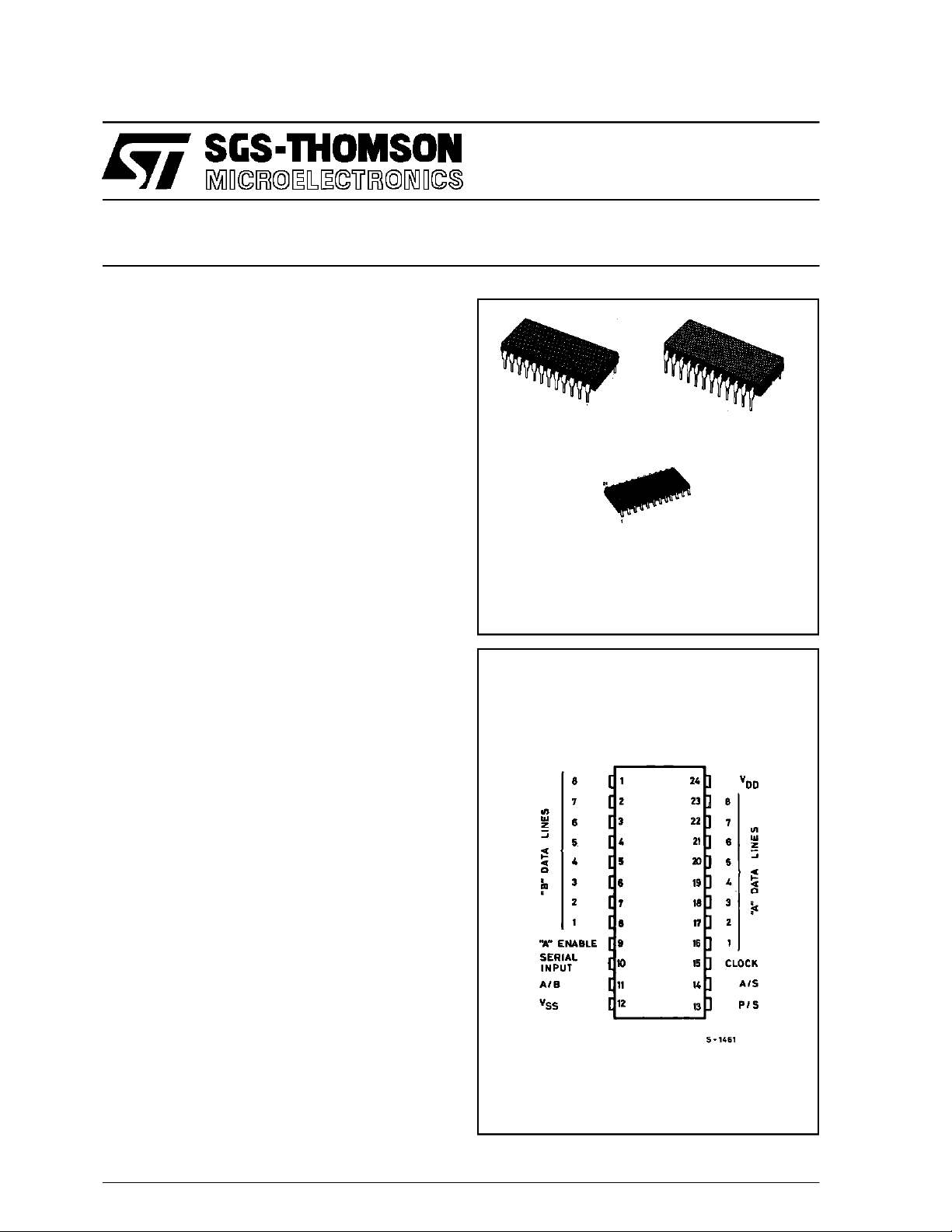
HCC/HCF4034B
INPUT/OUTPUT BUS REGISTER
EY
(Plastic Package)
HCC4034BF HCF4034BEY
PIN CO N NECTIONS
(Ceramic Frit Seal Package)
M1
(MicroPackage)
ORDER CODES :
HCF4034BM1
F
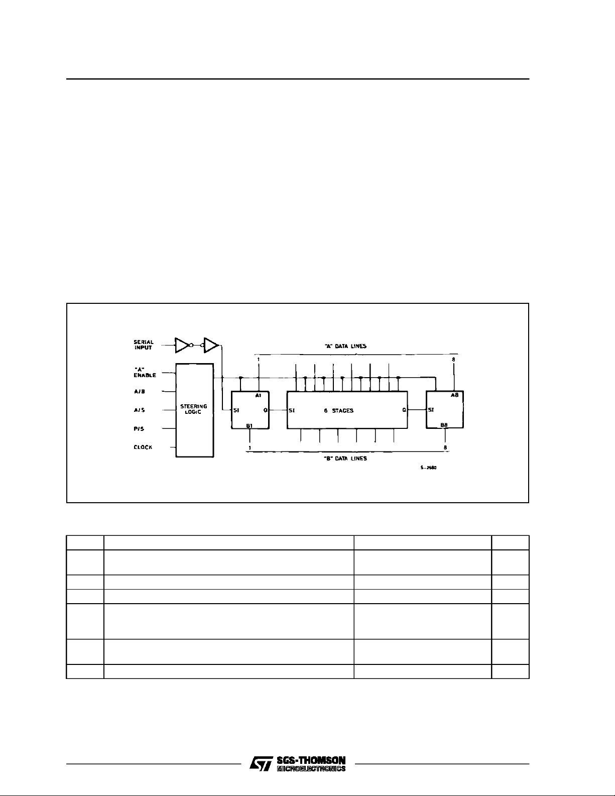
DESCRIPTION
TheHCC4034B(extended temperature range) and
HCF4034B (intermediate temperature range) are
monolithic integrated circuits, available in 24-lead
dual in-line plastic or ceramic package and plastic
micro package. The HCC/HCF4034B is a static
eight-stage parallel-or serial-input parallel-output
register. Itcan be used to : 1) bidirectionally transfer
parallel information between two buses ; 2) convert
serial data to parallel form and direct the parallel
datatoeitheroftwobuses ;3)store(recirculate)paralleldata,or4)acceptparallel datafromeitheroftwo
buses and convert that data to serial form. Inputs
that control the operations include a single-phase
CLOCK (CL), A DATA ENABLE (AE), ASYNCHRONOUS/SYNCHRONOUS(A/S), A-BUS-TOB-BUS/B-BUS-TO-A-BUS (A/B), and PARALLEL/
SERIAL (P/S). Data inputs include 16 bidirectional
parallel data lines of whichtheeightAdata linesare
inputs(3-stateoutputs) and the Bdatalinesare outputs (inputs) depending on the signal level on the
A/B input.In addition, an input for SERIAL DATAis
alsoprovided. AllregisterstagesareD-typemasterslaveflip-flops withseparatemasterandslaveclock
June 1989
1/16
HCC/HCF4034B
inputs generated internally toallowsynchronous or
asynchronous data transfer from master to slave.
Isolationfrom externalnoise andthe effectsofloading isprovidedby outputbuffering.
PARALLELOPERATION – A high P/S input signal
allowsdata transfer intothe register via theparallel
data lines synchronously with thepositive transition
of the clockprovided the A/S input islow. If the A/S
inputishigh thetransfer is independent oftheclock.
The direction of data flow is controlled by the A/B
input. When this signal ishigh the A data lines are
inputs (andB data linesare outputs); alowA/Bsignal reverses thedirection ofdata flow.The AE-input
is an additional feature which allowsmanyregisters
tofeeddatatoacommonbus.TheADATAlinesare
FUNCTIONAL DIAGRAM
enabledonly whenthis signal is high. Datastorage
through recirculation of data in each register stage
is accomplished by making theA/B signalhigh and
the AE signallow.
SERIALOPERATION –AlowP/Ssignal allowsserial data to transfer into the register synchronously
withthe positivetransitionoftheclock.TheA/Sinput
isinternally disabledwhenthe register isin theserial
mode (asynchronous serial operation is not
allowed). The serial dataappears asoutputdataon
either the B lines (when A/B is high) or the A lines
(whenA/B islowandtheAEsignal ishigh).Register
expansion can beaccomplished by simply cascading HCC/HCF4034B packages.
ABSOLUTE MAXIMUM RATINGS
Symbol Parameter Value Unit
* Supply Voltage : HCC Types
V
DD
V
Input Voltage – 0.5 to VDD+ 0.5 V
i
I
DC Input Current (any one input) ± 10 mA
I
P
T
T
Stresses above those listed under ”Absolute Maximum Ratings” may cause permanent damage to the device. This is a stress
rating only and functional operation of the device at these or any other conditions above those indicated in the operational sections of this specification is not implied. Exposure to absolute maximum rating conditions for external periods may affect device
reliability.
2/16
Total Power Dissipation (per package)
tot
Dissipation per Output Transistor
for T
= Full Package-temperature Range
op
Operating Temperature : HCC Types
op
Storage Temperature – 65 to + 150 °C
stg
HCF Types
HCF Types
– 0.5 to + 20
– 0.5 to + 18
200
100
– 55 to + 125
–40to+85
V
V
mW
mW
°C
°C
HCC/HCF4034B
RECOMMENDED OPERATINGCONDITIONS
Symbol Parameter Value Unit
V
T
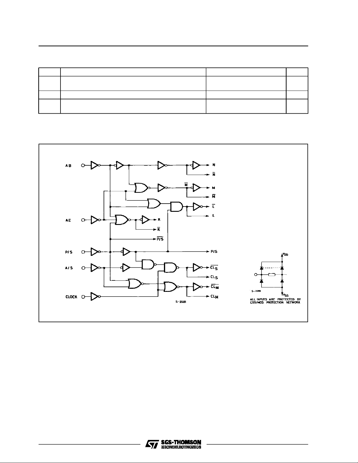
LOGIC DIAGRAMS
STEERING LOGIC
Supply Voltage : HCC Types
DD
HCF Types
V
Input Voltage 0 to V
I
Operating Temperature : HCC Types
op
HCF Types
3to18
3to15
DD
– 55 to + 125
–40to+85
V
V
V
°C
°C
3/16
HCC/HCF4034B
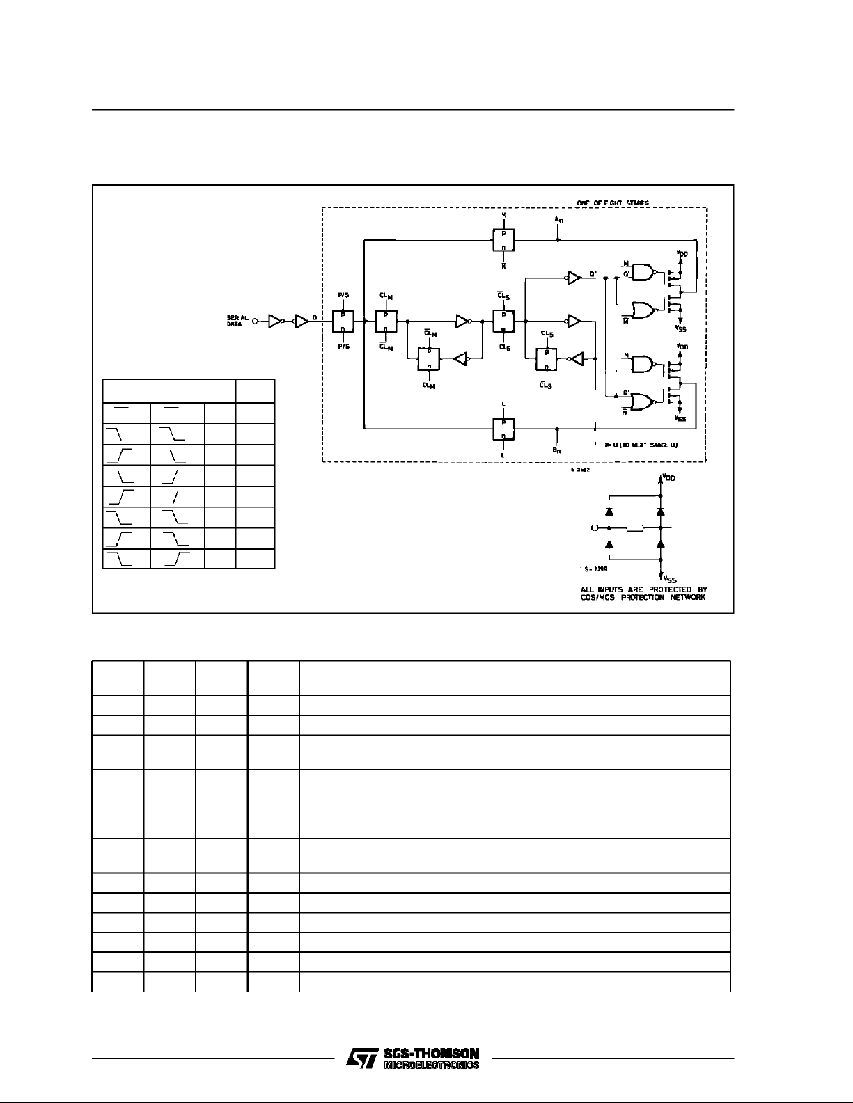
LOGIC DIAGRAM AND TRUTH TABLE
REGISTER STAGE (1 of 8 stages)
INPUTS OUT
▲
CL
M
▲ = LEVEL CHANGE
• = INVALID CONDI-
CL
▲
S
DQ
00
00
0•
X0
11
11
1•
FOR REGISTER INPUT-LEVELSAND RESULTING REGISTER OPERATION
”A”
Enable
0 0 0 X Serial Mode ; Synch. Serial Data Input, ”A” Parallel Data Outputs Disabled
0 0 1 X Serial Mode ; Synch. Serial Data Input, ”B” Parallel Data Output
0 1 0 0 Parallel Mode ; ”B” Synch. Parallel Data Inputs, ”A” Parallel Data Outputs
0 1 0 1 Parallel Mode ; ”B” Asynch. Parallel Data Inputs, ”A” Parallel Data Outputs
0 1 1 0 Parallel Mode ; ”A” Parallel Data Inputs Disabled, ”B” Parallel Data Outputs,
0 1 1 1 Parallel Mode ; ”A” Parallel Data Inputs Disabled, ”B” Parallel Data Outputs,
1 0 0 X Serial Mode ; Synch. Serial Data Input, ”A” Parallel Data Output
1 0 1 X Serial Mode ; Synch. Serial Data Input, ”B” Parallel Data Output
1 1 0 0 Parallel Mode ; ”B” Synch. Parallel Data Input, ”A” Parallel Data Output
1 1 0 1 Parallel Mode ; ”B” Asynch. Parallel Data Input, ”A” Parallel Data Output
1 1 1 0 Parallel Mode ; ”A” Synch. Parallel Data Input, ”B” Parallel Data Output
1 1 1 1 Parallel Mode ; ”A” Asynch. Parallel Data Input, ”B” Parallel Data Outpu
* Outputs change at positive transition of clock in the serial mode and when the A/S control inputs is ”low” in the parallel
mode.
4/16
P/S A/B A/S Operation*
Disabled
Disabled
Synch. Data Recirculation
Asynch. Data Recirculation
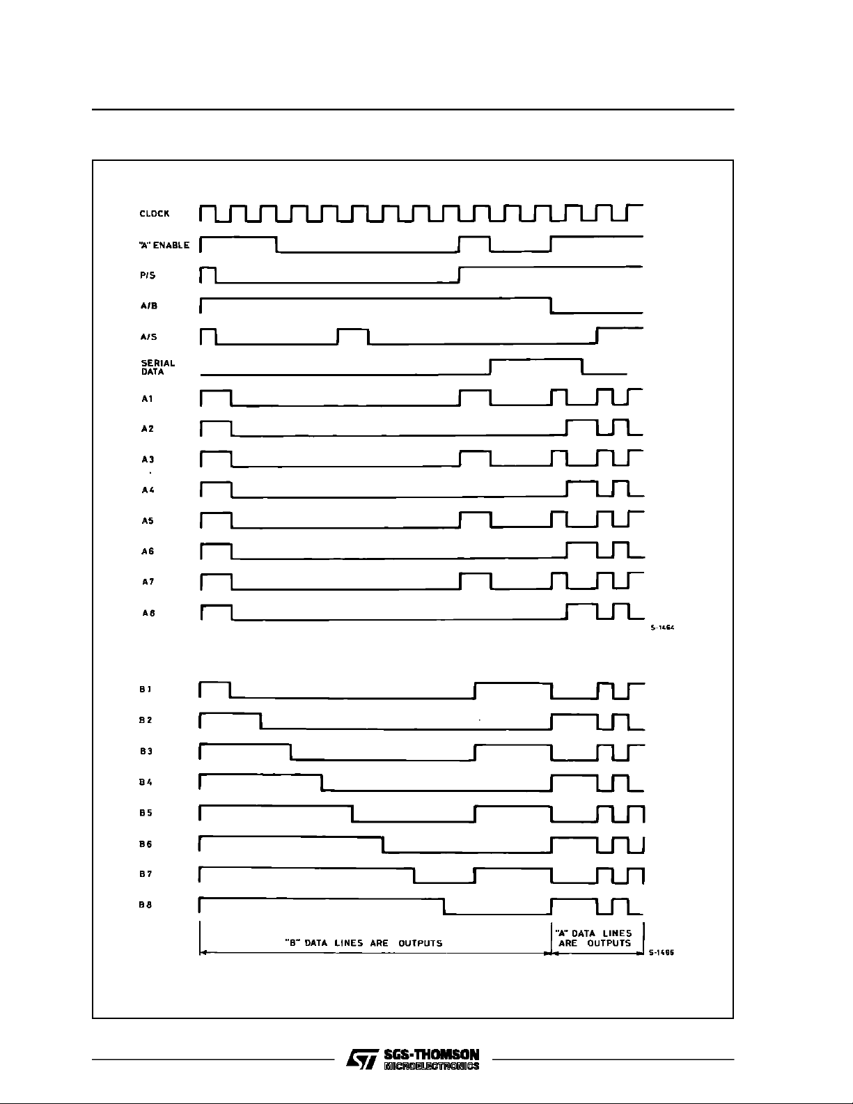
TIMING DIAGRAM
HCC/HCF4034B
5/16
HCC/HCF4034B
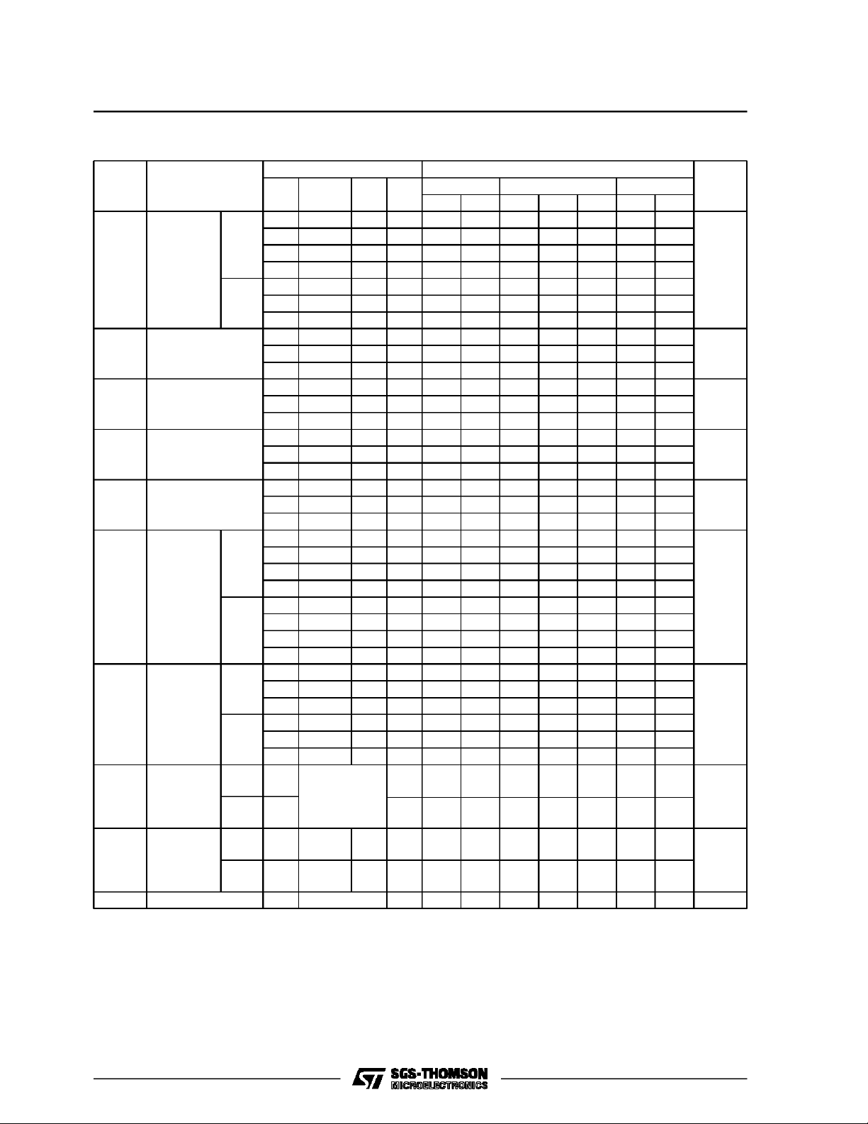
STATIC ELECTRICAL CHARACTERISTICS (over recommendedoperating conditions)
Test Conditions Values
Symbol Parameter
(V) (V) (µA) (V)
I
L
Quiescent
Current
HCC
Types
0/ 5 5 5 0.04 5 150
0/10 10 10 0.04 10 300
0/15 15 20 0.04 20 600
0/20 20 100 0.08 100 3000
HCF
Types
OH
Output High
V
Voltage
0/ 5 5 20 0.04 20 150
0/10 10 40 0.04 40 300
0/15 15 80 0.04 80 600
0/ 5 < 1 5 4.95 4.95 4.95
0/10 < 1 10 9.95 9.95 9.95
0/15 < 1 15 14.95 14.95 14.95
OL
Output Low
V
Voltage
5/0 < 1 5 0.05 0.05 0.05
10/0 < 1 10 0.05 0.05 0.05
15/0 < 1 15 0.05 0.05 0.05
IH
Input High
V
Voltage
IL
Input Low
V
Voltage
OH
Output
Drive
Current
HCC
Types
I
0/ 5 2.5 5 – 2 – 1.6 – 3.2 – 1.15
0/ 5 4.6 5 – 0.64 – 0.51 – 1 – 0.36
0/10 9.5 10 – 1.6 – 1.3 – 2.6 – 0.9
0/15 13.5 15 – 4.2 – 3.4 – 6.8 – 2.4
0/ 5 2.5 5 – 1.53 – 1.36 – 3.2 – 1.1
HCF
Types
0/ 5 4.6 5 – 0.52 – 0.44 – 1 – 0.36
0/10 9.5 10 – 1.3 – 1.1 – 2.6 – 0.9
0/15 13.5 15 – 3.6 – 3.0 – 6.8 – 2.4
OL
Output
Sink
Current
HCC
Types
I
HCF
Types
I
IH,IIL
Input
Leakage
Current
HCC
Types
HCF
Types
I
OH
3-State
Output
Leakage
Current
Input Capacitance Any Input 5 7.5 pF
C
I
*T
=–55°CforHCC device : – 40°C for HCF device.
Low
*T
= + 125°CforHCC device : + 85°CforHCF device.
High
TheNoise Margin for both”1” and ”0” levelis : 1V min.with VDD= 5V, 2V min. with VDD= 10V, 2.5V min.with VDD= 15V.
HCC
Types
HCF
Types
0/ 5 0.4 5 0.64 0.51 1 0.36
0/10 0.5 10 1.6 1.3 2.6 0.9
0/15 1.5 15 4.2 3.4 6.8 2.4
0/ 5 0.4 5 0.52 0.44 1 0.36
0/10 0.5 10 1.3 1.1 2.6 0.9
0/15 1.5 15 3.6 3.0 6.8 2.4
0/18
0/15
0/18 0/18 18 ± 0.4 ±10
0/15 0/15 15 ± 1.0 ±10
V
V
I
O
|IO|V
DD
T
* 25°CT
Low
Min. Max. Min. Typ. Max. Min. Max.
0.5/4.5 < 1 5 3.5 3.5 3.5
1/9 < 1 10 7 7 7
1.5/13.5 < 1 15 11 11 11
4.5/0.5 < 1 5 1.5 1.5 1.5
9/1 < 1 10 3 3 3
13.5/1.5 < 1 15 4 4 4
18 ± 0.1 ±10
Any Input
15 ± 0.3 ±10
–5
± 0.1 ± 1
–5
± 0.3 ± 1
–4
± 0.4 ± 12
–4
± 1.0 ± 7.5
High
Unit
*
µA
V
V
V
V
mA
mA
µA
µA
6/16

HCC/HCF4034B
DYNAMIC ELECTRICAL CHARACTERISTICS(T
=25°C, CL= 50pF, RL= 200kΩ,
amb
typical temperature coefficient for all VDDvalues is 0.3%/°C, all input rise and fall times = 20ns)
Symbol Parameter
t
PHL,tPLH
Propagation Delay Time :
A (B) Parallel Data in to
B (A) Parallel Data Out
t
PLZ,tPHZ
t
PZL,tPZH
t
THL,tTLH
t
setup
3-state Propagation Delay Time
A/B or AE to ”A” OUT
Transition Time 5 100 200
Data Setup Time Serial Data to
Clock
Parallel Data to Clock 5 25 50
t
w
High-level Pulse Width, AE, P/S,
A/S
f
CL
t
W
t
r,tf
* If morethan one unit is cascaded. trshouldbe madeless than orequal to the sum of thetransition timeand the fixedpropagation delay ofthe
output ofthe drivingstage fortheestimated capacitive load.
Maximum Clock Frequency 5 2 4
Clock Pulse Width 5 125 250
* Clock Input Rise or Fall Time 5,10,15 15 µs
Test Conditions Value
V
(V) Min. Typ. Max.
DD
5 350 700
10 120 240
15 85 170
5 200 400
10 80 160
15 60 120
10 50 100
15 40 80
5 80 160
10 30 60
15 20 40
10 15 30
15 10 20
5 175 350
10 70 140
15 40 80
10 5 10
15 7 14
10 50 100
15 35 70
Unit
ns
ns
ns
ns
ns
ns
MHz
ns
7/16

HCC/HCF4034B
TypicalOutputLow (sink)Current Characteristics. Minimum Output Low (sink) Current Charac-
teristics.
Typical Output High (source) Current Characteristics.
Minimum Output High (source) Current Characteristics.
TYPICAL APPLICATIONS
16-BITPARALLEL IN/PARALLEL OUTPARALLEL IN/SERIAL OUT, SERIAL IN/PARALLEL OUT,SERIAL
IN/SERIALOUT REGISTER.
8/16

TYPICAL APPLICATIONS (continued)
16-BITSERIALIN/GATED PARALLEL OUT REGISTER
FREQUENCYAND PHASECOMPARATOR.
HCC/HCF4034B
TIMINGDIAGRAM
9/16

HCC/HCF4034B
TYPICAL APPLICATIONS (continued)
SHIFTRIGHT/SHIFTLEFT WITH PARALLEL INPUTS
A ”High” (”Low”) on the Shift Left/Shift Right input
allowsserial data on the Shift Left Input (Shift Right
Input) to enterthe register onthe positive transition
of the clocksignal. A ”high” onthe ”A” Enable Input
disables the”A” parallel data lines on Reg.1 and 2
and enables the ”A” datalines on registers 3 and4
and allowsparallel dataintoregisters 1and 2. Other
logic schemes may be used in place of registers 3
and 4 forparallel loading. When parallel inputs are
not used Reg. 3 and 4 and associatedlogic arenot
required.
* ShiftLeft input mustbe disabled during parallel
entry.
N-STAGEREGISTER WITH FIXEDSERIAL OUTPUT LINE
10/16

TYPICAL APPLICATIONS (continued)
SAMPLEAND HOLDREGISTER-SERIAL/PARALLEL IN-PARALLEL OUT
SINGLE-AND DOUBLE-BUSSYSTEMS
HCC/HCF4034B
The ”A” enable (AE) and A/B signals control all combinations of transfer between the registers and bus systems.
11/16

HCC/HCF4034B
TEST CIRCUITS
QuiescentDevice Current.
Input Leakage Current.
Noise Immunity.
12/16

Plastic DIP24 (0.25) MECHANICAL DATA
HCC/HCF4034B
DIM.
MIN. TYP. MAX. MIN. TYP. MAX.
a1 0.63 0.025
b 0.45 0.018
b1 0.23 0.31 0.009 0.012
b2 1.27 0.050
D 32.2 1.268
E 15.2 16.68 0.598 0.657
e 2.54 0.100
e3 27.94 1.100
F 14.1 0.555
I 4.445 0.175
L 3.3 0.130
mm inch
P043A
13/16

HCC/HCF4034B
Ceramic DIP24 MECHANICAL DATA
DIM.
MIN. TYP. MAX. MIN. TYP. MAX.
A 32.3 1.272
B 13.05 13.36 0.514 0.526
C 3.9 5.08 0.154 0.200
D 3 0.118
E 0.5 1.78 0.020 0.070
e3 27.94 1.100
F 2.29 2.79 0.090 0.110
G 0.4 0.55 0.016 0.022
I 1.17 1.52 0.046 0.060
L 0.22 0.31 0.009 0.012
M 1.52 2.49 0.060 0.098
N1
P 15.4 15.8 0.606 0.622
Q 5.71 0.225
4° (min.), 15° (max.)
mm inch
14/16
P058C

SO24 MECHANICAL DATA
HCC/HCF4034B
DIM.
MIN. TYP. MAX. MIN. TYP. MAX.
A 2.65 0.104
a1 0.10 0.20 0.004 0.007
a2 2.45 0.096
b 0.35 0.49 0.013 0.019
b1 0.23 0.32 0.009 0.012
C 0.50 0.020
c1 45° (typ.)
D 15.20 15.60 0.598 0.614
E 10.00 10.65 0.393 0.420
e 1.27 0.05
e3 13.97 0.55
F 7.40 7.60 0.291 0.299
L 0.50 1.27 0.19 0.050
S8°(max.)
mm inch
L
A
a2
b
e3
D
24 13
112
e
F
s
a1
c1
b1
C
E
15/16

HCC/HCF4034B
Information furnished is believed tobe accurate and reliable.However, SGS-THOMSON Microelectronicsassumes no responsability forthe
consequences of useof such information nor for any infringement of patents orother rights of third parties which may results fromits use. No
license isgranted byimplication or otherwiseunder any patentorpatent rights ofSGS-THOMSON Microelectronics. Specificationsmentioned
in this publication are subject to changewithout notice. This publication supersedes andreplaces all information previously supplied.
SGS-THOMSON Microelectronicsproductsare notauthorized foruse ascritical componentsinlife support devicesor systems withoutexpress
written approval of SGS-THOMSONMicroelectonics.
1994 SGS-THOMSON Microelectronics - All RightsReserved
Australia - Brazil - France - Germany- HongKong - Italy - Japan - Korea- Malaysia - Malta -Morocco - The Netherlands-
Singapore - Spain - Sweden - Switzerland - Taiwan - Thailand - UnitedKingdom - U.S.A
SGS-THOMSON Microelectronics GROUP OF COMPANIES
16/16

WWW.ALLDATASHEET.COM
Copyright © Each Manufacturing Company.
All Datasheets cannot be modified without permission.
This datasheet has been download from :
www.AllDataSheet.com
100% Free DataSheet Search Site.
Free Download.
No Register.
Fast Search System.
www.AllDataSheet.com
 Loading...