

查询HCC/HCF40192B供应商
PRESETTABLE UP/DOWN COUNTERS (DUAL CLOCK
WITH RESET) 40192B – BCD TYPE40193B – BINARY TYPE
.INDIVIDUAL CLOCK LINES FOR COUNTING
UP ORCOUNTINGDOWN
.SYNCHRONOUS HIGH-SPEED CARRY AND
BORROWPROPAGATIONDELAYSFORCASCADING
.ASYNCHRONOUS RESETAND PRESET CA-
PABILITY
.MEDIUM-SPEED OPERATION - f
(typ.)@ 10V
CL
.STANDARDIZED SYMMETRICAL OUTPUT
CHARACTERISTICS
.5V, 10V, AND 15V PARAMETRIC RATINGS
.INPUT CURRENTOF100nA AT 18V AND25°C
FOR HCC DEVICE
.100% TESTEDFOR QUIESCENTCURRENT
.MEETSALLREQUIREMENTSOFJEDECTEN-
TATIVESTANDARDN°13A,”STANDARD SPECIFICATIONS FOR DESCRIPTION OF ”B”
SERIESCMOS DEVICES”
= 8MHz
HCC/HCF40192B
HCC/H CF4 01 93B
EY
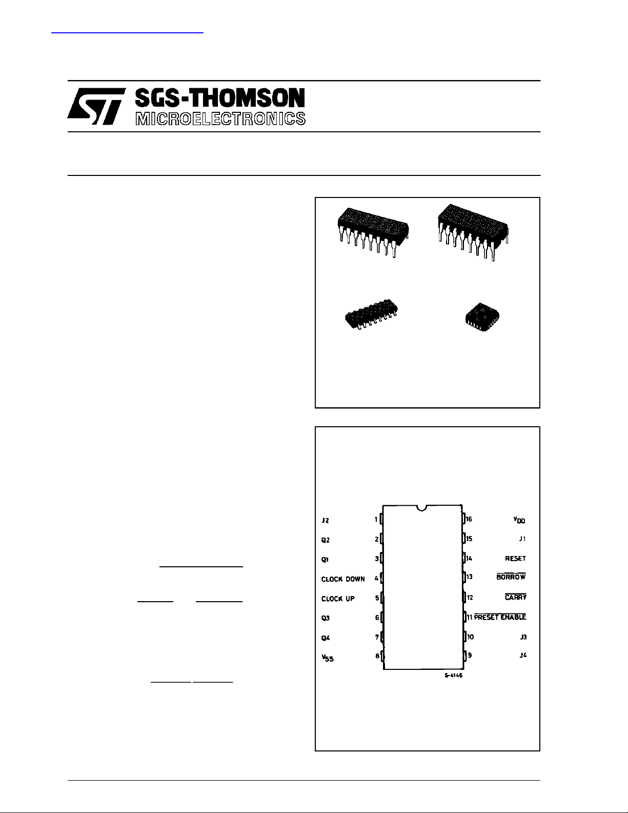
(Plastic Package)F(Ceramic Frit Seal Package)
M1
(Chip Carrier)
ORDER CODES :
HCC401XXBF HCF401XXBM1
HCF401XXBEY HCF401XXBC1
(Plastic Chip Carrier)
C1
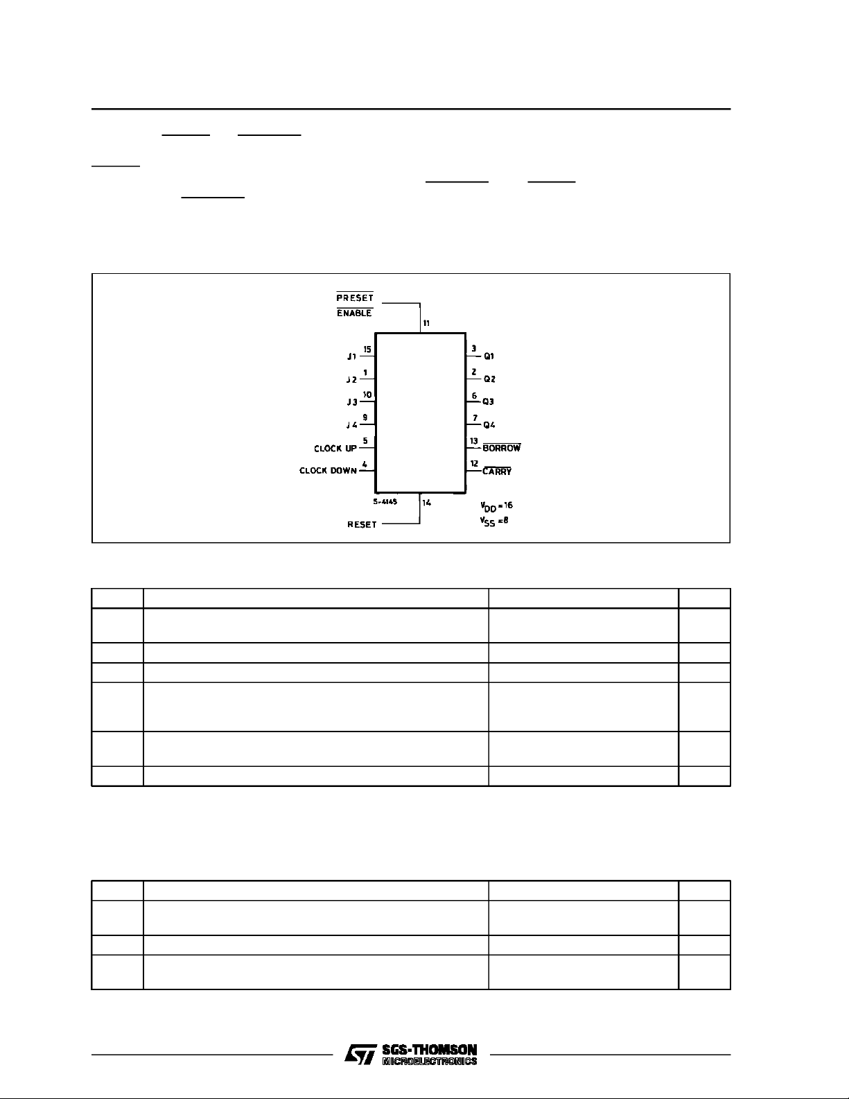
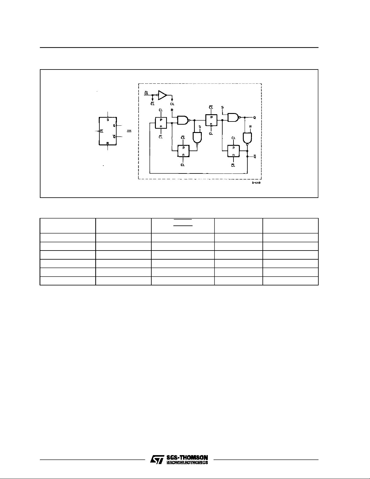
DESCRIPTI ON
The HCC40192B, HCC40193B, (extended tem-
peraturerange) and the HCF40192B, HCF40193B
(intermediate temperature range) are monolithic integrated circuits, available in 16-lead dual in-line
plastic or ceramic package and platic micro package. The HCC/HCF40192B Presettable BCD
Up/DownCounter and theHCC/HCF40193B Pres-
ettable BinaryUp/Down Counter each consist of 4
synchronously clocked, gated ”D” type flip-flops
connected as a counter. The inputs consist of 4 individual jam lines,a PRESET ENABLE control, individual CLOCK UP and CLOCK DOWN signals
and a master RESET. Four buffered Q signal outputs as well as CARRY and BORROW outputs for
multiple-stage counting schemesareprovided. The
counter is cleared so that all outputs are in a low
stateby a high on the RESET line. A RESET isaccomplished asynchronously with the clock. Each
output is individually programmable asynchronouslywith theclocktothelevelonthecorresponding
jaminputwhenthePRESETENABLEcontrol islow.
The counter counts up one count on the positive
clock edge of the CLOCK UP signal provided the
CLOCK DOWN line is high. The counter counts
down one count on the positive clock edge of the
CLOCKDOWN signal provided the CLOCK UP line
PIN CONNECTIONS
June1989
1/15
HCC/HCF40192B/193B
is high.TheCARRYandBORROWsignals arehigh
when the counter is counting up or down. The
CARRY signal goes low one-half clock cycle after
thecounterreaches itsmaximumcountinthecountup mode. The BORROW signal goes low one-half
clock cycle after the counter reaches its minimum
FUN CTIONAL DIAG R A M
count in the count-down mode. Cascading of
multiple packages is easily accomplished without
the need foradditional externalcircuitrybytying the
BORROW and CARRY outputs to the CLOCK
DOWN and CLOCK UP inputs, respectively, of the
succeeding package.
ABSOLUTE MAXIMUM RATIN GS
Symbol Parameter Value Unit
V
* Supply Voltage :HC C Types
DD
HCF Types
V
Input Voltage – 0.5 to VDD+ 0.5 V
i
I
DC Input Current (any one input) ± 10 mA
I
P
Total Power Dissipation (per package)
tot
– 0.5 to + 20
– 0.5 to + 18
200
V
V
mW
Dissipation per Output Transistor
for Top= Full Package-temperature Range
T
Operating Temperature : HCC Types
op
HCF Types
T
Stresses above those listed under ”Absolute Maximum Ratings” may cause permanent damage to the device. This is a stress
rating only and functional operation of the device at these or any other conditions above those indicated in the operational sections
of this specification is not implied. Exposure to absolute maximum rating conditions for external periods may affect device reliability.
* All voltages are with respect to VSS(GND).
Storage Temperature – 65 to + 150 °C
stg
100
– 55 to + 125
–40to+85
mW
°C
°C
RECOMMENDED OPERATING CO NDITIONS
Symbol Parameter Value Unit
V
T
Supply Voltage : HCC Types
DD
HCF Types
V
Input Voltage 0 to V
I
Operating Temperature : HCC Types
op
HCF Types
3to18
3to15
DD
– 55 to + 125
–40to+85
V
V
V
°C
°C
2/15
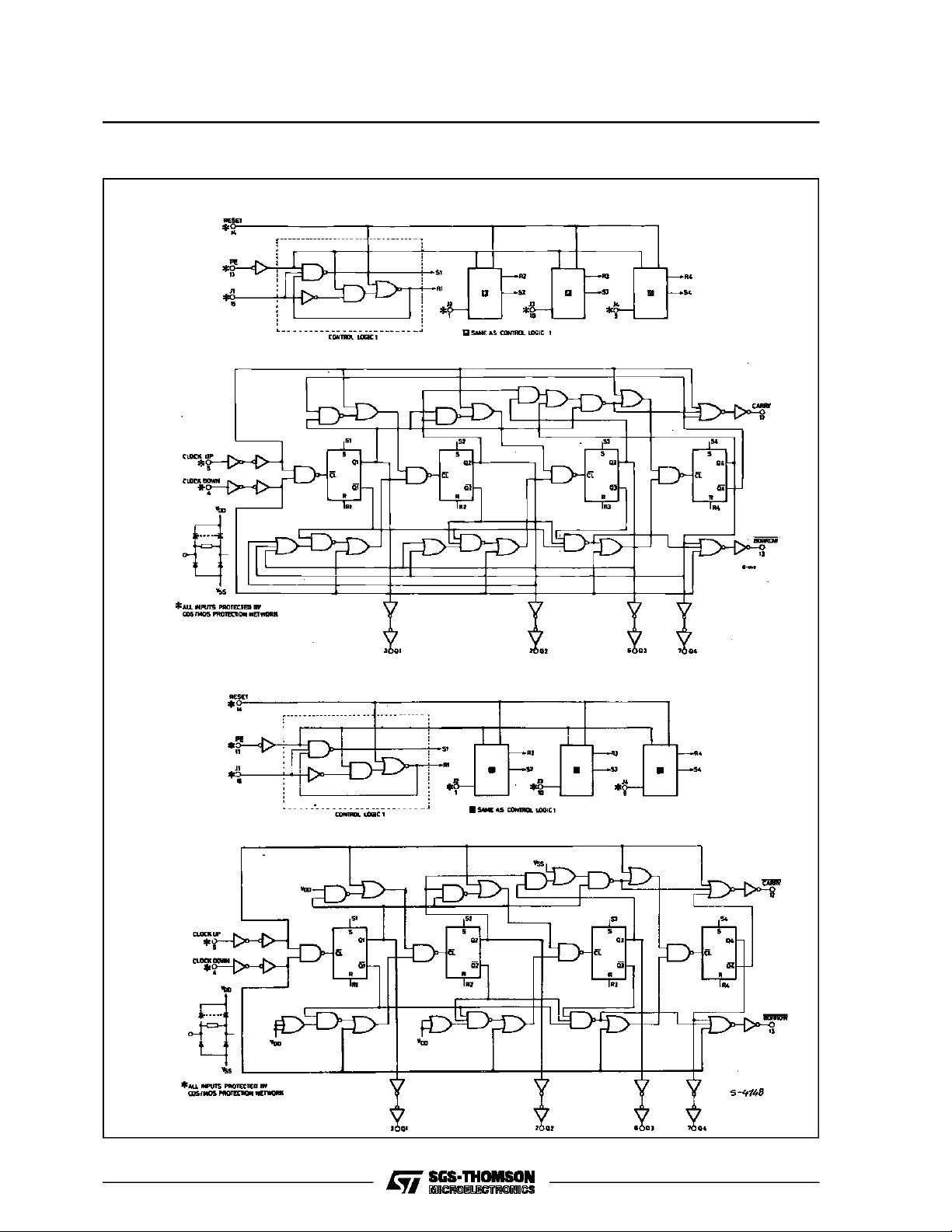
LOGI C DI AGRAMS
40192B (BCD).
HCC/HCF40192B/193B
40193B (Binary).
3/15
HCC/HCF40192B/193B
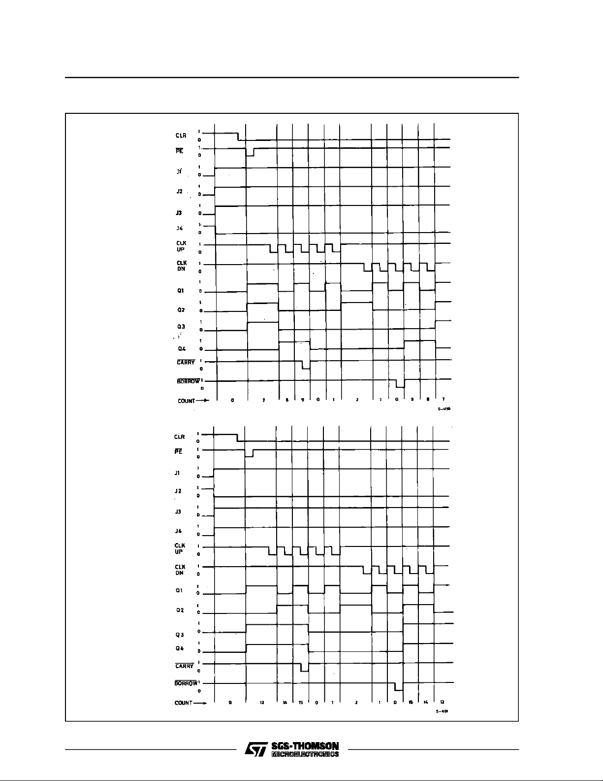
TIM ING D IAG R AMS
40192B (BCD).
40193B (Binary).
4/15
InternalLogic of Flip-flop.
TRUTH TABLE
HCC/HCF40192B/193B
Clock
Up
–
/
–
–
\
–
1
1
X X 0 0 Preset
X X X 1 Reset
1 = High Level 0 = Low Level X = Don’t Care.
Clock
Down
1 1 0 Count Up
1 1 0 No Count
–
/
–
–
\
–
Pres et
Enab l e
1 0 Count Down
1 0 No Count
Reset Action
5/15

HCC/HCF40192B/193B
STATIC ELECTRICAL CHARACTERISTICS(over recommended operating conditions)
Test Conditions Valu e
Symbol P arameter
Quiescent
I
L
Current
HCC
Types
HCF
Types
V
OH
Output High
Voltage
V
OL
Output Low
Voltage
V
IH
Input High
Voltage
V
IL
Input Low
Voltage
I
OH
Output
Drive
Current
HCC
Types
HCF
Types
I
OL
Output
Sink
Current
HCC
Types
HCF
Types
I
IH,IIL
Input
Leakage
Current
HCC
Types
HCF
Types
C
Input Capacitance Any Input 5 7.5 pF
I
*T
=–55°CforHCC device : – 40°CforHCF device.
Low
*T
= + 125°CforHCC device : + 85°CforHCF device.
High
The Noise Margin for both ”1” and ”0” level is : 1V min. with VDD= 5V, 2V min. with VDD= 10V, 2.5V min. with VDD=
V
V
O
|IO|V
I
(V) (V) (µA) (V)
T
DD
* 25°CT
Low
Min. M ax. Min. Typ. Ma x. Min. Max.
High
*
0/ 5 5 5 0.04 5 150
0/10 10 10 0.04 10 300
0/15 15 20 0.04 20 600
0/20 20 100 0.08 100 3000
0/ 5 5 20 0.04 20 150
0/10 10 40 0.04 40 300
0/15 15 80 0.04 80 600
0/ 5 < 1 5 4.95 4.95 4.95
0/10 < 1 10 9.95 9.95 9.95
0/15 < 1 15 14.95 14.95 14.95
5/0 < 1 5 0.05 0.05 0.05
10/0 < 1 10 0.05 0.05 0.05
15/0 < 1 15 0.05 0.05 0.05
0.5/4.5 < 1 5 3.5 3.5 3.5
1/9 < 1 10 7 7 7
1.5/13.5 < 1 15 11 11 11
4.5/0.5 < 1 5 1.5 1.5 1.5
9/1 < 1 10 3 3 3
13.5/1.5 < 1 15 4 4 4
0/ 5 2.5 5 – 2 – 1.6 – 3.2 – 1.15
0/ 5 4.6 5 – 0.64 – 0.51 – 1 – 0.36
0/10 9.5 10 – 1.6 – 1.3 – 2.6 – 0.9
0/15 13.5 15 – 4.2 – 3.4 – 6.8 – 2.4
0/ 5 2.5 5 – 1.53 – 1.36 – 3.2 – 1.1
0/ 5 4.6 5 – 0.52 – 0.44 – 1 – 0.36
0/10 9.5 10 – 1.3 – 1.1 – 2.6 – 0.9
0/15 13.5 15 – 3.6 – 3.0 – 6.8 – 2.4
0/ 5 0.4 5 0.64 0.51 1 0.36
0/10 0.5 10 1.6 1.3 2.6 0.9
0/15 1.5 15 4.2 3.4 6.8 2.4
0/ 5 0.4 5 0.52 0.44 1 0.36
0/10 0.5 10 1.3 1.1 2.6 0.9
0/15 1.5 15 3.6 3.0 6.8 2.4
0/18
18 ± 0.1 ±10
–5
± 0.1 ± 1
Any Input
0/15
15 ± 0.3 ±10
–5
± 0.3 ± 1
Unit
µA
V
V
V
V
mA
mA
µA
6/15

HCC/HCF40192B/193B
DYNAMIC ELECTRICAL CHARACTERISTICS (T
=25°C, CL= 50pF, RL= 200kΩ,
amb
typical temperature coefficient for all VDDvalues is 0.3%/°C, all input rise and fall time = 20ns)
Symbol Parameter
t
,
PHL
t
PLH
Propagation Delay Time
Clock Up or Clock Down to Q
Reset to Q
PE to Q 5 200 400
Clock Up to Carry
Clock Down to Borrow
Reset or PR to Borrow or Carry 5 300 600
t
,
Transition Time 5 100 200
* Removal Time
t
t
THL
TLH
re m
Reset or PE
t
Clock Input Pulse Width
W
Reset
PE 5 120 240
Clock 5 90 180
t
r,tf
f
CL
* The time required for Reset or Preset Enable control to be removed before clocking (see timing diagram).
Clock Input Rise or Fall Time 5 15
Maximum Clock Input Frequency 5 2 4
Test Conditions Value
(V) Min. Typ . Max.
V
DD
5250500
10 120 240
15 90 180
10 100 200
15 70 140
5160320
10 80 160
15 60 120
10 150 300
15 110 220
10 50 100
15 40 80
58040
10 40 20
15 30 15
5 480 240
10 300 150
15 260 130
10 85 170
15 70 140
10 45 90
15 30 60
10 15
15 5
10 5 8
15 5.5 11
Unit
ns
ns
ns
ns
ns
ns
ns
ns
ns
µs
MHz
7/15

HCC/HCF40192B/193B
TimingDiagram Defining t
rem
.
OutputLow (sink) Current Characteristics. Outputhigh (source) Current Characteristics.
TypicalTransitionTime vs. Load Capacitance. Typical Propagation Delay Time vs. Load Capacit-
ance.
8/15
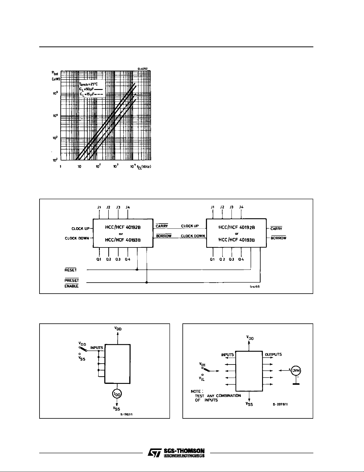
TypicalDynamicPower Dissipation.
TYPICAL APPLICA TI O N
CASCADED COUNTER PACKAGES
HCC/HCF40192B/193B
TEST CIRCUITS
QuiescentDevice Current. Input Voltage.
9/15

HCC/HCF40192B/193B
TEST CIRCUITS (c onti n ued)
Input Leakage Current. DynamicPower Dissipation.
10/15

HCC/HCF40192B/193B
Plastic DIP16 (0.25) MECHANICAL DATA
DIM.
MIN. TYP. MAX. MIN. TYP. MAX.
a1 0.51 0.020
B 0.77 1.65 0.030 0.065
b 0.5 0.020
b1 0.25 0.010
D 20 0.787
E 8.5 0.335
e 2.54 0.100
e3 17.78 0.700
F 7.1 0.280
I 5.1 0.201
L 3.3 0.130
Z 1.27 0.050
mm inch
P001C
11/15

HCC/HCF40192B/193B
Ceramic DIP16/1 MECHANICAL DATA
DIM.
MIN. TYP. MAX. MIN. TYP. MAX.
A 20 0.787
B 7 0.276
D 3.3 0.130
E 0.38 0.015
e3 17.78 0.700
F 2.29 2.79 0.090 0.110
G 0.4 0.55 0.016 0.022
H 1.17 1.52 0.046 0.060
L 0.22 0.31 0.009 0.012
M 0.51 1.27 0.020 0.050
N 10.3 0.406
P 7.8 8.05 0.307 0.317
Q 5.08 0.200
mm inch
12/15
P053D

SO16 (Narrow) MECHANICAL DATA
HCC/HCF40192B/193B
DIM.
MIN. TYP. MAX. MIN. TYP. MAX.
A 1.75 0.068
a1 0.1 0.2 0.004 0.007
a2 1.65 0.064
b 0.35 0.46 0.013 0.018
b1 0.19 0.25 0.007 0.010
C 0.5 0.019
c1 45° (typ.)
D 9.8 10 0.385 0.393
E 5.8 6.2 0.228 0.244
e 1.27 0.050
e3 8.89 0.350
F 3.8 4.0 0.149 0.157
G 4.6 5.3 0.181 0.208
L 0.5 1.27 0.019 0.050
M 0.62 0.024
S8°(max.)
mm inch
P013H
13/15

HCC/HCF40192B/193B
PLCC20 MECHANICAL DATA
DIM.
MIN. TYP. MAX. MIN. TYP. MAX.
A 9.78 10.03 0.385 0.395
B 8.89 9.04 0.350 0.356
D 4.2 4.57 0.165 0.180
d1 2.54 0.100
d2 0.56 0.022
E 7.37 8.38 0.290 0.330
e 1.27 0.050
e3 5.08 0.200
F 0.38 0.015
G 0.101 0.004
M 1.27 0.050
M1 1.14 0.045
mm inch
14/15
P027A

HCC/HCF40192B/193B
Information furnished isbelieved to be accurate and reliable. However, SGS-THOMSON Microelectronics assumes no responsability for the
consequences of use of suchinformation nor forany infringementof patents orother rights of third parties which mayresults from its use. No
license is granted by implication or otherwise underany patent or patent rights of SGS-THOMSON Microelectronics. Specificationsmentioned
in this publicationare subject to change without notice. This publication supersedes and replaces all information previously supplied.
SGS-THOMSON Microelectronicsproductsare notauthorized for use ascritical componentsinlife supportdevices orsystems withoutexpress
written approval of SGS-THOMSON Microelectonics.
1994SGS-THOMSON Microelectronics- All RightsReserved
Australia - Brazil - France - Germany - Hong Kong - Italy - Japan - Korea - Malaysia -Malta - Morocco - The Netherlands -
Singapore - Spain - Sweden - Switzerland - Taiwan -Thailand - United Kingdom - U.S.A
SGS-THOMSON Microelectronics GROUP OF COMPANIES
15/15
 Loading...