

查询HCC/HCF4008B供应商
4-BIT FULL ADDER WITH PARALLEL CARRY OUTPUT
.4 SUM OUTPUTS PLUS PARALLEL LOOK-
AHERDCARRY-OUTPUT
.HIGH-SPEED OPERATION-SUM IN-TO-SUM
OUT 160ns (typ.): CARRYIN-TO-CARRYOUT
50ns (typ.) AT VDD= 10V, CL= 50pF
.QUIESCENT CURRENT SPECIFIED TO 20V
FOR HCC DEVICE
.INPUT CURRENTOF 100nA AT 18VAND25°C
FOR HCC DEVICE
.100% TESTEDFOR QUIESCENTCURRENT
.5V, 10V,AND 15VPARAMETRIC RATING
.MEETSALLREQUIREMENTSOFJEDECTEN-
TATIVESTANDARDN°13A,”STANDARDSPECIFICATIONS FOR DESCRIPTION OF ”B”
SERIESCMOS DEVICES”
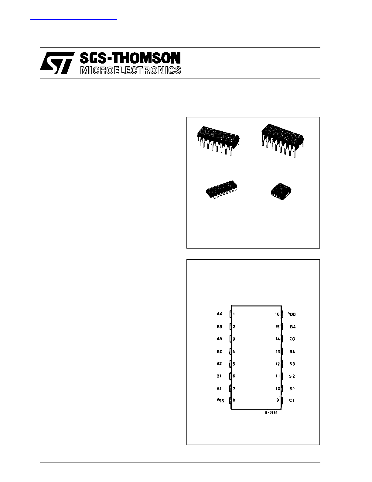
HCC/HCF4008B
EY
(Plastic Package)F(Ceramic Frit SealPackage)
M1
(MicroPackage)
ORDERCODES :
HCC4008BF HCF4008BM1
HCF4008BEY HCF4008BC1
(Plastic Chip Carrier)
C1
DESCRIPTION
TheHCC4008B (extended temperaturerange)and
HCF4008B (intermediate temperature range) are
monolithic integrated circuits, available in 16-lead
dual in-line plastic or ceramic package and plastic
micropackage.
TheHCC/HCF4008Btypesconsist offourfulladder
stages with fast look ahead carry provision from
stagetostage.Circuitry isincluded toprovidea fast
”parallel-carry-out” to permit high-speed operation
in arithmetic sections using several HCC/HCF
4008B’s.
HCC/HCF4008B inputsincludethe foursets of bits
tobe added,A1to A4andB1toB4, in addition to the
”Carry In” bit from a previous section.
HCC/HCF4008B outputs include the four sum bits,
S1toS4.Inaddition to thehighspeed”parallel-carryout” which may be utilized at a succeeding
HCC/HCF4008B section.
PIN CONNECTIONS
June1989
1/13
HCC/HCF4008B
ABSOLUTE MAX IMU M RATI NGS
Symbol Parameter Val ue Unit
V
* Supply Voltage : HCC Types
DD
HCF Types
V
Input Voltage – 0.5 to VDD+ 0.5 V
i
I
DC Input Current (any one input) ± 10 mA
I
P
Total Power Dissipation (per package)
tot
Dissipation per Output Transistor
for Top= Full Package-temperature Range
T
Operating Temperature : HCC Types
op
HCF Types
T
Stresses above those listed under ”Absolute Maximum Ratings” may cause permanent damage to the device. This is a stress
rating only and functional operation of the device at these or any other conditions above those indicated in the operational sections of this specification is not implied. Exposure to absolute maximum rating conditions for external periods may affect device
reliability.
* All voltage values are referred to VSSpin voltage.
Storage Temperature – 65 to + 150 °C
stg
RECOMMENDED OPERATING CONDITIONS
Symbol Parameter Value Unit
V
T
Supply Voltage : HCC Types
DD
HCF Types
V
Input Voltage 0 to V
I
Operating Temperature : HCC Types
op
HCF Types
– 0.5 to + 20
– 0.5 to + 18
200
100
–55to+125
–40to+85
3to18
3to15
DD
– 55 to + 125
–40to+85
V
V
mW
mW
°C
°C
V
V
V
°C
°C
2/13
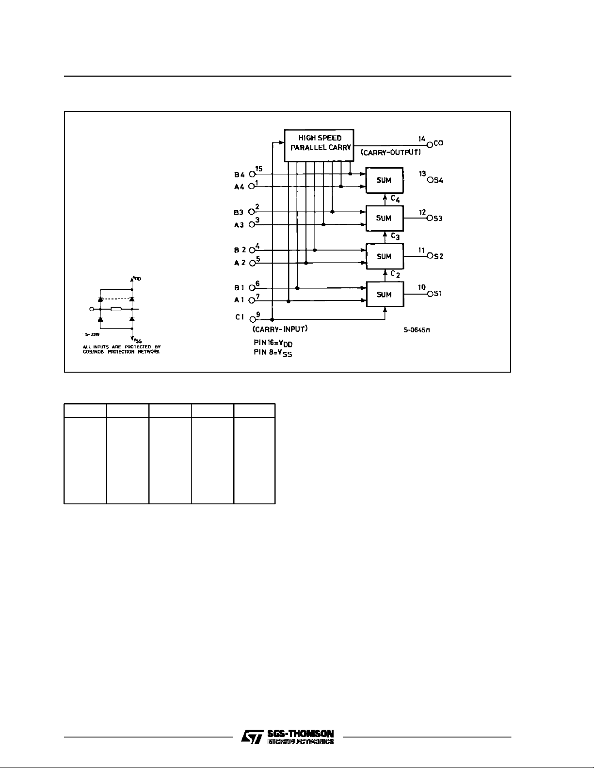
LOGIC DIAGRAM
HCC/HCF4008B
TRUTH TABLE
A
i
O
I
O
I
O
I
O
I
B
O
O
I
I
O
O
I
I
i
CI CO SUM
O
O
O
O
I
I
I
I
O
O
O
I
O
I
I
I
O
I
I
O
I
O
O
I
3/13
HCC/HCF4008B
STATIC EL ECTR ICA L CHARACTERISTICS (over recommended operating conditions)
Test Conditions Value
Symbol Parame te r
I
Quiescent
L
Current
HCC
Types
HCF
Types
V
OH
Output High
Voltage
V
OL
Output Low
Voltage
V
IH
Input High
Voltage
V
IL
Input Low
Voltage
I
OH
Output
Drive
Current
HCC
Types
HCF
Types
I
OL
Output
Sink
Current
HCC
Types
HCF
Types
I
IH,IIL
Input
Leakage
Current
HCC
Types
HCF
Types
C
Input Capacitance Any Input 5 7.5 pF
I
*T
=–55°CforHCC device : – 40°CforHCF device.
Low
*T
= + 125°CforHCC device : + 85°CforHCF device.
High
TheNoise Margin for both ”1” and ”0” level is : 1Vmin. with VDD= 5V, 2V min.with VDD=10V, 2.5 Vmin. withVDD= 15V.
V
V
O
|IO|V
I
(V) (V) (µA) (V)
T
DD
* 25°CT
Low
Min. Max. Min. Typ. M a x. Mi n. Max.
High
0/ 5 5 5 0.04 5 150
0/10 10 10 0.04 10 300
0/15 15 20 0.04 20 600
0/20 20 100 0.08 100 3000
0/ 5 5 20 0.04 20 150
0/10 10 40 0.04 40 300
0/15 15 80 0.04 80 600
0/ 5 < 1 5 4.95 4.95 4.95
0/10 < 1 10 9.95 9.95 9.95
0/15 < 1 15 14.95 14.95 14.95
5/0 < 1 5 0.05 0.05 0.05
10/0 < 1 10 0.05 0.05 0.05
15/0 < 1 15 0.05 0.05 0.05
0.5/4.5 < 1 5 3.5 3.5 3.5
1/9 < 1 10 7 7 7
1.5/13.5 < 1 15 11 11 11
4.5/0.5 < 1 5 1.5 1.5 1.5
9/1 < 1 10 3 3 3
13.5/1.5 < 1 15 4 4 4
0/ 5 2.5 5 – 2 – 1.6 – 3.2 – 1.15
0/ 5 4.6 5 – 0.64 – 0.51 – 1 – 0.36
0/10 9.5 10 – 1.6 – 1.3 – 2.6 – 0.9
0/15 13.5 15 – 4.2 – 3.4 – 6.8 – 2.4
0/ 5 2.5 5 – 1.53 – 1.36 – 3.2 – 1.1
0/ 5 4.6 5 – 0.52 – 0.44 – 1 – 0.36
0/10 9.5 10 – 1.3 – 1.1 – 2.6 – 0.9
0/15 13.5 15 – 3.6 – 3.0 – 6.8 – 2.4
0/ 5 0.4 5 0.64 0.51 1 0.36
0/10 0.5 10 1.6 1.3 2.6 0.9
0/15 1.5 15 4.2 3.4 6.8 2.4
0/ 5 0.4 5 0.52 0.44 1 0.36
0/10 0.5 10 1.3 1.1 2.6 0.9
0/15 1.5 15 3.6 3.0 6.8 2.4
0/18
Any Input
0/15 15 ± 0.3 ±10
18 ± 0.1 ±10–5± 0.1 ± 1
–5
± 0.3 ± 1
Unit
*
µA
V
V
V
V
mA
mA
µA
4/13

HCC/HCF4008B
DYNAMIC ELECTRICAL CHARACTERISTICS (T
=25°C, CL= 50 pF, RL= 200 kΩ,
amb
typical temperature coefficient for all VDDvalues is 0.3 %/°C, all inputrise and fall times = 20ns)
Symbol Paramet e r
t
PLH,tPHL
t
THL,tTLH
Propagation Delay
Time
Transition Time 5 100 200
Sum In to
Sum Out
Carry In to
Sum Out
Sum In to
Carry Out
Carry In to
Carry Out
TypicalOutputLow (sink) Current.
Test Conditions
V
(V) Min. Typ. Max.
DD
5400800
10 160 320
15 115 230
5370740
10 155 310
15 115 230
5200400
10 90 180
15 65 130
5100200
10 50 100
15 40 80
10 50 100
15 40 80
Minimum Output Low(sink) Current Charac-
Value
teristics.
Unit
ns
ns
5/13

HCC/HCF4008B
TypicalOutputHigh (source) Current Characteristics.
TypicalSum-in to Sum Out Propagation Delay
vs. Load Capacitance.
Minimum Output High (source)Current Characteristics.
TypicalCarry-in to Carry-OutPropagation Delay
vs. Load Capacitance.
TypicalCarry-in to Sum OutPropagation Delay
Time vs. Load Capacitance.
6/13
TypicalSum-in to Carry-Out Propagation Delay
Timevs. Load Capacitance.

TypicalDynamic Power Dissipation/Package vs.
Frequency.
TYPICAL APPLICATIONS
SPEEDCHARACTERISTICS OF A 16-BIT ADDER.
HCC/HCF4008B
Notes :All ”A” and ”B” input bits occur at t = 0.
Allsums settledat t = 345ns.
CL= 50pF,T
=25°C, VDD-VSS=10V.
amb
7/13

HCC/HCF4008B
TEST CIRCUITS
QuiescentDevice Current.
Input Current.
Input Voltage.
8/13

Plastic DIP16 (0.25) MECHANICAL DATA
HCC/HCF4008B
DIM.
MIN. TYP. MAX. MIN. TYP. MAX.
a1 0.51 0.020
B 0.77 1.65 0.030 0.065
b 0.5 0.020
b1 0.25 0.010
D 20 0.787
E 8.5 0.335
e 2.54 0.100
e3 17.78 0.700
F 7.1 0.280
I 5.1 0.201
L 3.3 0.130
Z 1.27 0.050
mm inch
P001C
9/13

HCC/HCF4008B
Ceramic DIP16/1 MECHANICAL DATA
DIM.
MIN. TYP. MAX. MIN. TYP. MAX.
A 20 0.787
B 7 0.276
D 3.3 0.130
E 0.38 0.015
e3 17.78 0.700
F 2.29 2.79 0.090 0.110
G 0.4 0.55 0.016 0.022
H 1.17 1.52 0.046 0.060
L 0.22 0.31 0.009 0.012
M 0.51 1.27 0.020 0.050
N 10.3 0.406
P 7.8 8.05 0.307 0.317
Q 5.08 0.200
mm inch
10/13
P053D

SO16 (Narrow) MECHANICAL DATA
HCC/HCF4008B
DIM.
MIN. TYP. MAX. MIN. TYP. MAX.
A 1.75 0.068
a1 0.1 0.2 0.004 0.007
a2 1.65 0.064
b 0.35 0.46 0.013 0.018
b1 0.19 0.25 0.007 0.010
C 0.5 0.019
c1 45° (typ.)
D 9.8 10 0.385 0.393
E 5.8 6.2 0.228 0.244
e 1.27 0.050
e3 8.89 0.350
F 3.8 4.0 0.149 0.157
G 4.6 5.3 0.181 0.208
L 0.5 1.27 0.019 0.050
M 0.62 0.024
S8°(max.)
mm inch
P013H
11/13

HCC/HCF4008B
PLCC20 MECHANICAL DATA
DIM.
MIN. TYP. MAX. MIN. TYP. MAX.
A 9.78 10.03 0.385 0.395
B 8.89 9.04 0.350 0.356
D 4.2 4.57 0.165 0.180
d1 2.54 0.100
d2 0.56 0.022
E 7.37 8.38 0.290 0.330
e 1.27 0.050
e3 5.08 0.200
F 0.38 0.015
G 0.101 0.004
M 1.27 0.050
M1 1.14 0.045
mm inch
12/13
P027A

HCC/HCF4008B
Information furnished is believed tobe accurate and reliable.However, SGS-THOMSON Microelectronics assumes no responsability for the
consequences of useof such information nor for any infringement of patents or other rights of third parties which mayresults from its use. No
license isgranted byimplication or otherwiseunder any patentor patentrights of SGS-THOMSON Microelectronics. Specificationsmentioned
in this publication are subject to changewithout notice. This publication supersedes and replaces all information previously supplied.
SGS-THOMSON Microelectronicsproductsare notauthorized foruse ascritical componentsinlife supportdevices orsystemswithout express
written approval of SGS-THOMSONMicroelectonics.
1994 SGS-THOMSON Microelectronics - All RightsReserved
Australia - Brazil - France - Germany - HongKong - Italy - Japan - Korea - Malaysia - Malta - Morocco - The Netherlands -
Singapore - Spain - Sweden - Switzerland - Taiwan - Thailand - UnitedKingdom - U.S.A
SGS-THOMSON Microelectronics GROUP OF COMPANIES
13/13
 Loading...