

查询HCC/HCF4514B供应商查询HCC/HCF4514B供应商
4-BIT LATCH/4-TO-16LINE DECODER
HCC/HCF4514B OUTPUT ”HIGH” ON SELECT
HCC/HCF4515B OUTPUT ”LOW” ON SELECT
.QUIESCENT CURRENT SPECIFIED TO 20V
FOR HCC DEVICE
.STROBED INPUT LATCH
.INHIBIT CONTROL
.INPUT CURRENTOF100nA AT 18V AND25°C
FOR HCC DEVICE
.100% TESTEDFOR QUIESCENTCURRENT
.MEETSALLREQUIREMENTSOFJEDECTEN-
TATIVE STANDARD N0. 13A, ”STANDARD
SPECIFICATIONS FOR DESCRIPTIONOF ”B”
SERIESCMOS DEVICES”
HCC/H CF4 51 4B
HCC/HCF4515B
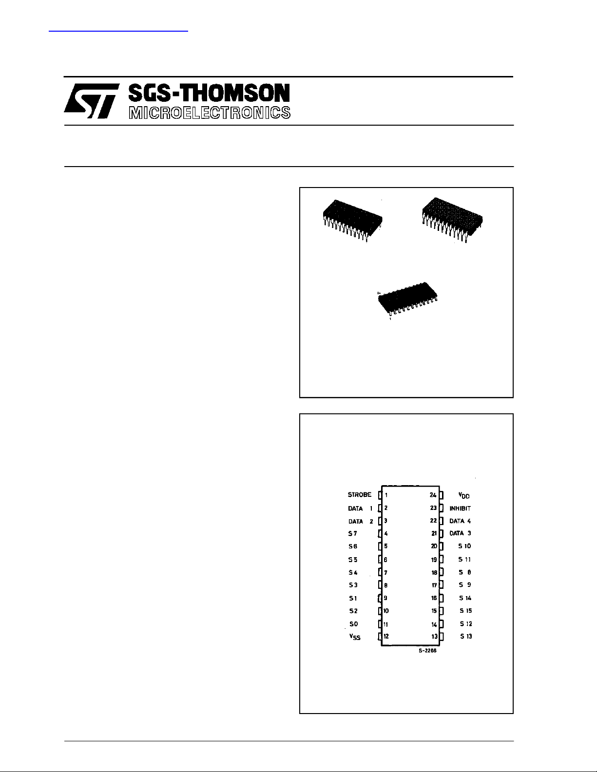
EY
(Plastic Package)
(MicroPackage)
ORDERCODES :
HCC45XXBF HCF45XXBEY
(CeramicFritSeal Package)
M1
F
HCF45XXBM1
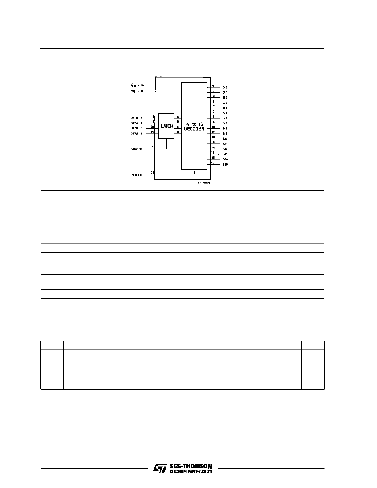
DESCRIPTION
TheHCC4514B/HCC4515B (extended temperature
range)andtheHCF4514B/HCF4515B (intermediate
temperaturerange)are monolithicintegrated circuits
available in 24-lead dual in-line plastic or ceramic
package and plastic micro package. The
HCC/HCF4514B/4515B consistingof a 4-bit strobed
latchand a 4 to 16line decoder. Thelatchesholdthe
last input datapresented prior to the strobe transition
from 1 to 0. Inhibit control allows all outputs to be
placedat0(HCC/HCF4514B)or1(HCC/HCF4515B)
regardless ofthestateofthedataorstrobeinputs.The
decode truth table indicates all combinations ofdata
inputsandappropriate selected outputs.
PIN CONNEC TI O NS
June1989
1/11
HCC/HCF4514B/4515B
FUNCTIONAL DIAGRAM
ABSOLUTE MAXIMUM RATI NG S
Symbol Parameter Val ue Unit
V
* Supply Voltage :HCC Types
DD
HCF Types
V
Input Voltage – 0.5 to VDD+ 0.5 V
i
I
DC Input Current (any one input) ± 10 mA
I
P
Total Power Dissipation (per package)
tot
Dissipation per Output Transistor
for Top= Full Package-temperature Range
T
Operating Temperature : HCC Types
op
HCF Types
T
Stresses above those listed under ”Absolute Maximum Ratings” may cause permanent damage to the device. This is a stress
rating only and functional operation of the device at these or any other conditions above those indicated in the operational sections of this specification is not implied. Exposure to absolute maximum rating conditions for external periods may affect device
reliability.
Storage Temperature – 65 to + 150 °C
stg
– 0.5 to + 20
– 0.5 to + 18
200
100
–55to+125
–40to+85
V
V
mW
mW
°C
°C
RECOMMENDED OPERATING CONDITIONS
Symbol Parameter Value Unit
V
T
2/11
Supply Voltage : HCC Types
DD
HCF Types
V
Input Voltage 0 to V
I
Operating Temperature : HCC Types
op
HCF Types
3to18
3to15
DD
– 55 to + 125
–40to+85
V
V
V
°C
°C
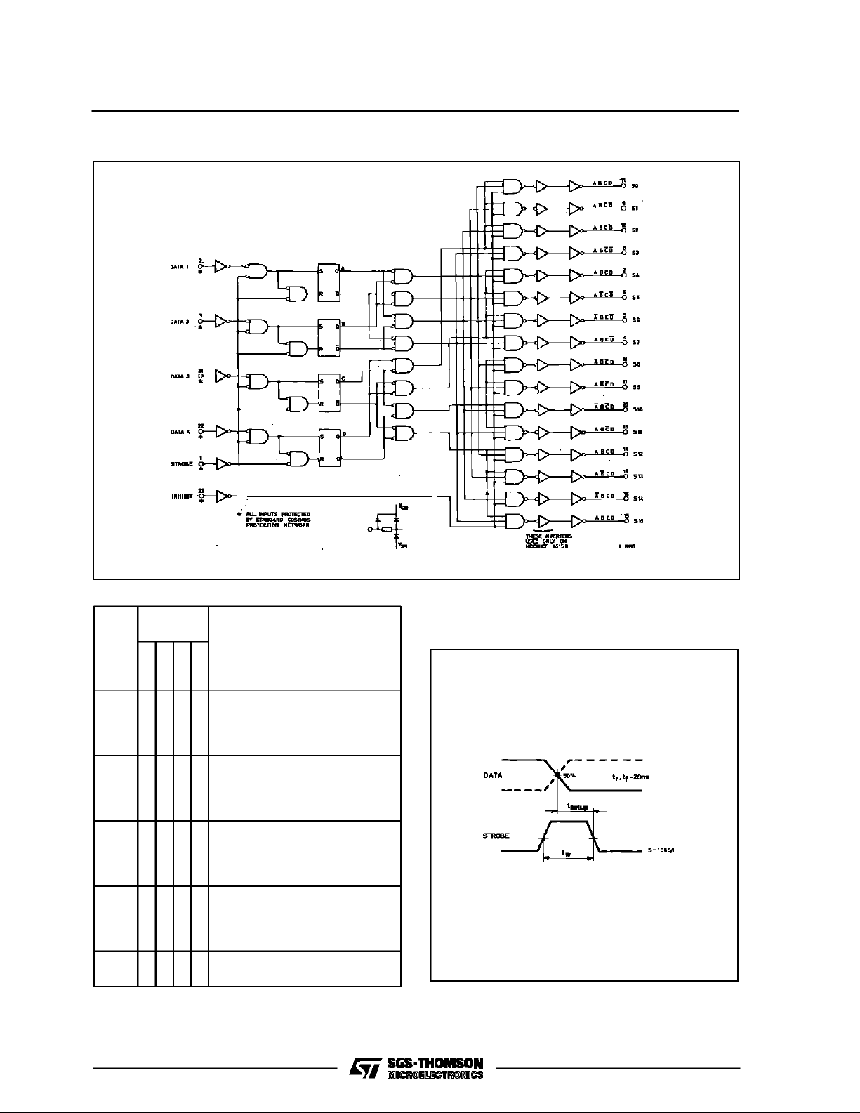
LOGIC DIAGRAM AND TRUTH TABLE
HCC/HCF4514B/4515B
Strobe = 1
Data
Inhibit
X = Don’t Care
1 = high
Inputs
DCBA
0
0
0
0
0
0
0
0
0
0
0
0
1
0
0
1
0
0
1
0
0
1
0
0
0
1
0
0
1
0
0
1
0
0
1
0
1
1
0
1
1
0
1
1
0
1
1
0
1 XXXX
Sel e cted Output
HCC/HCF 4514B = Logic 1
(High)
HCC/HCF 4515B = Logic 0
(Low)
0
0
1
0
0
1
1
1
0
0
1
0
0
1
1
1
0
0
1
0
0
1
1
1
0
0
1
0
0
1
1
1
All Outputs = 0, HCC/HCF 4514B
All Outputs = 1, HCC/HCF 4515B
S0
S1
S2
S3
S4
S5
S6
S7
S8
S9
S10
S11
S12
S13
S14
S15
WAVEFORMS
Setup Timeand Strobe Pulse Width.
3/11
HCC/HCF4514B/4515B
STATIC ELECTRICAL CHARACTERISTICS (over recommended operating conditions)
Test Conditions Valu e
Symbol Parameter
Quiescent
I
L
Current
HCC
Types
HCF
Types
V
OH
Output High
Voltage
V
OL
Output Low
Voltage
V
IH
Input High
Voltage
V
IL
Input Low
Voltage
I
OH
Output
Drive
Current
HCC
Types
HCF
Types
I
OL
Output
Sink
Current
HCC
Types
HCF
Types
I
IH,IIL
Input
Leakage
HCC
Types
Current
HCF
Types
C
Input Capacitance Any Input 5 7.5 pF
I
*T
=–55°CforHCC device : – 40°CforHCF device.
Low
*T
=+125°C for HCC device : + 85°C for HCF device.
High
TheNoise Margin for both”1” and”0” level is : 1V min. with VDD=5V, 2V min. withVDD= 10V,2.5 V min.with VDD= 15V.
V
V
O
|IO|V
I
(V) (V) (µA) (V)
T
DD
* 25°CT
Low
Min. Max. Min. Typ. Max. Min. Max.
High
0/ 5 5 5 0.04 5 150
0/10 10 10 0.04 10 300
0/15 15 20 0.04 20 600
0/20 20 100 0.08 100 3000
0/ 5 5 20 0.04 20 150
0/10 10 40 0.04 40 300
0/15 15 80 0.04 80 600
0/ 5 < 1 5 4.95 4.95 4.95
0/10 < 1 10 9.95 9.95 9.95
0/15 < 1 15 14.95 14.95 14.95
5/0 < 1 5 0.05 0.05 0.05
10/0 < 1 10 0.05 0.05 0.05
15/0 < 1 15 0.05 0.05 0.05
0.5/4.5 < 1 5 3.5 3.5 3.5
1/9 < 1 10 7 7 7
1.5/13.5 < 1 15 11 11 11
4.5/0.5 < 1 5 1.5 1.5 1.5
9/1 < 1 10 3 3 3
13.5/1.5 < 1 15 4 4 4
0/ 5 2.5 5 – 2 – 1.6 – 3.2 – 1.15
0/ 5 4.6 5 – 0.64 – 0.51 – 1 – 0.36
0/10 9.5 10 – 1.6 – 1.3 – 2.6 – 0.9
0/15 13.5 15 – 4.2 – 3.4 – 6.8 – 2.4
0/ 5 2.5 5 – 1.53 – 1.36 – 3.2 – 1.1
0/ 5 4.6 5 – 0.52 – 0.44 – 1 – 0.36
0/10 9.5 10 – 1.3 – 1.1 – 2.6 – 0.9
0/15 13.5 15 – 3.6 – 3.0 – 6.8 – 2.4
0/ 5 0.4 5 0.64 0.51 1 0.36
0/10 0.5 10 1.6 1.3 2.6 0.9
0/15 1.5 15 4.2 3.4 6.8 2.4
0/ 5 0.4 5 0.52 0.44 1 0.36
0/10 0.5 10 1.3 1.1 2.6 0.9
0/15 1.5 15 3.6 3.0 6.8 2.4
0/18
18 ± 0.1 ±10
–5
± 0.1 ± 1
Any Input
0/15
15 ± 0.3 ±10
–5
± 0.3 ± 1
Unit
*
µA
V
V
V
V
mA
mA
µA
4/11

DYNAMIC ELECTRICAL CHARACTERISTICS
(T
=25°C, CL= 50pF, RL= 200kΩ, allinput rise andfall time = 20ns)
amb
Symbol Parameter
t
,
PHL
t
PLH
t
THL
t
THL
t
t
se tu p
Propagation Delay Time
,
Transition Time 5 100 200
Strobe Pulse Width 5 250 125
W
Setup Time 5 150 75
Test Conditions Value
Strobe or Data
Inhibit
HCC/HCF4514B/4515B
V
(V) Min. Typ. Max.
DD
5485970
10 185 370
15 135 270
5250500
10 110 220
15 85 170
10 50 100
15 40 80
10 100 50
15 75 40
10 70 35
15 40 20
Unit
ns
ns
ns
ns
ns
TypicalOutput Low (sink)Current Characteristics. MinimumOutputLow(sink)CurrentCharacteristics.
5/11

HCC/HCF4514B/4515B
Typical Output High (source) Current Characteristics.
Typical Strobe or Data Propagation Delay Timevs.
Load Capacitance.
Minimum Output High (source) Current Characteristics.
TypicalInhibit Propagation DelayTimevs.LoadCapacitance.
TypicalTransitionTime vs. Load Capacitance.
6/11
TypicalStrobe orData Propagation Delay Time vs.
Supply Voltage.

Typical Power Dissipationvs. Frequency.
TEST CIRCUITS
HCC/HCF4514B/4515B
Quiescent Device Current.
Input Leakage Current.
Noise Immunity.
7/11

HCC/HCF4514B/4515B
Plastic DIP24 (0.25) MECHANICAL DATA
DIM.
MIN. TYP. MAX. MIN. TYP. MAX.
a1 0.63 0.025
b 0.45 0.018
b1 0.23 0.31 0.009 0.012
b2 1.27 0.050
D 32.2 1.268
E 15.2 16.68 0.598 0.657
e 2.54 0.100
e3 27.94 1.100
F 14.1 0.555
I 4.445 0.175
L 3.3 0.130
mm inch
8/11
P043A

Ceramic DIP24 MECHANICAL DATA
HCC/HCF4514B/4515B
DIM.
MIN. TYP. MAX. MIN. TYP. MAX.
A 32.3 1.272
B 13.05 13.36 0.514 0.526
C 3.9 5.08 0.154 0.200
D 3 0.118
E 0.5 1.78 0.020 0.070
e3 27.94 1.100
F 2.29 2.79 0.090 0.110
G 0.4 0.55 0.016 0.022
I 1.17 1.52 0.046 0.060
L 0.22 0.31 0.009 0.012
M 1.52 2.49 0.060 0.098
N1
P 15.4 15.8 0.606 0.622
Q 5.71 0.225
4° (min.), 15° (max.)
mm inch
P058C
9/11

HCC/HCF4514B/4515B
SO24 MECHANICAL DATA
DIM.
MIN. TYP. MAX. MIN. TYP. MAX.
A 2.65 0.104
a1 0.10 0.20 0.004 0.007
a2 2.45 0.096
b 0.35 0.49 0.013 0.019
b1 0.23 0.32 0.009 0.012
C 0.50 0.020
c1 45° (typ.)
D 15.20 15.60 0.598 0.614
E 10.00 10.65 0.393 0.420
e 1.27 0.05
e3 13.97 0.55
F 7.40 7.60 0.291 0.299
L 0.50 1.27 0.19 0.050
S8°(max.)
mm inch
L
A
a2
b
e3
D
24 13
112
e
F
s
a1
c1
b1
C
E
10/11

HCC/HCF4514B/4515B
Information furnished is believed to be accurate and reliable. However, SGS-THOMSON Microelectronics assumes no responsability for the
consequences of use of such information nor for any infringement of patents or other rights of third parties which may results from its use. No
license is granted by implication or otherwise underany patent or patent rights of SGS-THOMSON Microelectronics. Specificationsmentioned
in this publication are subject to change without notice. This publication supersedes and replaces all information previously supplied.
SGS-THOMSON Microelectronicsproductsare notauthorized for use ascritical componentsinlife supportdevices or systemswithout express
written approval of SGS-THOMSON Microelectonics.
1994 SGS-THOMSON Microelectronics - All Rights Reserved
Australia - Brazil - France - Germany - Hong Kong - Italy - Japan - Korea - Malaysia - Malta - Morocco - The Netherlands -
Singapore - Spain - Sweden - Switzerland - Taiwan - Thailand - UnitedKingdom - U.S.A
SGS-THOMSON Microelectronics GROUP OF COMPANIES
11/11
 Loading...