

查询HCC4073B供应商
4073B TRIPLE 3–INPU T AND G AT E
4081B QUAD 2–INPUT AND GATE
4082B DUAL 4–INPUT AND GATE
HCC4073B/81B/82B
HCF4073B/81B/82B
AND GATES
. MEDIUM SPEED OPERATION – t
(typ.); t
= 65ns (typ.)AT 10V
PHL
PLH
= 85ns
.QUIESCENT CURRENT SPECIFIED TO 20V
FOR HCC DEVICE
.5V, 10V, AND 15V PARAMETRIC RATINGS
.INPUT CURRENT OF 100nA AT 18V AND
25°C FORHCC DEVICE
.100% TESTEDFOR QUIESCENTCURRENT
.MEETSALLREQUIREMENTSOFJEDECTEN-
TATIVESTANDARDN°13A,”STANDARDSPECIFICATIONS FOR DESCRIPTION OF ”B”
SERIESCMOS DEVICES”
DESCRIPT ION
The HCC4073B, HCC4081B and HCC4082B (ex-
tended temperature range) and the HCF4073B,
HCF4081B and HCF4082B (intermediate temperature range) are monolithic integrated circuitsavail-
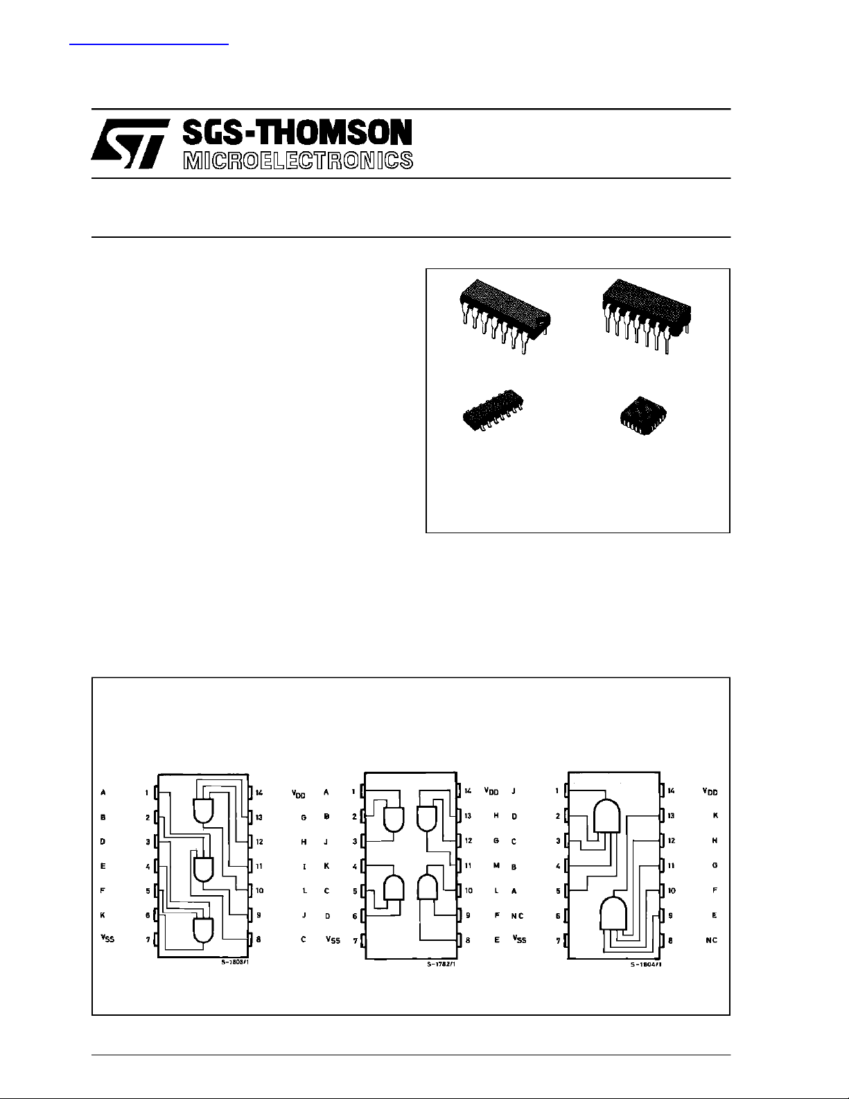
CONN E CTION DIAG RAM
4073B 4081B 4082B
EY
(Plastic Package)F(Ceramic FritSealPackage)
M1
(MicroPackage)
ORDER CODES :
HCC40XXBF HCF40XXBM1
HCF40XXBEY HCF40XXBC1
able in 14-leaddual in-line plastic or ceramicpackage and plasticmicro package.
The HCC/HCF4073B, 4081B and 4082B AND
gates provide the system designer with direct im-
(Plastic Chip Carrier)
C1
June1989
1/10
HCC/H CF4073B/4081B/4082B
ABSOLUTE MAXIMUM RATI N GS
Symbol Parameter Value Unit
V
* Supply Voltage :HCC Types
DD
HCF Types
V
Input Voltage – 0.5 to VDD+ 0.5 V
i
I
DC Input Current (any one input) ± 10 mA
I
P
Total Power Dissipation (per package)
tot
Dissipation per Output Transistor
for T
T
Operating Temperature : HCC Types
op
= Full Package-temperature Range
op
HCF Types
T
Stresses above those listed under ”Absolute Maximum Ratings” may cause permanent damage to the device. This is a stress
rating only and functional operation of the device at these or any other conditions above those indicated in the operational sections of this specification is not implied. Exposure to absolute maximum rating conditions for external periods may affect device
reliability.
* All voltage values are referred to VSSpin voltage.
Storage Temperature – 65 to + 150 °C
stg
RECOMMENDED OPERATING C ONDITIONS
Symbol Parameter Value Unit
V
T
Supply Voltage : HCC Types
DD
HCF Types
V
Input Voltage 0 to V
I
Operating Temperature : HCC Types
op
HCF Types
– 0.5 to + 20
– 0.5 to + 18
200
100
– 55 to + 125
–40to+85
3to18
3to15
DD
– 55 to + 125
–40to+85
V
V
mW
mW
°C
°C
V
V
V
°C
°C
STATIC ELECTRICAL CHARACTERISTICS (over recommended operating conditions)
Test Conditions Valu e
Symbol Parameter
I
Quiescent
L
Current
HCC
Types
HCF
Types
V
OH
Output High
Voltage
V
OL
Output Low
Voltage
*T
*T
=–55°C for HCC device : – 40°C for HCF device.
Low
=+125°C for HCC device : + 85°C for HCF device.
High
The Noise Margin for both ”1” and ”0” level is : 1V min. with VDD= 5V, 2V min. with VDD= 10V, 2.5V min. with VDD= 15V.
V
V
O
|IO|V
I
(V) (V) (µA) (V)
T
DD
*25°CT
Low
Min. Max. Min. Typ. Ma x. Min. Max.
High
*
0/ 5 5 0.25 0.01 0.25 7.5
0/10 10 0.5 0.01 0.5 15
0/15 15 1 0.01 1 30
0/20 20 5 0.02 5 150
0/ 5 5 1 0.01 1 7.5
0/10 10 2 0.01 2 15
0/15 15 4 0.01 4 30
0/ 5 < 1 5 4.95 4.95 4.95
0/10 < 1 10 9.95 9.95 9.95
0/15 < 1 15 14.95 14.95 14.95
5/0 < 1 5 0.05 0.05 0.05
10/0 < 1 10 0.05 0.05 0.05
15/0 < 1 15 0.05 0.05 0.05
Unit
µA
V
V
2/10
HCC/HCF4073B/4081B/4082B
STATIC ELECTRICAL CHARACTERISTICS (continued)
Test Conditions Valu e
Symbol Parameter
(V) (V) (µA) (V)
V
IH
Input High
Voltage
V
IL
Input Low
Voltage
I
OH
Output
Drive
Current
HCC
Types
0/ 5 2.5 5 – 2 – 1.6 – 3.2 – 1.15
0/ 5 4.6 5 – 0.64 – 0.51 – 1 – 0.36
0/10 9.5 10 – 1.6 – 1.3 – 2.6 – 0.9
0/15 13.5 15 – 4.2 – 3.4 – 6.8 – 2.4
0/ 5 2.5 5 – 1.53 – 1.36 – 3.2 – 1.1
HCF
Types
0/ 5 4.6 5 – 0.52 – 0.44 – 1 – 0.36
0/10 9.5 10 – 1.3 – 1.1 – 2.6 – 0.9
0/15 13.5 15 – 3.6 – 3.0 – 6.8 – 2.4
I
OL
Output
Sink
Current
HCC
Types
0/ 5 0.4 5 0.64 0.51 1 0.36
0/10 0.5 10 1.6 1.3 2.6 0.9
0/15 1.5 15 4.2 3.4 6.8 2.4
0/ 5 0.4 5 0.52 0.44 1 0.36
HCF
Types
0/10 0.5 10 1.3 1.1 2.6 0.9
0/15 1.5 15 3.6 3.0 6.8 2.4
I
IH,IIL
*T
*T
Input
Leakage
Current
Input Capacitance Any Input 5 7.5 pF
C
I
=–55°C for HCC device : – 40°C for HCF device.
Low
=+125°C for HCC device : + 85°C for HCF device.
High
The Noise Margin for both ”1” and ”0” level is : 1V min. with VDD= 5V, 2V min. with VDD= 10V, 2.5V min. with VDD= 15V.
HCC
Types
HCF
Types
0/18
0/15
V
V
I
O
|IO|V
DD
T
*25°CT
Low
Min. Max. Min. Typ. Ma x. Min. Max.
0.5/4.5 < 1 5 3.5 3.5 3.5
1/9 < 1 10 7 7 7
1.5/13.5 < 1 15 11 11 11
4.5/0.5 < 1 5 1.5 1.5 1.5
9/1 < 1 10 3 3 3
13.5/1.5 < 1 15 4 4 4
18 ± 0.1 ±10
–5
± 0.1 ± 1
Any Input
–5
15 ± 0.3 ±10
± 0.3 ± 1
High
*
Unit
V
V
mA
mA
µA
DYNAMIC ELECTRICAL CHARACTERISTICS (T
=25°C, CL= 50pF, typical temperature
amb
coefficient for all VDDvalues is 0.3%/°C, all input rise and fall times = 20ns, RL= 200kΩ)
Symbol Paramet e r
t
PHL,tPLH
t
TLH,tTHL
Propagation Delay Time 5 125 250
Transition Time 5 100 200
Test Conditions
(V) Min. Typ. Max.
V
DD
10 60 125
15 45 90
10 50 100
15 40 80
Value
Unit
ns
ns
3/10

HCC/H CF4073B/4081B/4082B
TypicalVoltage and Current Transfer Characteristics.
Minimum Output Low (sink) Current Characteristics.
Typical OutputLow (sink) Current .
Typical Output High (source) Current Characteristics.
Minimum Output High (source) Current Characteristics.
4/10
Typical Propagation Delay Time vs. Load Capacitance.

HCC/HCF4073B/4081B/4082B
TypicalTransitionTime vs. Load Capacitance.
TEST CIRCUITS
Typical Dynamic Power Dissipation per Gate vs.
Frequency.
Input Voltage.QuiescentDevice Current.
Input Leakage Current.
5/10

HCC/H CF4073B/4081B/4082B
Plastic DIP14 MECHANICAL DATA
DIM.
MIN. TYP. MAX. MIN. TYP. MAX.
a1 0.51 0.020
B 1.39 1.65 0.055 0.065
b 0.5 0.020
b1 0.25 0.010
D 20 0.787
E 8.5 0.335
e 2.54 0.100
e3 15.24 0.600
F 7.1 0.280
I 5.1 0.201
L 3.3 0.130
Z 1.27 2.54 0.050 0.100
mm inch
6/10
P001A

HCC/HCF4073B/4081B/4082B
Ceramic DIP14/1 MECHANICAL DATA
DIM.
MIN. TYP. MAX. MIN. TYP. MAX.
A 20 0.787
B 7.0 0.276
D 3.3 0.130
E 0.38 0.015
e3 15.24 0.600
F 2.29 2.79 0.090 0.110
G 0.4 0.55 0.016 0.022
H 1.17 1.52 0.046 0.060
L 0.22 0.31 0.009 0.012
M 1.52 2.54 0.060 0.100
N 10.3 0.406
P 7.8 8.05 0.307 0.317
Q 5.08 0.200
mm inch
P053C
7/10

HCC/H CF4073B/4081B/4082B
SO14 MECHANICAL DATA
DIM.
MIN. TYP. MAX. MIN. TYP. MAX.
A 1.75 0.068
a1 0.1 0.2 0.003 0.007
a2 1.65 0.064
b 0.35 0.46 0.013 0.018
b1 0.19 0.25 0.007 0.010
C 0.5 0.019
c1 45° (typ.)
D 8.55 8.75 0.336 0.344
E 5.8 6.2 0.228 0.244
e 1.27 0.050
e3 7.62 0.300
F 3.8 4.0 0.149 0.157
G 4.6 5.3 0.181 0.208
L 0.5 1.27 0.019 0.050
M 0.68 0.026
S8°(max.)
mm inch
8/10
P013G

HCC/HCF4073B/4081B/4082B
PLCC20 MECHANICAL DATA
DIM.
MIN. TYP. MAX. MIN. TYP. MAX.
A 9.78 10.03 0.385 0.395
B 8.89 9.04 0.350 0.356
D 4.2 4.57 0.165 0.180
d1 2.54 0.100
d2 0.56 0.022
E 7.37 8.38 0.290 0.330
e 1.27 0.050
e3 5.08 0.200
F 0.38 0.015
G 0.101 0.004
M 1.27 0.050
M1 1.14 0.045
mm inch
P027A
9/10

HCC/H CF4073B/4081B/4082B
Information furnished is believed tobe accurate and reliable. However, SGS-THOMSON Microelectronics assumes no responsability for the
consequences of use of such information nor for any infringement of patents or other rights of third parties which may results from its use. No
license is grantedby implication or otherwise underany patentor patent rights of SGS-THOMSON Microelectronics. Specificationsmentioned
in this publicationare subject to changewithout notice. This publication supersedes andreplaces all information previously supplied.
SGS-THOMSON Microelectronicsproductsare notauthorized foruse ascritical componentsin life supportdevices or systemswithout express
written approval of SGS-THOMSON Microelectonics.
1994 SGS-THOMSON Microelectronics- All RightsReserved
Australia - Brazil - France - Germany - Hong Kong - Italy - Japan - Korea - Malaysia - Malta - Morocco - The Netherlands -
Singapore - Spain - Sweden - Switzerland - Taiwan - Thailand - United Kingdom - U.S.A
SGS-THOMSON Microelectronics GROUP OF COMPANIES
10/10
 Loading...