

查询BTA06 SW供应商
FEATURES
BTA0 6 TW/S W
BTB0 6 TW/S W
LOGIC LEVEL TRIACS
.LOWI
.LOW I
= 5mA max
GT
= 15mA max
H
.HIGH EFFICIENCYSWITCHING
.BTA Family:
INSULATINGVOLTAGE= 2500V
(ULRECOGNIZED: E81734)
DESCRIPTION
The BTA/BTB06 TW/SW use high performance
products glass passivated chips.
The low I
ciency circuit make this family will adapted for low
power trigger circuits (microcontrollers, microprocessors, integrated circuits ...)
ABSOLUTE RATINGS (limiting values)
Symbol Parameter Value Unit
I
T(RMS)
GT/IH
I
TSM
I2tI
level coupled with the high effi-
RMS on-state current
(360° conduction angle)
Non repetitive surge peak on-state current
( Tj initial = 25°C)
2
t value tp = 10 ms 18 A2s
(RMS)
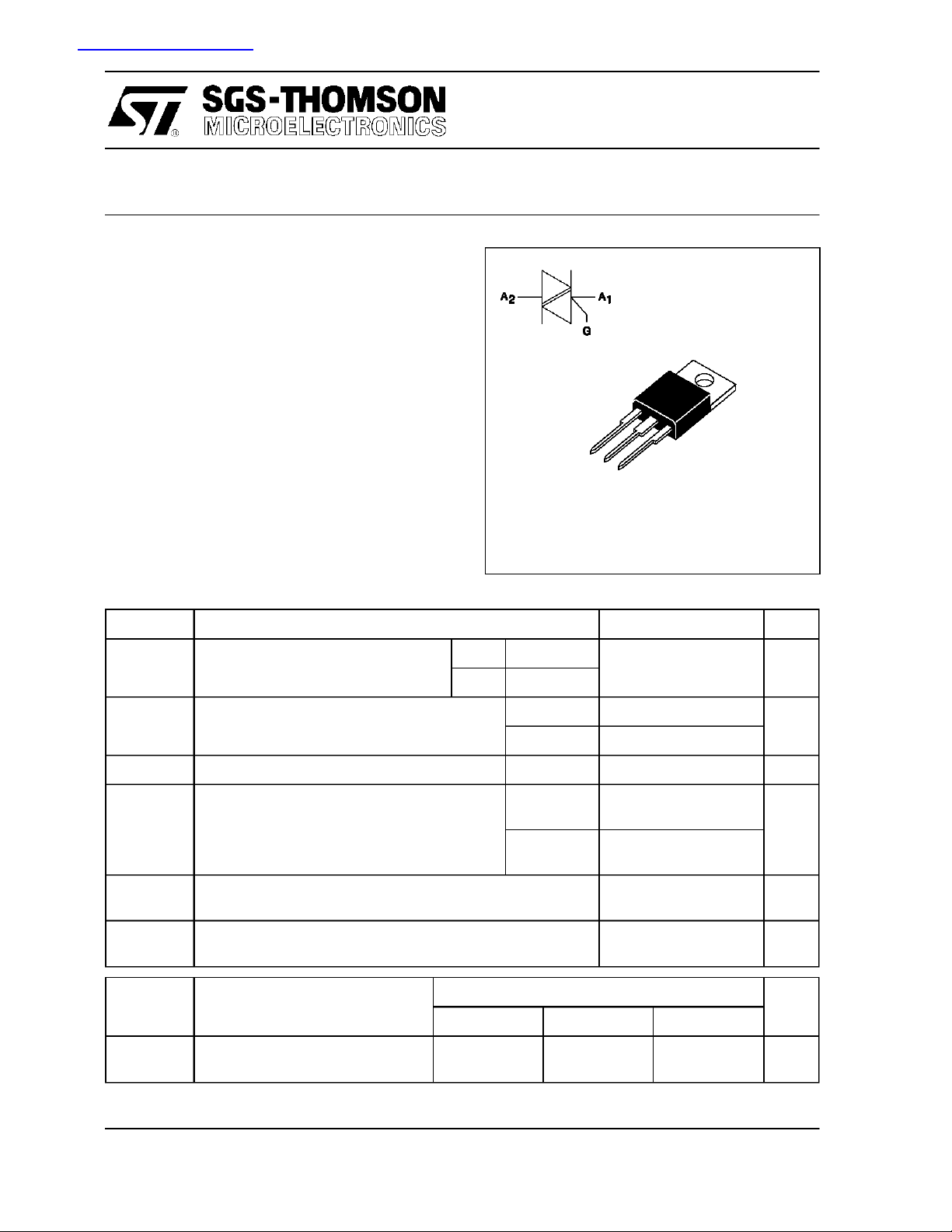
A1
A2
G
TO220AB
(Plastic)
BTA Tc = 80 °C6 A
BTB Tc = 90 °C
tp = 8.3 ms 63 A
tp = 10 ms 60
dI/dt Critical rate of rise of on-state current
Gate supply : IG= 50mA diG/dt = 0.1A/µs
Tstg
Tj
Tl Maximum lead temperature for soldering during 10 s at 4.5 mm
Symbol Parameter BTA / BTB06- Unit
V
DRM
V
RRM
March 1995
Storage and operating junction temperature range - 40 to + 150
from case
400 TW/SW 600 TW/SW 700 TW/SW
Repetitive peak off-state voltage
Tj = 110 °C
Repetitive
F = 50 Hz
Non
Repetitive
400 600 700 V
20 A/µs
100
- 40 to + 110
260 °C
°C
°C
1/5
BTA 0 6 TW/SW / BTB06 TW/ SW
THERMAL RESISTANCES
Symbol Parameter Value Unit
Rth (j-a) Junction to ambient 60 °C/W
Rth (j-c) DC Junction to case for DC BTA 4.4 °C/W
BTB 3.3
Rth (j-c) AC Junction to case for 360° conduction angle
( F= 50 Hz)
BTA 3.3 °C/W
BTB 2.5
GATECHARACTERISTICS (maximum values)
P
G (AV)
=1W PGM= 10W (tp = 20 µs) IGM=4A(tp=20µs) VGM= 16V (tp = 20 µs).
ELECTRICAL CHARACTERISTICS
Symbol Test Conditions Quadrant Suffix Unit
TW SW
I
GT
V
GT
V
GD
tgt VD=V
I
L
IH*I
VTM*ITM= 8.5A tp= 380µs Tj=25°C MAX 1.75 V
VD=12V (DC) RL=33Ω Tj=25°C I-II-III MAX 5 10 mA
VD=12V (DC) RL=33Ω Tj=25°C I-II-III MAX 1.5 V
VD=V
DRMRL
DRMIG
dIG/dt = 0.5A/µs
IG=1.2 I
= 100mA gate open Tj=25°C MAX 15 25 mA
T
=3.3kΩ Tj=110°C I-II-III MIN 0.2 V
= 40mA
GT
Tj=25°C I-II-III TYP 2 µs
Tj=25°C I-III TYP 8 15 mA
II 15 25
I
DRM
I
RRM
dV/dt * Linear slope up to VD=67%V
(dI/dt)c * dV/dt= 0.1V/µs Tj=110°C MIN 2.7 3.5 A/ms
* For either polarity of electrode A2voltage with referenceto electrode A1.
2/5
V
V
gate open
dV/dt= 20V/µs MIN 1.3 2.7
DRM
RRM
Rated
Rated
DRM
Tj=25°C MAX 0.01 mA
Tj=110°C MAX 1
Tj=110°C MIN 20 50 V/µs
 Loading...