

Page 1

AV321T
servicemanual
Page 2

Catalog
ChapterOneAboutMaintenance
1.1Safetyprecautions
1.1.1Powersupply
1.1.2Precautionsforantistatic
1.1.3Aboutplacementposition
1.2Maintenancemethod
1.2.1Visualizedmethod
1.2.2Electricresistancemethod
1.2.3Voltagemethod
1.2.4Currentmethod
1.2.5Cuttingmethod
1.2.6Elementsubstitutionmethod
1.2.7Comparisonmethod
1.3Requireddeviceformaintenance
1
1
1
1
2
2
2
2
2
2
2
3
3
3
ChapterTwoFunctionsandOperationInstructions
2.1FEATURES
2.2ControlbuttonlocationsandExplanations
2.2.1Frontpanelfunctionsandillustrations
2.2.2VFDDISPLAY
2.2.3REARPANELILLUSTRATIONS
2.2.4REARPANELILLUSTRATIONS
2.3BASICOPERATIONS
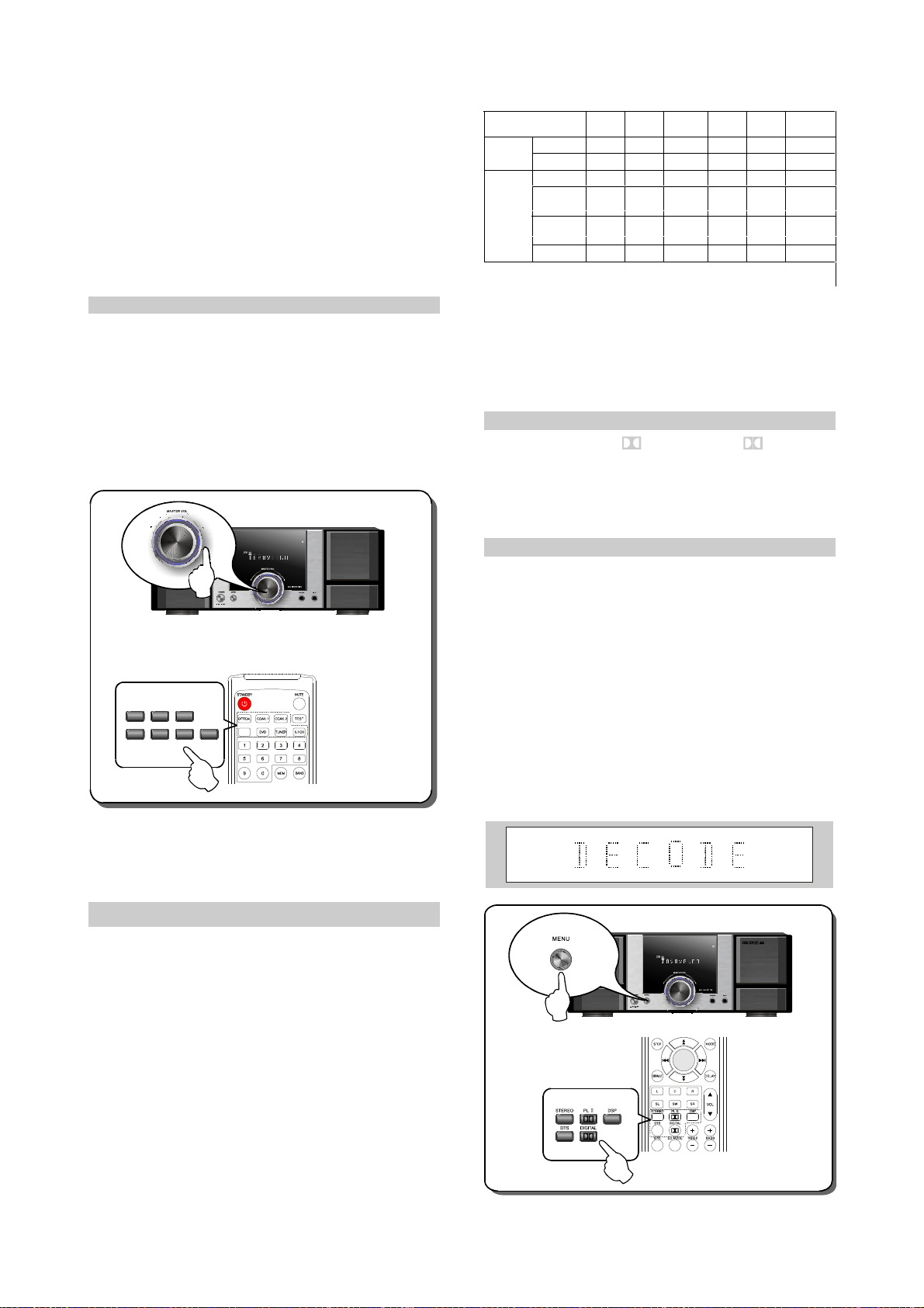
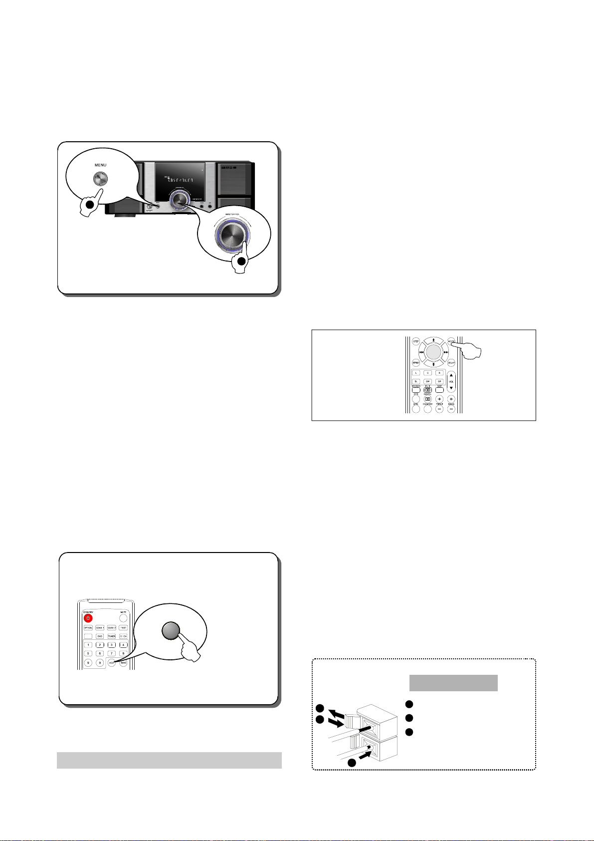
2.3.1TurnOn/OfftheUnit
2.3.2Mute
2.3.3SelectInputSoundSourceandVideoSource
2.3.4SelectDecodeMode
2.3.5AdjustVolume
2.3.6AdjustChannelLevel
2.3.7AdjustMainChannelTone
4
4
4
4
5
5
6
7
7
7
7
8
8
9
9
Page 3

2.3.8SelectEQMode
9
2.3.9DEFAULT
2.3.10Karaoke
2.3.11Tuning
2.3.12Tuning(Continued)
2.3.13ChannelDelay
2.3.14NoiseTesting
2.3.15SelectSpeakerMode
2.3.16Headphone
2.4ACCESSORIES
2.5SPECIFICATIONS
ChapterThreeUnitCircuitPrinciple
SectionOnePrincipleoftheplayer
3.1.1Compositionoftheplayer
3.1.2Functionandfeatures
9
9
10
11
12
12
12
12
13
13
14
14
14
14
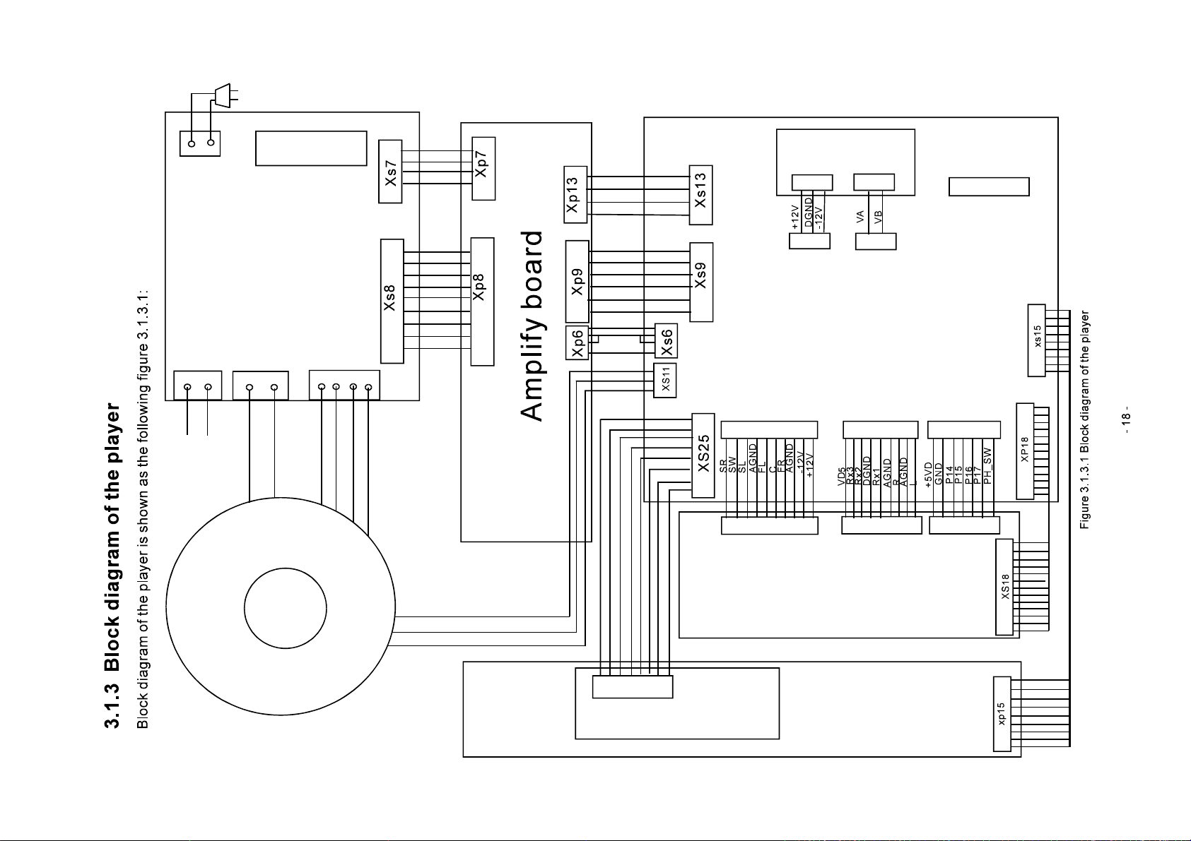
3.1.3Blockdiagramoftheplayer
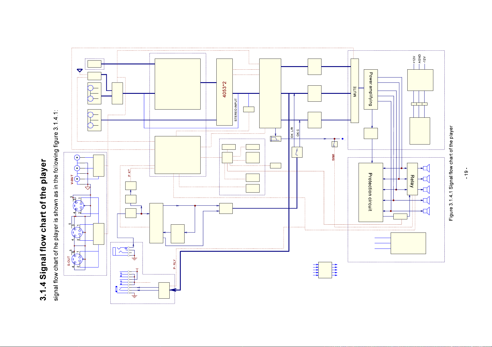
3.1.4Signalflowchartoftheplayer
SectionTwoUnitCircuitPrinciple
3.2.1Signalprocessingboard
3.2.2Decodeboard
3.2.3Controlpanel
3.2.4Powerboard
3.2.5Poweramplifierboardandprotectioncircuit
3.2.6Videoinput/outputboard
3.2.7MIC,headphoneboard
SectionThreeServicingCases
3.3.1Servicingcases
3.3.2Troubleshootingflowchart
SectionFourServicingParameter
3.4.1Signalwaveformdiagram
15
16
17
17
18
19
20
21
24
24
26
26
32
37
37
3.4.2Keypointvoltage
SectionFiveFunctionIntroductiontoIC
3.5.1functionintroductionto4558
3.5.2functionintroductiontoPt2399
47
48
48
49
Page 4

3.5.3functionintroductiontoCd4051
50
3.5.4functionintroductiontoCd4052
3.5.5functionintroductiontoCd4053
3.5.6functionintroductiontoPt6311
3.5.7functionintroductiontoUTCLM4880
3.5.8functionintroductionto74HC04
3.5.9functionintroductiontoLm1875
3.5.10functionintroductiontoTDA2052
3.5.11functionintroductiontoM62446
3.5.12functionintroductiontoAT24C02
3.5.13functionintroductiontoL7805
3.5.14functionintroductionto7812
3.5.15functionintroductionto7912
3.5.16functionintroductiontoNe5532
3.5.17functionintroductiontoPt2315
3.5.18functionintroductiontoCs4360
51
52
53
56
56
57
58
59
61
62
62
63
63
64
66
3.5.19functionintroductiontoCd4094
3.5.20functionintroductiontoCs5340
3.5.21functionintroductiontoCs8415
3.5.22functionintroductiontoCs49326
ChapterFourDisassemblyandAssemblyProcess
ChapterCinquePCBboard&Circuitdiagram
SectionOnePCB
BoardSectionTwocircuitdiagram
ChaptersixBOMList
6.1SIGNALDISPOSALBOARD
6.2SIGNALDISPOSALBOARDAISEGMENT
6.3DECODEBOARD
67
68
70
71
74
75
75
83
93
93
93
96
6.4DECODEBOARD-SMD
6.5AMPLIFIERBOARD
6.6SURFACECONTROLBOARD
6.7POWERBOARD
96
98
101
102
Page 5

6.8MICROPHONEHOLDERBOARD
104
6.9VIDEOFREQUENCYBOARD
6.10REMOTECONEROLLER
6.11PANELUNIT
6.12PROGRAMCPU
6.13SNLABEL
6.14SUPPLEMENTMODULE
104
105
106
106
106
107
Page 6

ChapterOneAboutMaintenance
1.1Safetyprecautions
1.1.1Powersupply
Whenservicingaudiopoweramplifier,theservicingpersonnelpayspecialattentiontothepower
boardwith220VAC,orelsetheimproperoperationwillleadtobodydamage.Thealternatecurrent
whichoutputstopoweramplifierboardthroughpowerboardisalsouptovoltagewithabout50V;when
servicing,short-circuitandjointweldingcannotoccur,orelsetheelementswillbeburntoutandtrouble
rangewillbeenlarged.
1.1.2Precautionsforantistatic
Movementandfrictionwillbothbringstaticelectricitywhichcausesseriousdamagestointegrated
IC.Thoughstaticchargeislittle,whenalimitedquantityofelectricchargeisaddedtolargescaleintegratedIC,asthecapacitanceisverysmallinthemeantime,nowtheintegratedICisverymuch
easytobestruckthroughbystaticelectricityortheperformancewilldecrease.Thusstaticelectricity
preventionisofextraordinaryimportance.Thefollowingareseveralmeasurestopreventstatic
electricity:
1.Useapieceofelectricconductionmetalwiththelengthofabout2metrestoinsertintotheearth,
andFetchtheleadwirefromthetopofthesurplusmetalandconnecttotherequiredstaticelectricity
device.Thelengthanddepthofthemetalembeddedundertheearthshouldbedeterminedaccordingto
thewettabilityofthelocalsoil.Forhumidplaces,itmaybeshorter,andlongeranddeeperfordryplaces.
Ifpossible,itcanbedistributedandlayedintermsof“#”shape.
2.Onoperatingtable-board,theantistatictablecushionshouldbecoveredandgrounded.
3.Alldevicesandequipmentsshouldbeplacedontheantistatictablecushionandgrounded.
4.Maintenancepersonnelshouldwearantistaticwristringwhichshouldbegrounded.
5.Placesaroundtheoperatingpositionshouldalsobecoveredwithelectricconductioncushionor
Paintedwithantistaticpaint.
-1-
Page 7

1.1.3Aboutplacementposition
1.
Audiopoweramplifiercannotbeinstalledinplaceswithhightemperatureandhumidity.
2.Positionsforplacementshouldbestableandsecure.
1.2Maintenancemethod
1.2.1Visualizedmethod
Directlyviewwhetherabnormalitiesofcollision,lackofelement,jointwelding,sheddingwelding,
rosinjoint,copperfoilturningup,leadwiredisconnectionandelementsburningupamongpinsof
elementsappear.Checkpowersupplyofthemachineandthenusehandstotouchthecasingofpartof
elementsandcheckwhethertheyarehottojudgethetroublespot.Youshouldpaymoreattentionwhen
usingthismethodtocheckinhighvoltageparts.
1.2.2Electricresistancemethod
Setthemultimeterinresistancepositionandtestwhetherthenumericalvalueofresistanceofeach
pointinthecircuithasdifferencefromthenormalvaluetojudgethetroublespot.Butinthecircuitthe
testednumericalvalueofresistanceisnotaccurate,andthetestednumericalvalueofintegratedIC's
pinscanonlybeusedforreference,sotheelementsshouldbebrokendownfortest.
1.2.3Voltagemethod
Voltagemethodisrelativelyconvenient,quickandaccurate.Setthemultimeterinvoltageposition
andtestpowersupplyvoltageoftheplayerandvoltageofacertainpointtojudgethetroublespot
accordingtothetestedvoltagevariation.
1.2.4Currentmethod
Setthemultimeterincurrentpositionandtestcurrentoftheplayerofacertainpointtojudgethe
troublespot.Butwhentestingincurrentmethod,themultimetershouldbeseriesconnectedinthe
circuit,whichmakesthismethodtootrivialandtroublesome,soitislessfrequentlyusedinreality.
1.2.5Cuttingmethod
Cuttingmethodshouldbecombinedwithelectricresistancemethodandvoltagemethodtouse.
Thismethodismainlyusedinphenomenaofshortcircuitandcurrentleakageofthecircuit.When
cuttingtheinputterminalvoltageofacertainlevel,ifvoltageoftheplayerrisesagain,itmeansthatthe
troubleliesinthislevel.
-2-
Page 8

1.2.6Elementsubstitutionmethod
Whensomeelementscannotbejudgedgoodorbad,substitutionmethodmaydeadopteddirectly.
1.2.7Comparisonmethod
AsamegoodPCboardisusuallyusedtotestthecorrectvoltageandwaveform.Comparedthese
datawiththosetestedthroughfaultPCboard,thecauseoftroublesmaybefound.
Throughtheabovemaintenancemethod,theoreticalknowledgeandmaintenanceexperience,all
difficultiesandtroubleswillbereadilysolved.
1.3Requireddeviceformaintenance
AudioGenerator
◆
Digitaloscillograph(100MHE)
◆≥
SMDreworkstation
◆
Multimeter
◆
Solderingiron
◆
Pointed-monthpincers
◆
Cuttingnippers
◆
Forceps
◆
Electricscrewdriver
◆
Terminalsconnectingcord
◆
Headphone
◆
Microphone
◆
-3-
Page 9

ChapterTwo
FunctionsandOperationInstructions
2.1FEATURES
◆
2-waycoaxialdigitalsignalinput,1-wayopticaldigitalsignalinput
◆
With5.1CHinputterminal,capableofconnectingwithexternalmulti-channeladvanceddecode
outputsignalssuchasDOLBYDIGITAL,DTS
◆
Withsubwooferoutputterminal,capableofconnectingwithactivesubwooferspeaker
◆
Built-inFM/AMtuner
◆
Withheadphoneoutputjack
◆
6CHdigitalvolumecontrol
◆
Separateleveladjustmenttoleft,right,centre,surroundandsubwooferchannel
◆
DolbyDigital,DTS,DolbyProLogicII,DSP,STEREOdecode
◆
Automaticallyrecognizeinputsignalformatandselectthecorrespondingdecodemode
◆
Decodemodemanualselection
◆
Mainchannelhigh/lowtoneadjustment
◆
VideoandS-Videoselectedfunction
◆
Centre,surrounddelayadjustmen
◆
Noisetesting
◆
5presetEQmodes
◆
Digitaltuningfunction
◆
Capableofstoring36FMand12AMradiostations
◆
Automatically/Manuallysearchingradiostations
◆
Automuteifthereisnosignal
◆
High-performancedigitalKaraoke,withMICvolume,toneandechoadjustment
◆
Separate5CHpoweramplification
◆
Speciallyautomaticprotectionofshort-circuit,over-voltageandover-current
◆
Fullremotecontroloperation
t
◆
Completeunitinterface
-4-
Page 10
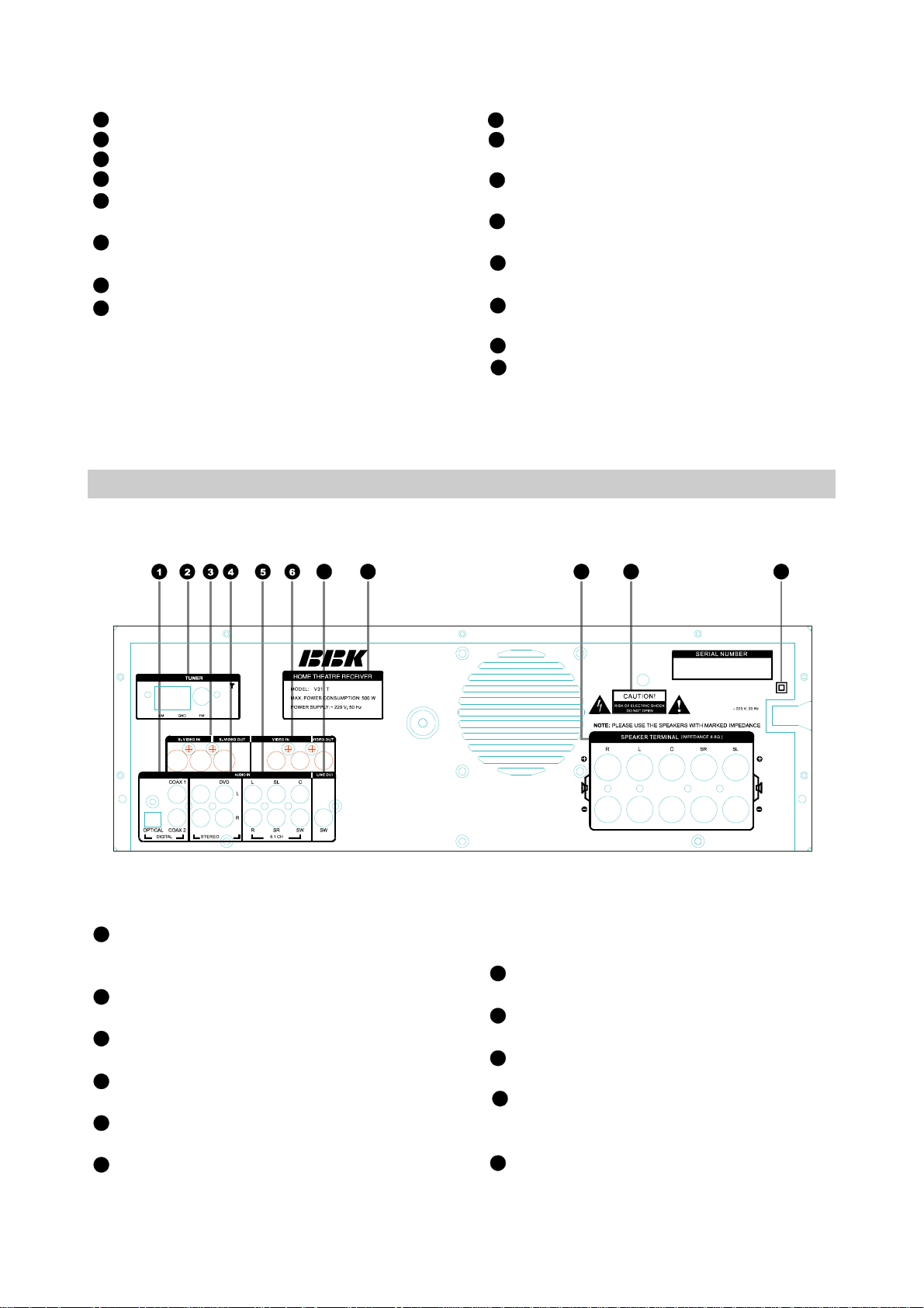
REARPANELILLUSTRATIONS
2.2ControlbuttonLocationsandExpLanations
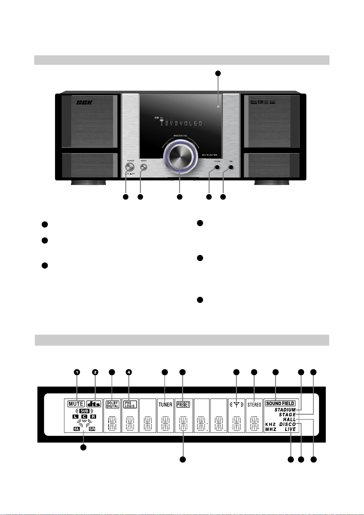
2.2.1Frontpanelfunctionsandillustrations
6
HOMETHEATRERECEIVERAV311T
MUTE
SL
1 2 4 53
1
POWERswitch
Switchon/offtheACpoweroftheunit
2
MENUbutton
MENUbutton,pleaserefertotherelated
chaptersfordetails
3
Multi-FunctionKnob
Innormalworkingmode,synchronously
adjust6-channellevel.Inaddition,by
usingthisknobandMENUbutton,you
mayfulfilmultiplefunctions.Pleaserefer
totherelatedchaptersfordetails...
PRESET
TUNER
STERO
MP3
RCL
SR
SLEEP
SOUNDFIELD
STEREO
STADIUM
DIGITAL
OPTICAL
STAGE
CH HALL
KHZ
DISCO
MHZ
LIVE
4
Headphonejack
5
MICjack
6
IRsensorwindow
Receivetheremotecontrolsignals.
2.2.2VFDDISPLAY
3 11
16
85 76 9 10
1314 1215
-5-
Page 11
1
MUTEsymbol
2
DTSdecodemodesymbol
3
DolbyDigitaldecodemodesymbol
4
DolbyProLogicdecodemodesymbol
5
TUNERsymbol,itsflickershowsthetuneris
Ⅱ
insignalsearchingstate
6
Callthepresetsavedradiostation,orhas
savedthecurrentlytuningchannel
7
Thetunerhasreceivedsignal
Stereodecodemodeorthecurrently
8
receivedFMradiostationisstereooutput
signal
2.2.3REARPANELILLUSTRATIONS
9
DSPdecodemodesymbol
10
InDSPdecodemode,stimulateSTADIUM
soundfield
11
InDSPdecodemode,stimulateSTAGE
soundfield
12
InDSPdecodemode,stimulateHALLsound
field
13
InDSPdecodemode,stimulateDISCO
soundfield
14
InDSPdecodemode,stimulateLIVEsound
field
15
Connectchannel,dataformatdisplayarea
16
Effectivechanneldisplayarea
8
7
1
1
DIGITAL
VCD
VCD
VCDDVD DVDOUT OUT
Coaxialdigitalsoundsourceinputjack1,2;
opticaldigitalsoundsourceinputjack
2
AM/FMantennaterminal
ConnectAM/FMantennaoutside
3
S-VIDEO
VCDDVDS-VideoSelectedJacks
、
4
STEREO
VCDDVDstereoaudiosignalinputjack
、
5
5.1CH
5.1CHaudiosignalinputjack
6
VIDEO
VCDDVDVideoSelectedJacks
、
10
7
LINEOUT
9
Subwoofersignallineoutputjack
8
Data
Modeldataplate
9
Speakerjack
Connectwithspeakerterminals
10
CAUTIONmark
Remindtheuserofdangerousvoltage
Inside
11
Dualsquaresymbol
ClassIIelectricshockprotectionproduct
11
-6-
Page 12
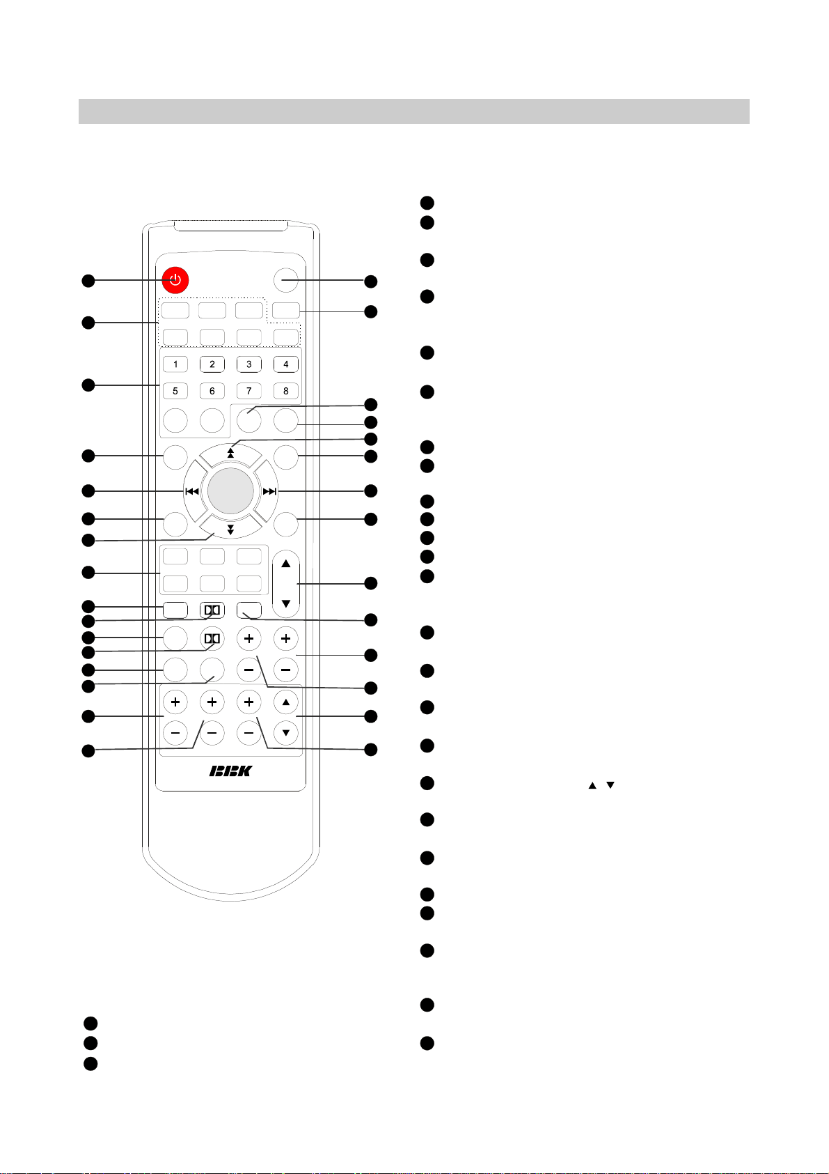
2.2.4ILLUSTRATIONSTOTHEREMOTECONTROL
1
STANDBYbutton:Enterorexitstandbystate
2
SOUND/VIDEOSOURCEbutton:Selectinput
signalsourcesmanually
3
NUMBERbuttons:Forsavingandcallingsaved
radiostations
4
AMSTEPbutton:Pressingthisbuttonforlong
(above3seconds)mayswitchstepvalus9KHz
or10KHzintheAMwaveband
5
FORWARD/AFTERWARDbutton:Callthe
savedradiostationsforward/backward
6
DEFAULTbutton:Pressthisbuttonforlong
(above3seconds),theunitautomatically
restoressystemparametertodefaultvalue
7
MULTI-FUNCTIONbuttons
8
CHANNELbuttons:Usingwithmulti-function
buttonsmayseparatelyadjust channelleve
9
STEREOMODEbuttonl
10
DOLBYPROLOGICDECODEMODEbutton
11
DTSDECODEMODEbutton
12
DOLBYDIGITALDECODEMODEbutton
13
SPEAKERMODESETUPbutton:Pressingthis
buttonmaycircularlyselectmainspeakermode
andsubwooferon/offmode
14
EQMODEbutton:Pressthisbuttonto
circularlyselectEQmode
15
KARAOKEECHO(+,-)button:AdjustKaraoke
echo
16
KARAOKETREBLE(+,-)button:Adjust
Karaoketreble
17
KARAOKEBASS(+,-)button:AdjustKaraoke
bass
18
KARAOKEVOLUME()button:Adjust
Karaokevolume
19
MAINCHANNELTREBLE(+,-)button:Adjust
mainchanneltreble
20
MAINCHANNELBASS(+,-)button:Adjust
mainchannelbass
21
DSPDECODEMODEbutton
22
MAINVOLUMEbutton:Capableof
synchronouslyadjusting6-channelvolume
23
DELAYbutton:Usingwithmulti-function
adjustmentbuttonsmayadjustcentre,surround
channeldelay
24
FMSTEREOMODEbutton:Manually/
automaticallyselectFMstereomode
25
WAVEBANDbutton:UsedtoswitchFM/AM
waveband
TUNER
MEM
RC
TREBLE
MUTE
TEST
5.1CH
BAND
MODE
DELAY
VOL
BASS
MICVOL
STANDBY
1
OPTICAL
2
3
4
5 5
66
7
8
9
10
11
12
13
14
15
16
26
MEMORYbutton:Savetuningstations
27
NOISETESTINGbutton
28
MUTEbutton
COAX.1 COAX.2
DVD
VCD
9 0
STEP
DEFAULT
L
SL SW SR
STEREO DSPPLⅡ
DIGITAL
DTS
EQMODE
SPK.
ECHO TREBLE BASS
KARAOKE
RC-311
28
27
26
25
7
24
23
22
21
20
19
18
17
Ⅱ
、
-7-
Page 13
2.3BASICOPERATIONS
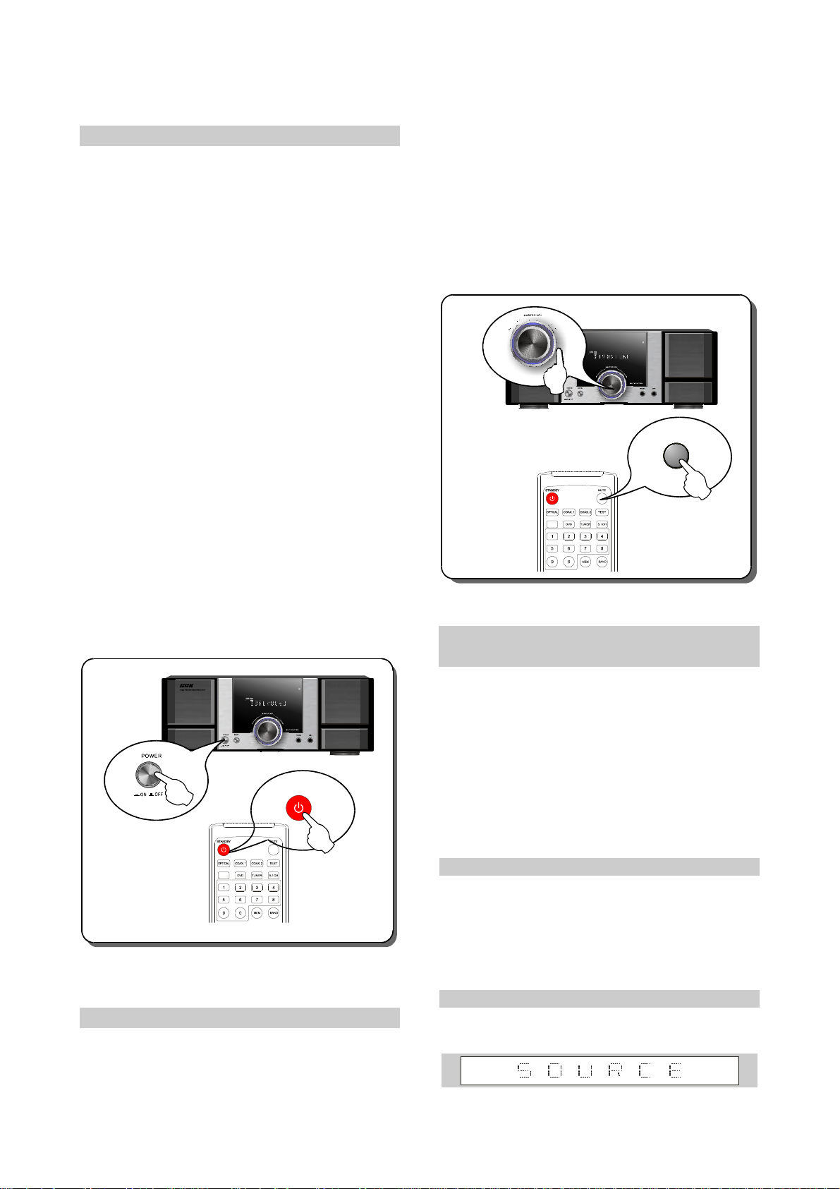
2.3.1TurnOn/OfftheUnit
1.PowerOn
◆
Beforepoweron,pleasecheckwhetherthe
poweraccordswiththemarkedspecsofthe
unit,whetherthepowersocketaccords
withthepowerplugoftheunitandwhether
thesoundsourceconnectioncords,output
cordsarecorrectlyconnected.Thenyoumay
connectthepower;
◆
PressPOWERswitchonthefrontpanelofthe
unitandtheindicatorlightonthepanelflickers
Theunitautomaticallyconnectwiththeinput
soundsourcebeforepower-offlasttime,and
automaticallyselectdecodemodeaccording
totheinputsoundsourceformat.
2.Standby
◆
Iftheuserwantstofinishingoperatingina
shorttime,youmaypressSTANDBYbutton
ontheremotecontroltoenterstandbystate.If
youwanttooperateitagain,pressSTANDBY
buttonagaintoexitstandbystate.
3.PowerOff
◆
Ifnotgoingtouseforalongperiod,press
POWERswitchonthefrontpaneltoturnoff
thepower,andtheindicatorlightturnsout.
theVFDscreenislightened.Inmutestate,
pressMUTEbuttonontheremotecontrol,the
unitrestorestooutputsoundandthe"MUTE"
symbolturnsout.UsingtheMULTIFUNCTION
knobonthefrontpanelorpressingMAIN
VOLUMEbuttonontheremotecontrolmay
alsocancelmute.
MUTE
SL
VCD
SOUNDFIELD
STEREO
PRESET
TUNER
STERO
STADIUM
MP3
DIGITAL
OPTICAL
SLEEP
RCL
SR
STAGE
CH
HALL
DISCO
KHZ
MHZ
LIVE
MUTE
Mute
MUTE
SL
VCD
SOUNDFIELD
STEREO
PRESET
TUNER
STERO
STADIUM
DIGITAL
OPTICAL
MP3
SLEEP
RCL
SR
STAGE
CH HALL
KHZ
DISCO
MHZ
LIVE
STANDBY
TurnOn/Off
theUnit
2.3.2Mute
◆Innormalworkingstate,pressMUTEbutton
ontheremotecontrol,
"MUTE"symbolonthetopleftcornerof
theunitissilentandthe
2.3.3SelectInputSoundSourceand
VideoSource
◆Thisunithas1-wayopticalinputterminal,2waycoaxialinputterminal,1-wayVCDinput
terminal,1-wayDVDinputterminaland5.1CH
inputterminal.Youmayusetheremotecontrol
todirectlyselectinputsoundsource,oruse
MENUbuttonandMULTI-FUNCTIONknobon
thefrontpaneltoselectinputsoundsource
throughmenu.Youarerecommendedtouse
remotecontrolmeans.
RemoteControlMeans
◆PresstheSOUNDSOURCEbuttononthe
remotecontroltoseparatelyselectthesound
sourceofoptical,coaxial1,coaxial2,VCDand
DVDastheworkingsoundsourceofthisunit.
PressTUNERbuttontoselectthebuilt-ituner
ofthisunitastheworkingsoundsource.
MenuMeans
◆PressMENUbuttononthefrontpanelofthe
unitandVFDscreendisplays"SOURCE".
-8-
Page 14
◆
RotatetheMULTI-FUNCTIONknob,VFD
screenwilldisplay"OPTICAL","COAX1",
"COAX2","DVD","VCD","EXT5.1CH",
"AM"and"FM"symbolswhichrespectively
standsforthesoundsourcesonoptical,
coaxial1,coaxial2,DVD,VCDandexternal
5.1CHterminals,andthebuilt-inAM,FMwave
bandsignals.PressMULTI-FUNCTIONknob
toselectthissoundsource.
Selectvideo
◆
WhenTunerin,Novideoout;WhenVCDAudio
in,theVCDvideoisselected;WhenDVD
、、
audio5.1CHCOAXIALandOpticalin,The
DVDvideoisselected.
SOUNDFIELD
STEREO
PRESET
TUNER
STERO
STADIUM
DIGITAL
OPTICAL
MP3
SLEEP
RCL
SR
STAGE
CH HALL
KHZ
DISCO
MHZ
LIVE
SelectSource
OPTICAL
COAX.1 COAX.2
MUTE
SL
VCD
5.1CHTUNERDVDVCD
Inputchannel PLII
Analog
Signal
Digital
Signal
(from
2/0AC-3 Yes Yes Yes No No
Optical,
Coax1,
Coax2)
Stero
DVD
Yes Yes No No Yes Stereo
VCD Yes Yes No No Yes Stereo
PCM Yes Yes No No Yes Stereo
AC-3 Yes No Yes No No
DTS Yes No No Yes No DTS
NOTE:InDolbyProLogicdecodemode,itis
Dolby
Digital
Ⅱ
DTS DSP
Default
Decode
Dolby
Digital
Dolby
Digital
effectiveonlywhensamplingrateless
than96KHz.
ThisunitcanonlyreceivePCMsignalswith
samplingratelessthan96KHz.Therearetwo
meansofmanuallyselectingdecodemode:
Remotecontrolandmenu.
RemoteControlMeans
PressSTEREO,II,DSP,DTS,DIGITAL
◆
buttonsontheremotecontrol,ifthedecode
modethatyouselectedcannotberealizedto
inputsignal,thesystemstillremainsthe
Originaldecodemode.
MenuMeans
PressMENUbuttononthefrontpanel
◆
continuouslyuntilDECODEappears.Rotate
theMULTI-FUNCTIONknob,andVFDscreen
willdisplay"STEREO,DSP,DOLBY,PROII,
DolbyDigital,DTS",whichstandsforSTEREO,
DSP,DolbyProLogicII,DolbyDigitalandDTS
decodemoderespectively.Youneedtopress
theMULTI-FUNCTIONknobtoconfirmto
enternewdecodemode.
Note:Asforacertaininputchannel,ifsome
decodemodesdonotexist,theoperation
isinvalid.
2.3.4SelectDecodeMode
◆ThisunithasDolbyDigital,DolbyProII,DTS,
DSPandSTEREOdecodemodes,butnot
everyinputchannelhasallthedecodemodes.
Whentheuserswitchestheinputchannelor
changestheinputsignalformat,theunitmay
automaticallyselectthedefaultdecodemode
accordingtotheinputsignalformat.Certainly,
theusermayalsoselectthedecodemode
manually,andpleaserefertothefollowing
tablefortheselecteddecodemodeofeach
channelandthedefaultdecodemode.
Table1:Relationbetweeninputchanneland
decodemode
-9-
HOMETHEATRERECEIVERAV311T
MUTE
SOUNDFIELD
STEREO
PRESET
TUNER
STERO
STADIUM
DIGITAL
MP3
OPTICAL
SLEEP
STAGE
RCL
CH HALL
KHZ
SL
DISCO
SR
MHZ
LIVE
SelectDecodeMode
Page 15
2.3.5AdjustVolume
◆RotatingtheMULTI-FUNCTIONknobonthe
frontpanelorpressingtheMAINVOLUME
buttonontheremotecontrolmay
synchronouslyadjust6-channellevelandthe
screendisplays"VOLXX"adjustmentrange
0~60.
Note:Themainvolumeautomaticallysetsin20
eachtimewhenpoweron.
AdjustChannelLevel
HOMETHEATRERECEIVERAV311T
MUTE
SL
SOUNDFIELD
STEREO
PRESET
TUNER
STERO
STADIUM
MP3
DIGITAL
OPTICAL
SLEEP
MASTER
VOL
STAGE
CH
HALL
KHZ
DISCO
MHZ
LIVE
RCL
SR
AdjustVolume
2.3.6AdjustChannelLevel
◆◆PressCHANNELbuttonontheremotecontrol
andtheVFDscreendisplaysthe
correspondingchannelsymbol:"FLXXX,FR
XXX,FCXXX,SLXXX,SRXXX,SWXXX",
whichmeansleftchannel,rightchannel,
centrechannel,surroundleftchannel,right
surroundchannelandsubwooferchannel
respectively.
PresstheMULTI-FUNCTIONadjustment
buttonontheremotecontroltoadjustchannel
level.Theadjustmentrangeofchannellevelis
-60~+60
Figure:Thedesignofchannellevelonthescreen
2.3.7AdjustMainChannelTone
◆PressTREBLEandBASSbuttonofmain
channelontheremotecontroltoadjustthe
mainchanneltrebleandbass
respectively.
TREBLE BASS
AdjustMainChannelTone
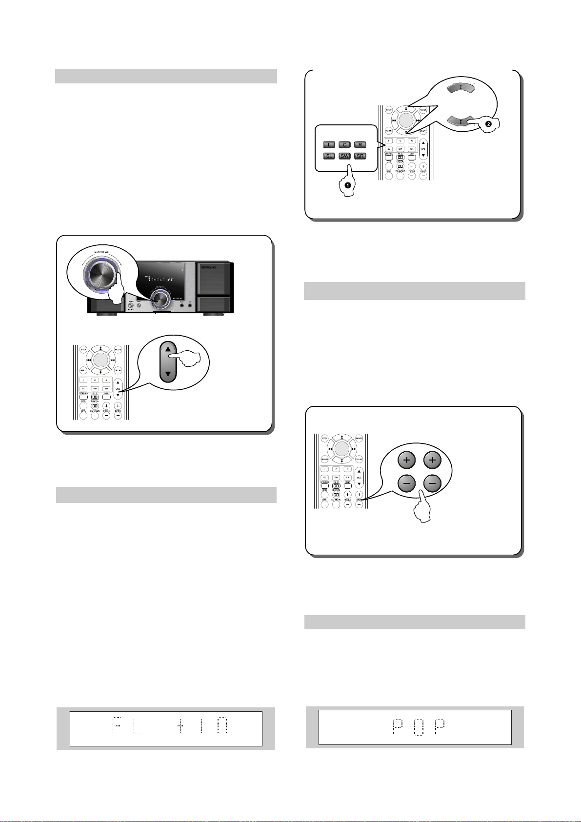
2.3.8SelectEQMode
◆PressingEQbuttonontheremotecontrolmay
selectFLAT,DISCO,POP,ROCKandJAZZ
moderespectively.Figure:EQmodedisplay
-10-
Page 16
EQMODE
SelectEQMode
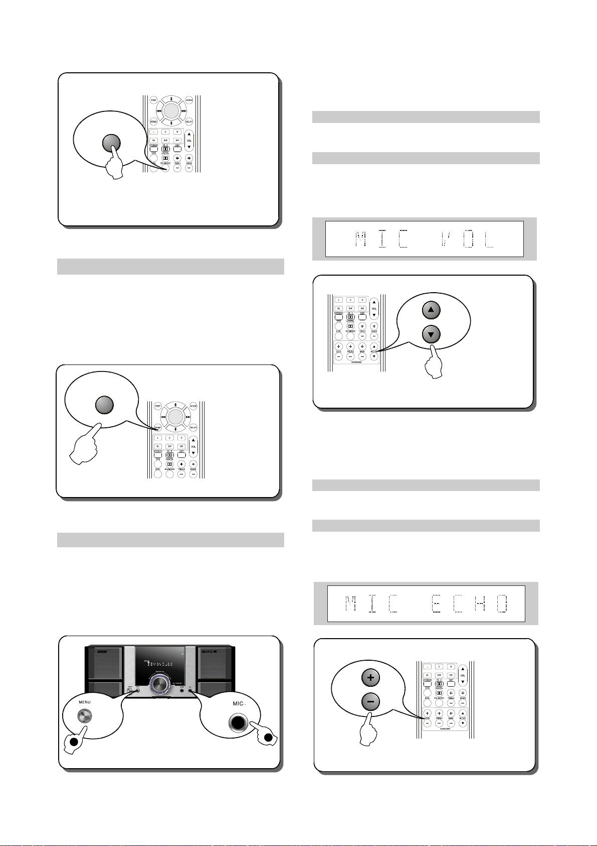
2.3.9DEFAULT
PressDEFAULTbuttonforlong(above3
seconds),andtheunitrestoresthechannel
levelandKaraokevolumeparameterstodefault
Parameters.
1.Karaokevolume
TherearetwomeanstoadjustKaraoke
◆
volume:remotecontrolandmenu.
RemoteControlMeans
PressKARAOKEVOLUMEbuttononthe
Remotecontrol
MenuMeans
PressMENUbuttononthefrontpaneluntil
MICVOLappears,andthenrotatetheMULTIFUNCTIONknob.
MICVOL
DEFAULT
Calldefaultparameter
2.3.10Karaoke
InsertthemicrophoneintotheMICjackon
thefrontpanelandpushtheMICswitchtoON(if
thereisswitch).Keepanappropriatedistance
Withspeakertoavoidwhistle.
HOMETHEATRERECEIVERAV311T
MUTE
SL
SOUNDFIELD
STEREO
PRESET
TUNER
STERO
STADIUM
DIGITAL
OPTICAL
MP3
SLEEP
RCL
SR
STAGE
CH HALL
DISCO
KHZ
LIVE
MHZ
Karaokevolume
2.Karaokeecho
TherearetwomeanstoadjustKaraokeecho:
◆
remotecontrolandmenu.
RemoteControlMeans
PressKARAOKEECHObuttonontheremote
control.
MenuMeans
PressMENUbuttononthefrontpaneluntil
MICECHOappears,andthenrotatetheMULTIFUNCTIONknob.
ECHO
2
MenuandMICjack
1
Karaokeecho
-11-
Page 17
3.Karaoketone
◆PressTREBLEandBASSbuttonofKaraoke
ontheremotecontroltoadjustKaraoketreble
andbass.
After3secondssearchingradiostation,you
mayrotatetheMULTI-FUNCTIONknobto
Adjustvolume.
TREBLE BASS
Karaoketone
BASICOPERATIONS
2.3.11Tuning
Beforetuningoperation,pleaseselect
appropriatewavebandaccordingtothe
Followingsteps.
PressTUNERbuttonofsoundsource
◆
selectionontheremotecontrol;
PressBANDbuttonontheremotecontrolto
◆
selectwavebandordirectlyenterthetuning
FM,AMwavebandthroughmenu.1.Auto
search
RemoteControlMeans
PresstheMULTI-FUNCTIONbuttonforlong
◆
(above1second),andtheunitwill
automaticallysearchradiostationsforwardor
afterward.Untilradiostationwithstrong
signalissearched,itwillautomaticallystop.
PresstheMULTI-FUNCTIONbuttontofine
◆
adjustifnecessary.
MenuMeans
PressMENUbuttononthefrontpaneluntil
◆
VFDscreendisplays"TUNSEEK".
VCD
TUNER
TUNER
2.Autosearchandsaveradiostation
◆◆PressMEMORYbuttonontheremotecontrol
untilVFDscreendisplays"MEMORY".
PressMULTI-FUNCTIONbuttonforlong
(above1seconds),theunitwillautomatically
searchradiostationforwardorbackwardand
thenautomaticallysaveit.Thisunitmay
automaticallysave36FMand12AMradio
stations.
BAND
VCD
◆RotatetheMULTI-FUNCTIONknobandthe
unitwillautomaticallystopaftersearchingthe
radiostationwithenoughstrongsignal. Within
about3seconds,youmaycontinuerotating
theknobandsearchingradiostation.
BAND
3.Saveradiostationmanually
◆PressMEMORYbuttonontheremotecontrol
andthenNUMBERbuttonstosaveradio
station.Ifthesavedradiostationnumberis
over9,pleasepress2numberscontinuously.
-12-
Page 18
◆Aftercompletelysaving,PRESETsymbolon
thescreenislightened.
HOMETHEATRERECEIVERAV311T
1
MUTE
SL
SOUNDFIELD
STEREO
PRESET
TUNER
STERO
STADIUM
DIGITAL
OPTICAL
MP3
SLEEP
RCL
SR
STAGE
CH HALL
DISCO
KHZ
MHZ
LIVE
MULTI-FUNCTIONknob
2
TheExplanationofMODEbutton
Thisunithastwoworkingmodesinthe
Receivingstatus:
AUTO/MANUAL
1InAUTOworkingmode,ifyouselectFM
、
Waveband,thisunitwillautomatically
recognizetheradiostationprogramismono
signalorstereosignalandkeepthemonoor
stereoReceivingstatus.
2Ifthereceivedradiostationprogramhas
、
Loudernoiseorcacophonyinstereostatus,
youmayswitchtoMANUALworkingmode.In
thisway,theunitisinmonoreceivingstatus
todecreasenoiseandcacophony
generally.Youmayswitchthetwoworking
modesthroughMODEbuttonontheremote
control.
4.Callthesavedradiostation
◆
PressNUMBERbuttonstocallthesavedradio
stationdirectly.
◆
PressFORWARD/BACKWARDbuttonstocall
thesavedradiostation.Calltheformeror
behindoneofthesavedradiostation.
◆
Aftercompletelycalling,"PRESET"symbolon
theVFDscreenislightened.
5.SelectAMstepvalue
◆
PressingAMSTEPbuttonforlong(above3
seconds)mayswitchtheAMstepfrequency
value,thatis,whentuningthestepvalueeach
timeis9KHzor10KHz.
MEM
Remotecontrol
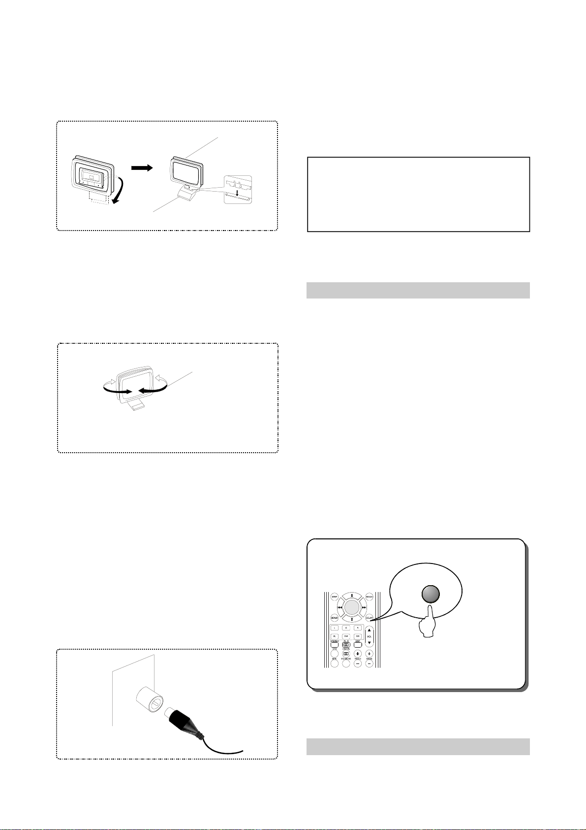
AntennaConnection
YoumayuseouraccessionalAMandFM
indoorantennawheninbadreceivingeffect.
Generallyspeaking,theseantennaecansupply
enoughsignalstrength.
ConnecttoAMRoundAntenna
1Pushthejackbuttontoopenit.
、
2ConnecttheAMroundantennacordtoAM
、
ANTandGNDterminals.
3Letgooffthebuttontoclampthespeaker
、
cord.Pullthecordlightlytocheckthe
connectionIsrightornot.
VCD
Callthesavedradiostation
2.3.12Tuning(Continued)
-13-
HowtoConnect
Pushthejackbuttontoopenit.
1
3
2
1
Insertthespeakercord.
2
Letgooffthebuttontoclamp
3
thespeakercord.
Page 19
4ConnecttheAMroundantennatothestand.、
4
AMroundantenna
Stand
5
5AdjustthedirectionofAMroundantennato
、
getthebestreceivingeffect.
Rotate
NOTE:
DonotusetheoutdoorandindoorFM
Antennaeatthesametime.
GND(Grounding)terminal
Inordertoensurethesafetyanddecreasethe
interference,pleasewellconnecttheGNDterminal.
Thebettergroundingmethodisinsertthemetalpole
intowetground.
2.3.13ChannelDelay
◆
Channeldelayoperationisonlyavailablein
DolbyDigital,DTSandDolbyProLogicII
modes.
◆
PressDELAYbuttonontheremotecontrol.
WhenVFDscreendisplays"CXXMS",use
MULTI-FUNCTIONbuttontoadjustthecentre
channeldelay.Theadjustmentrangeis0~5ms
◆
PressDELAYbuttonontheremotecontrol
again.WhenVFDscreendisplays"SXXMS",
useMULTI-FUNCTIONbuttontoadjustthe
surroundchanneldelay.Theadjustmentrange
is0~15msinDTSandDolbyDigitaldecode
modes,and15~30msinDolbyProLogicII
decodemode.
NOTE:
1AMroundantennashouldbeplacedfaraway
、
fromtheequipment.Youmayputuponthe
walloronthebookshelf.
2AMroundantennaandoutdoorantennacan
、
beusedatthesametime.
ConnecttoFMAntenna
ConnecttotheindoorFMantenna
ConnecttheaccessionalindoorFMantenna
to75UNBAL.FMANTterminal.
Ω
DELAY
Channeldelay
2.3.14NoiseTesting
-14-
Page 20
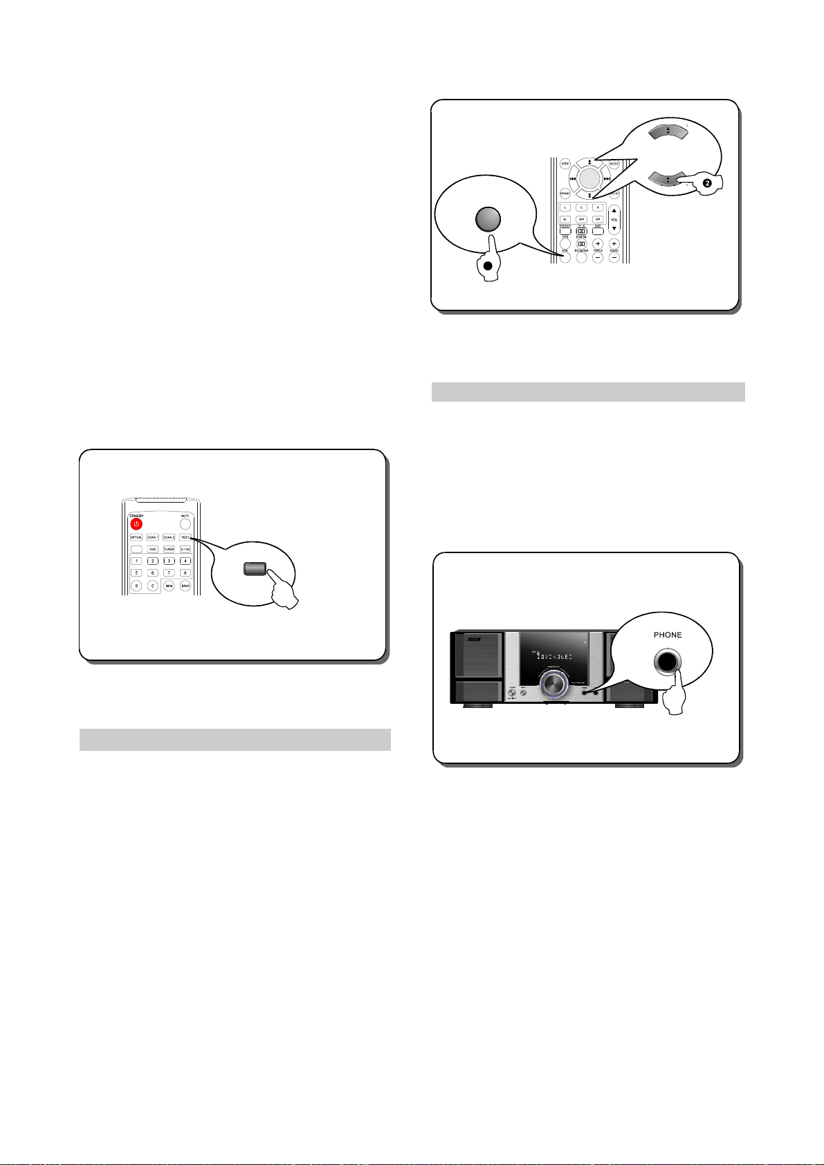
◆◆Duringsystemworking,itisusedforusersto
adjustlevelbalancebetweenchannelsin
multi-channelstate.
Innon-STEREOdecodemode,pressTEST
buttonontheremotecontroltoenternoise
testingmode.Theunitwilloutputnoise
accordingtothesequenceofleft,centre,right,
surroundrigntandsurroundleft.Thelasting
periodofeachchannelis2s,duringwhich
timeusersmaypresstheMAINVOLUME
buttonontheremotecontroltosynchronously
adjust6-channellevel,andmayalsopress
MULTI-FUNCTIONbuttontoadjusteach
cnahhel'slevel.Toexitnoisetestingmode,
pleasepressTEST buttonagain.
SPK.
1
Selectspeakermode
2.3.16Headphone
◆Thisunitiswithindividualheadphoneamplifier.
Ifnecessary,pleaseinserttheheadphoneplug
intotheheadphonejackonthefrontpanel.In
thisstate,changingdecodemodeisinvalid.
VCD
TEST
Noisetesting
2.3.15SelectSpeakerMode
◆PressSPEAKERMODESETUPbuttononthe
remotecontrol,when"SPSMALL"or”SP
LARGE"appears,pressingMULTI-FUNCTION
buttonagainmaychangetheleft/rightspeaker
mode.Pressspeakermodebuttononthe
remotecontrol,when"SUBON"or"SUBOFF"
appears,pressingMULTI-FUNCTIONbutton
againmaysetwhetherthereissubwoofer
speakermode.
Note:Theselectionof"Large"or"Small"isset
byspeakercalibraterandbassplaying
ability.Whensubwooferspeakerand
subwooferoutputterminalareconnected,
youmayset"SUBON",orelse,"SUB
OFF".Whenspeakermodeissetin
"SMALL",subwooferspeakermustbeset
in"ON".
HOMETHEATRERECEIVERAV311T
MUTE
SL
SOUNDFIELD
STEREO
PRESET
TUNER
STERO
STADIUM
DIGITAL
MP3
OPTICAL
SLEEP
RCL
SR
STAGE
CH HALL
DISCO
KHZ
MHZ
LIVE
Headphone
-15-
Page 21

2.4ACCESSORIES
UserManual
◆
RemoteControl
◆
AVCord
◆
◆
◆
◆
◆
''
Jacktomini-jackadapter
#
7AAAbattery
Warrantycard
FM/AMantenna
1pcs
1pcs
1pcs
1pcs
2pcs
1pcs
1suit
2.5SPECIFICATIONS
1RatedOutputPower
、
MainChannel(1kHz/4,RMS,TotalHarmonicDistortion1%):80W+80W
CentreChannel(1kHz/4,RMS,TotalHarmonicDistortion1%):15W
SurroundChannel(1kHz/4,RMS,TotalHarmonicDistortion1%):15W+15W
2Separability(1kHz,RatedCondition):
、≥
3TotalHarmonicDistortion(1kHz,RatedCondition):
、≤
4EffectiveFrequencyRangeunderLimitedGains(NormalWorkingCondition):
、
MainChannel20Hz~20kHzdB
Centre/SurroundChannel20Hz~20kHzdB
5Signal-to-NoiseRatio
、
MainChannel(Input600Short-Circuit,Aweighted):80dB
CentreChannel(Input600Shout-Circuit,Aweighted):73dB
SurroundChannel(Input600Shout-Ciucuit,Aweighted):73dB
6TUNER
、
Frequencyrange:FM:65-74MHz,87-108MHz
7InputSensitivity(RatedCondition)
、≤
8LoadImpedance
、Ω
POWER
1PowerSupply:~220V1050Hz
、±%
2MaximumPowerConsumption:500W
、
OTHERS
1NetWeight:About8kg
、
2Dimensions:420337135mm
、××
Ω≤
Ω≤
Ω≤
40dB
0.7%
+1
-3
+1
-3
Ω≥
Ω≥
Ω≥
AM:500-1611KHz(9KSTEP)
520-1710KHz(10KSTEP)
100mV
A114~8
-16-
Page 22

ChapterThreeUnitCircuitPrinciple
SectionOnePrincipleoftheplayer
AV311T(RU)isanadvancedpoweramplifierlaunchedintomarketrecently.ItiswithDTS/AC-3
digitaldecodefunction,whichmakessoundprocessingmoreperfecttoeffectivelycontrolthedistortion
andnoiseinthecourseofaudiosignal.
3.1.1Compositionoftheplayer
1.Signalprocessingboard:gating,frontstageamplifyingofsignalandfrontstageprocessingof
Karaokesignal.
3.Controlpanel:VFDdisplay,menubuttonandmainvolumecontrol.
4.Powerboard:providevoltagerequiredbyeachunitcircuit,andperformtheplayerprotection
function.
5.Poweramplifierboard:poweramplifyingof5.2CHsignaloranalogsignal.
6.Headphoneboard:Karaokeinputandheadphoneoutputsignalamplifying.
7.Videboard:input/outputswitchoftwo-channelcompositevideoandS-videovideosignal.
3.1.2Functionandfeatures
Simpleoperationpanelinterface;thepaneloftheplayerhasonlyonepowerswitchbutton,menu
◆
buttonandalargeknob,simpleandclear;
◆
WirhDTS/AC-3decodefunction;
◆
Optical,coaxialsignaldecodefunction;
◆
Built-in5-channelpoweramplifying,adaptabletoAC-3/DTSandstereomusicreplay.Main
channel110W.Centre/surround22Wwithpowerfulpower;
◆
With6-channelvolumecontrolandseparatelevelcontrol,andalsowith7-bandelectronic
equalization;
◆
WithmultipleelectronicEQmodes,adaptabletodifferentmusicalstyles;
◆
Digitalsoundfielddelayfunction;
◆
Withtuningfunction;
◆
Withintelligentprotectionofover-currentandover-voltage
◆
Karaokefunctionandheadphoneoutput;
-17-
Page 23
220V
Signaloutput
Xs1
Xl100
Powerboard
Transformerentry-level
Xs2
SWITCH
Xs3
Xs4
SWM
RLY0
P_RC
OVER
VC+
GND
GND
Secondarycoil
Secondarycoil
L2
R2
C2
Sl2
Sr2
VC-
~8.5V
GND
~8.5V
+12V
GND
-12V
RLY
P_RC
P_LRM
P_CSM
SWM
L1
R1
C1
Sl1
Sr1
D+5V
DGND
L1
R1
PH_SW
GND
MIC
Videoboard
xs101
xp20
Xs100
Xs22
Xs101
Signalboard
Xp17Xp16
Xs16
Xs17
Decodeboard
RDSoutlet
Xp14
Xs14
LAT
CE
CLK
DATA
DO
P_DIST
OK_DAT
OK_CLK
P_KT
REM
DST
DCK
DDA
Transformer
Xp25
Micorearphoneboard
Viewboard
+5VD
GND
RLYC
NC
DDA
DCK
DST
FAN
REMMOTE
Page 24
DIGITALAUDIOINPUT
VCD
DVD
5.1CH
VCD
DVD
VCD
DVD
VIDEOBOARD
1
2
3
4
5
6
TUNER
6
6
6
Digital
audio
L
R
L
R
CD4052
CD4052
1
2
3
1
2
3
4052-A/4052-B
2*COAXIAL/OPTICAL
L/R
4052*2
L/R
5.1CH(L/R/SL/SR/C/SW)
OK_CLK/OK_DATA
9
8
7
6
5
4
3
2
1
L/R
DO/CLK/DAT/CE
4558_B
4558_A
+5V
PH_SW
PH_L
PH_R
Dual-decodeIC,
CPU
CPU
PT2315
MIC_VOL
TONE
ECHO
adjustment
Amplify
LM4880
P_DISP
Straightthrough
ECHO
PT2399
CPUI/O:
INPUTSET
5.1CH
4053_INT
L/R/SL/SR/C/SW
CLK/DAT/LAT
TUN_L/TUN_R
REMOTE
DCL/DDA/DST
DISPLAYBOARD
2*LED
PT6311
Mix&buffer
4558
Echovolume
CLK/DATA/LATDO/CE
OK-CLK/OK-DATAP-KT
DCL/DDA/DATAREMOTE
P-LRM/P-SCMP-RLYP-DISP
KM
0_LEVEL
2*KEY
VFD
FUNVOL
REMOTE
6311I/O:
62446I/O:
VOL&TONE
M62446
FAN
SL/SR
L/R
C
SW
KM
FAN
TUN-L/TUN-R
FANRLYC
4052-A/4052-B
5.1CH4053-INT
Mix&buffer
4558
Mix&buffer
5532
Mix&buffer
4558
+12V
AGND
Power
-12V
+6.8V
~VS
~VS
+5V
P_LRM/P_SCM
SW_OUT
+6.8V
AGND
-6.8V
+5V
+5VD
Load
detect
Vc+
AGND
Vc-
AMPBOARD
L
R
C
SL
SR
Relaydrive
RLYC
Mainpower
amplifierboard
power
POWERBOARD
Preposition
power
NGD
Vs-
Vs+
Central
surround
power
SWmuteandrelay
statedetect
L
R
C
SL
SR
MICPHONEBOARD、
Page 25
SectionTwoUnitCircuitPrinciple
3.2.1Signalprocessingboard
1.Inputselectioncircuit
AV321T(RU)has6kindsofinputmeansinall:opticalinput,coaxialinput,CD,DVD,5.1CHand
tuninginput.Digitalsignalsofoptical,coaxialinputofthisplayeraredirectlysenttopoweramplifier
boardforprocessingthroughflatcable.AnaloginputselectionofAV321T(RU)isfulfilledthroughan
electronicswitchCd4052(N101)anditstruthvaluetableisshownasthefollowing:
Estate
状态
PIN
引脚
A 1 0 1
B 1 1 0
AV321T(RU)has3kindsofinputstates:tuning,VCD,DVD,andtheyarecontrolledthrough4052-
A,4052-Bsignalrespectively(refertotruthvaluefordetails).Signalsafterbeinggatedoutputfrompin3
VCD DVD
Tuning
andpin13ofN101,andthenoutputleft/rightmainchannelsignalfromitspin1,12throughN111CD
4052todecodeboardforsignalprocessing.
Analogsignalinputin5.1state:thegatingof5.1analogsignalinputofAV321T(RU)iscontrolledby
twoICCD4053(N102,N103),controlpin9,10,11ofCD4053areallcontrolledbythe5.1CHsignal
outputtedfrompin4ofM62446(N104),when5.1CHsignalishighlevel,thegatingisanalogsignalinput
of5.1state;inthisstate,thereisnodigitalsoundfield,allsignalsarestraightthrough;when5.1CHis
lowlevel,thegatingisthesynthesizedsignalafterdecoding.
Straightthroughanddigitalsoundfieldswitchcontrol:AV321T(RU)hastwodifferentmodesof
straightthroughanddigitalsoundfield,anditsgatinginputiscontrolledbyN111/CD4052andN102/CD.
Whencontrolsignal4053-INTishighlevel,foritisconnectedtotheenabledendofN102,thisICisin
nonworkingstate,mainchannelsignalsoutputthroughpin5,11ofN111anddirectlysendtoM62446
forprocessingtooutputHi-Fimusicalsignals.When4053-INTislowlevel,mainchannelsignalsare
senttodecodeboardfordigitalsoundfieldprocessingthroughXp17,andN102isalsoinworkingstate.
2.Karaokesignalprocessingcircuit
ForkaraokesignalssentfromMICbaseboard,aftercouplingandamplifying,onepathissentto
volumeandtoneadjustmentICPT2315(N203)forprocessing,thenafterechoanddelayadjustment
- 20 -
Page 26

throughPT2399(N204),itissenttopoweramplifierboardforsmallsignalamplifyingthroughbandPassfilter.PT2315iscontrolledbyMCU,sousersmayadjusthisdesiredKaraokeeffectatwillthrough
remotecontroller.
Anotherpathsignal,afteramplifyingrectification,controlsaswitchtriodeV2019014tocontrolthe
high/lowlevelofdetectsignalP-KTtofulfilthedetectingofKaraokesignals.WhentheinputtedKaraoke
signalislargeenough,theDCafterbeingrectifiedmakestriodeV201onandthenpullsdownP-KT
signal,whichmeansthatthereisKaraokesignalinput.Now,KMcontrolsignalislowlevel,triodeV101
2N5401,V102S8050bothcutoff,KaraokesignalsenterICN107NE5532foramplifyingthrough
couplingcapacitorC147,C149,thentheyaresenttoleft/rightchannel;whenCPUcannotdetectsignals
inacertainperiod,P-KTishighlevel,nowKMcontrolsignalofCPUchangesintohighlevel,triode
V101,V102arebothontomakeKaraokesignalshortcircuittoground,systemmutesKaraoekpart
automaticallytopreventtheinfluencetosoundeffectcausedbynoise.
3.Fanstartingcircuit
Whenpoweramplifieriswithload,forpowerislargeandtemperatureriseishigh,thisplayer
adoptsfantoperformheatradiation.Whenvolumeismorethan45dB,FANsignalsentoutfromcontrol
paneN101changesintohighlevel,V1039014andV105S8050areontoformpowersupplyloopoffan.
Whentheconnectedloadisheadphone,controllinePH-SWishighlevel,V1049014isontopulldown
FANsignal,sonomatterhowisthevolumeofsystem,fanwillnotstartup.
3.2.2Decodeboard
Mainelementfunctionofdecodeboardisshownasfollows:
ICSM8958AC25P(N116):controlcoreofMCUsystem
◆
IC493264(N105):highperformancedigitalaudiodecoder,includingDOLBYdecode,DTS
◆
decodeandDSPprocessing
ICCS8415(N106):serialdigitalaudiosignalreceiver
◆
ICCS5340(N108):2-channelA/Dconverter
◆
ICCS4360(N107):6-chanelD/Aconverter
◆
IC24C02(N115):statememorizer
◆
IC74HC04(N101):6-channelphaseinverter
◆
ICBM1117-3.3(N109):3.3VvoltageregulatingIC,whichprovidespowerforCS8415,Cs4923
◆
Workingprinciple:foropticalandcoaxialsignals,afterbeingfilteredbyinductor,capacitor,
reshapedbyphaseinverter74HC04(N101),theyaresenttoserialaudiodigitalsignaltoreceivesignal
inputpin4,1214ofICCs8415(N106),thenconverseserial digitalaudiosignaltoPCMsignalthrough
thisIC,andoutputfrompin16(samplingspeedsignal),17(mainchannelclocksignal),18(audiodata
signal)ofthisICtopin25(samplingspeedcontrolsignal),pin26(clocksignal),22(PCMdatainputport
- 21 -
Page 27

1)ofdigitalaudiodecodeICCs493264(N105)fordataprocessing.
Analogsignalsofleft/rightchannelaresenttodecodeboardthroughflatcableXs17,afterfront
stagesmallsignalprocessing,thensenttopin10,12ofICCs5340(N108)forA/Dconversiontochange
analogaudiosignalintoPCMsignal,thensentfrompin4(audioPCMsignal),17(samplingspeed
signal),18(clocksignal)ofN108topin27,28,29ofN105,thatis,inputfromanotherPCMinputportof
N105fordataprocessing.
Therefore,digitalsoundfieldprocessingofanalogsignalandprocessingofcoaxial,opticalaudio
digitalsignalareseparate,ifonlyonepathworksabnormally,thepossibilitythatproblemappears
beforeN105islarge.
CS493264(N105)iswithpowerfuldigitalsoundfieldprocessingfunction,allDSPprocessing,Pro.
LogicIIprocessingandDOBLY/AC-3processingareallperformedinsideunderthecontrolof
MCU/SM8958AC25P(N116).
AudioPCMsignalafterbeingprocessedbyCS493264(N105)issenttoCS4360(N107)forD/A
conversiontorestorePCMsignalinto6-channelanalogsignal,thenfilterhighfrequencysignaloutside
therangeofaudiofrequencythroughaband-passfilter, thensenttoinputgatingpartforselectioninput.
Actedashecoreofthewholesystem,MCU/SM8958AC25P(N116)hasimportantfunction.All
controlsignalsaresentoutbyit,anditwilldetecteachdifferentsignalanduserorderatanytimeto
controlactionofeachpartofmachine.IfthisIChastrouble,theplayerwillbenotabletoworknormally.
Inaddition,thisplayerhasnoautosearchfunction,butiscanautomaticallysaveandmemorizethe
workingstatelaettime,andenterthepreviousworkingstatewhenpoweronnexttime.
Thisplayeriswithtuningfunction,whichprovidesagoodfunctionselectionforusers.Itdirectly
controlsdigitaltunerreceiving(AM/FM)signalthroughMCUN116,andthenoutputsthroughpower
amplifier.ClockanddatelineofdigitaltunerisusedtogetherwithLM62446(N104),anothertwocontrol
linesaredirectlyconnectedtoN116,TUNERL,TUNERRsignalafterbeingprocessedbydigitaltuneris
directlysenttoCD4052(N101)forgatinginput.
3.2.3Controlpanel
ControlpanelismainlycomposedbyVFDdisplayscreen,driveICPt6311(N101),infraredremote
controllerHSOO38A2(N102)andindicatorlightdisplaycircuit.Itcompletesman-machineconversation
andworkingstatedisplaymainly.Thecomposedblockdiagramisshownasthefollowingfigure3.2.3.1:
UnderthecontrolofMCU,throughDSTstate,DCKclock,DDAdata,controlPT6311(N101),
displayworkingstateoftheplayerandfanstate,andreceiveusercontrolordersentoutbyPT6311
(N101),controlthecontrolledcircuitoftheplayertomaketheplayerworkinindicatedworkingstate.
Whenuserareoperatingpanelbuttons,controlorderissenttoPT6311(N101)throughkeyboard
scanningcircuit,PT6311(N101)outputscontroldatatoMCUthroughcodingdriveinsideandrealizes
thecontrolofcontrolledcircuitthroughMCU,andcontrolsVFDthroughPT6311(N101).
- 22 -
Page 28
VFD
Display
Buttoncontrol
N101
PT6311
DDA
DCK
DST
MCU
Panelindicatorlightcontrolarea
Figure3.2.3.1Controlpanelcircuitblockdiagram
Remotecontrolreceiving
VFD101isvacuumflourescentdisplayscreenandthemostdistinctfeatureishighbrightness.The
workingprincipleissimilarwiththatofkinescopeofTVset.Pin1,2,46,47arefilamentpowersupply,
MCUcontrolsSEGelectrodethroughthecontrolofPT6311(N101)tomakecharactersofcorresponding
workingstatedisplayonscreen.
RemotecontrolreceivingcircuitismainlycomposedofremotecontrolreceiverHS0038A2(N102),
inwhicjpin1isgrounded,pin2powersupplyend,pin3issignalreceivingoutputpinandsenttoMCU
directlytocontrolcorrespondingcircuit.
3.2.4Powerboard
Thefunctionofpowerboardistoprovideallkindsofworkingvoltagerequiredbyeachunitcircuit.
Shownasinthefigure3.2.4.1AV321T(RU)adoptslarge-powerroundtransformer.Centreandsurround
channelofAV321T(RU)adoptCD1875and2TDA2052respectively,TDA2052ismonochannelpower
×
amplifyingandadoptsseparatepositive/negativepowersupply.
~ 26 V
~ 220V 50HZ
Figure3.2.4.1Powerblockdiagram
Paneldisplay
~ 38V
~
-23 -
16.3V
~2.2V
Rectification
Filtering
Rectification
Filtering
Filamentvoltage
Left/rightchannel
poweramplifying
level
C,SL,SRchannel
poweramplifying
level
Page 29
ThetwogroupsAC35Vvoltageoutputtedfromthefirstsublevelwindingoftransformer,after
rectificationandfilteringof8In5404(VD100VD107)diodeand2electrolyticcapacitor(15000uF/63V,
~
C108,C109),positive/negative53Vpowerisachievedtosupplypowerforleft/rightchannel.
ThetwogroupsAC17Vvoltageoutputtedfromthesecondsublevelwindingoftransformer,after
rectificationandfilteringof4IN5404(VD111~VD114)diodeand2electrolyticcapacitor(4700uF/35V,
C141,C142),positive/negative23VpowerisachievedtosupplypowerforSL/SR/Cchannel.Forother
ICandoperationalamplifiers,aftervoltageregulatingof3-endvoltageregulatorL7812(N101),L7912
(N102),positive/negative12VpowerisachievedtosupplypowerforotherIC.
3.2.5Poweramplifierboardandprotectioncircuit
1,L,Rchannelpoweramplifyingcircuit
L,Rchannelpoweramplifyingcircuit:L,RmainpoweramplifyingcircuitofAV321T(RU)is
composedofdiscretecomponent,thecomposedblockdiagramisshownasthefollowingfigure3.2.5.1
(takeLchannelforinstance):
ACnegativefeedback
R121,R108,C105
Compositepower
amplifyingV132,V112
LIN
V101
V115
Mute
Differenceamplifying
levelV102,V103
MirrorimageconstantcurrentsourceV104,
V107,VD102,VD103
Figure3.2.5.1Poweramplifierandprotectioncircuitdiagram
Voltage
amplifying
levelV105
Temperature
compensation
levelV106
Compositepower
amplifyingV133,
V113
Speaker
Relay
Lchannelsignal,throughR101,R103,C101coupling,issenttoBelectrodeofdifferential
amplifyingstageV102,V102andV103composethedifferentialamplifyingcircuitofsingle-endinput
andsingle-endoutput.AudiosignalisoutputtedfromCelectrodeofV102toBelectrodeofvoltage
amplifyingstage,thentocompositepoweramplifyingstageaftervoltageamplifying.V104,V107,
VD102andVd103composemirrorconstantcurrentcircuit.VD102,VD103provideV104,V107with
constantbaseelectrodecurrent.EmitterelectroderesistanceofV104decidesworkingcurrentof
differentialamplifyingstage,emitterelectroderesistanceofV107decidesworkingcurrentofvoltage
amplifyingstage.V132andV112composemultipleunittubeamplifyingtomakefinalstageofpower
amplifierhavepowerfulcurrentamplifyingability,andtheycomposepositivehalfcycleamplifying
waveform.V133andV113composenegativehalfcycleamplifyingwaveform.Thefunctionof
-24 -
Page 30

Temperaturecompensationtubeincircuithastwo:firstly,itisthebaseelectrodebiasofupper/lower
geminatetransistoranditsworkingstatedecidesstaticworkingcurrentofcompositepoweramplifying
stage,thatis,throughadjustingtheonstateofV106,staticworkingpointofcompositepoweramplifying
stagemaybeset.ThecommonmeansischangebaseelectroderesistanceofV107;itmayalso
automaticallyadjustworkingstateofcompositepoweramplifyingstageaftertemperatureincreases.
Theadjustmentprocessisasfollows:
Totalcurrentofoutputlevel=workingcurrent+leakagecurrent
Whentemperaturebecomeshigh,leakagecurrentincreasestoleadtostaticworkingpointdrift
(unfavourable).
Atthesametime,theleakagecurrentofV106increases,Ucedecreasestomakebiascurrentof
outputleveldecrease,workingstatechanges,workingcurrentofbackstagedecrease,andtemperature
compensationfunctionisrealized.
InpoweramplifyingcircuitofAV321T(RU),voltagenegativefeedbackisintroducedandcomposed
byR121,R109,C105,whichmaystabilizestaticworkingpointofdifferentiallevel.AV321T(RU)adopts
directoutputmeans,R111andC116connectedonoutputendcomposeZobelnetwork,whichmay
preventhighfrequencyself-excitationcausedbyACinductivereactanceofspeakersoundcoil.
2.Mutecircuit
WhenpressingMUTEbuttononremotecontroller,afteroptical-electricconversionofsignal
conductedbyinfraredreceiver,amutesignalisachievedandsenttoMCU,P_LRMhighleveland
P_CSMlowlevelmuteorderissentoutfromMCUatthesametime,P_LRMhighlevelmakes2N5401
(V115),S8050(V101),S8050(V116)on,leftandrightchannelsignalareshort-circuitedtoground,and
mutecontrolfunctionofleft/rightchannelfinishes;P_CSMlowlevelmakes9014(V150)cutoff,2N5401
(V130)andS8050(V131)areon,centerchannelsignalisshort-circuitedtoground,andmutecontrol
functionofcenterchannelfinishes;atthesametime,P_CSMlowlevelmakes9014(V151)cutoff,
voltageofpin5ofTDA7265ospowervoltage,TDA7265internalmutecircuitworkstoreachsurround
channelmuteeffect.
3.C,SR,SLpoweramplifyingcircuit
Comparedwiththeformermodels,thethreechannelsofAV311T(RU)adoptspecialaudiopower
amplifyingICCD1875CZ(N104)andTDA7265(N106).AsforTDA7265(N106),ithas11pinsinall,pin
3,1and6areitspositive/negativepower pin;pin11and7areitsin-phaseinputterminal;pin10and8
areitsreverseinputend,theratedoutputpowerofeachchannelofthispowerICmaybeupto15W,
withautomutefunctionwhenpoweron;asforCD1875CZ(N104),ithas5pinsinallandisagood
performancepoweramplifyingICwith15Wpoweroutputinratedstate.pin5and3arepositiveand
negativepowerpin.
-25 -
Page 31

4.Protectioncircuit
ProtectioncircuitofpoweramplifierofAV321T(RU)isdesignedonpowerboard.Theprotection
meansofL,R,CchannelisfulfilledthroughdisconnectingdelayY100whenstartinguptodisconnect
theoutput.SR,SLchannelachievesprotectionfunctionthroughmute.AV321T(RU)iswithpower-on
delayprotection,centralpointover-voltageandover-currentprotection,standbyprotection.
(1)Power-ondelayattractingprotectioncircuit:theworkingofcircuitisunstablewhenpoweron,
andtheproducedimpulsecurrentdoesgreatharmtospeakerandpoweramplifyingcircuit,sodelay
attractingprotectioncircuitisset.Power-ondelayattractingprotectioncircuitisdividedinto2steps:the
firststep:C,L,Rchannelanditsworkingprocessisasfollows:forACoutputtedfromtransformer,after
rectificationandfilteringofVd113,C110,+22Vvoltageisachieved,chargesC115throughR108tomake
Vd111struckthroughreverselyandtomakeV105,V104forwardson,relayY100ismadeattracting
finallytoreachdelayattractingeffect.Thesecondstep:SR,SLchannelperformspower-onanti-impulse
protectionthroughthefollowingmeans: whenpoweron,resetofmachinesystemhasnotfinished,
P_CMSmayprobablybehighleveltomaketriodeV137ontocausepower-onimpulsesound,nowa
+VSlevelisaddedonBelectrodeoftriodeV137throughresistorR163tomakeitincutoffstateatthe
momentofpower-on;a-VSlevelisaddedonpin3ofTDA2052throughresistorR189tomakeTDA2052
inmutestatetoavoidtheimpulsetoloudspeaker;aftermachinesystemresets,MCUoutputsaP_CMS
lowlevelsignaltostillmakeV137cutoff,pin3ofTDA2052isstill-VS,TDA2052outputsmute.After
delaystartupofmachineissuccessful,outputsignalP_CMSofMCUswitchesintohighlevel
immediately,nowrelayhasattracted,RLY0isgroundedthroughrelaytomakeV137on,voltageofpin3
ofTDA2052isabout5Vhigherthannegativepowervoltage,SL/SRchannelrestoresnormaloutput.
TDA2052chip,undertheconditionthatloadisnotconnected,willappearcomponentDC,sofalseload
R121,R122isaddedinpowerboardsurroundchannel.
(2)Over-voltageprotection:onoutputendofeachchannel,anover-voltagesamplingresistoris
connected,LchannelisR116,RchannelisR117,CisR118,SRandSLareR120andR119respectively,
onlyone channel’scentralpointvoltageismorethan+3.5Vorlessthan-3.5V,V101orV102isonto
maketheirCelectrodevoltagedecrease,BelectrodeV103ispulleddowntomakeV103on,relay
disconnectsfinally,andover-voltageprotectionfinishes.Theworkingprocessisshowninthefigure
3.2.5.2:
Over-voltage
sampling
resistoris
connectedto
eachchannel
LchannelR116
Whenmore
than+3.5V
than-3.5V
V101ison
V102ison
Celectrode
voltage
decreases
V103ison
Relay
disconnects
andprotection
startsupWhenless
Figure3.2.5.2Over-voltageprotectionflowchart
-26 -
Page 32

(3)Short-circuitprotection:anover-currentsamplingtriodeisconnectedtooutputloadresistorofL,
Rchannel,samplingtriodeofLchannelisV114(onpoweramplifierboard),loadresistorisR126,
R127(onpoweramplifierboard).C,SR,SLchannelpoweramplifyingIChasbeenwithover-current
protectioninside.Onlyover-currentappearsinLchannel,thepressuredropproducedonR126,R127
willincrease,oncethepressuredropofR129(onpoweramplifierboard)ismorethan0.7,V114willbe
on,V103willalsobeon,relaydisconnectsfinally,andshort-circuitprotectioncompletes.Theworking
processisshowninthefigure3.2.5.3:
Over-current
samplingtriode
isconnectedto
eachchannel
Lchannel
V114
Whenover-current,
pressuredropon
R126,R127
increases
Figure3.2.5.3Short-circuitprotectionflowchart
V114ison
Celectrode
voltage
decreases
Relay
disconnects
andprotection
startsup
V103ison
Similarly,whenRchannelhasover-current,voltageonR159(onpoweramplifierboard)willbe
morethan0.7Vtomake(onpoweramplifierboard)V129on,alsotomakeV103on,andrelay
disconnectfinallytoachievethepurposeofprotectingloudspeaker.
3.2.6Videoinput/outputboard
AV321T(RU)iswithtwo-channelcompositevideoinput(VCD,DVDor5.1CH);two-channelS-video
videoinput(VCD,DVDor5.1CH);1-channelcompositevideooutput(VCD,DVDor5.1CH);1-channel
S-videovideooutput(VCD,DVDor5.1CH).
Input/outputswitchofvideosignalisrealizedthroughtwoelectronicswitchCd4052(N100,N101).
WhenVCDchannelisselected,pin1and2ofN104(M62446)ofsignalprocessingboardsendoutAand
Bhighlevelcontrolsignal,accordingtoworkingprincipleofsignalprocessingboardinsection2,nowA
andBalsocontrolgatingofCD4052ofaudiopart,thatis,audiochannelalsoselectsVCDchannel,thus,
thesynchronousswitchofaudioandvideoofVCDchannelisrealized.
Similarly,forsynchronousswitchofaudioandvideoofDVDchannel,pin1and2ofN104(M62446)
ofsignalprocessingboardsendout1and0controlsignalofAandBtofinishthecorrespondingswitch.
When5.1CHisselected,itisequaltoselectingDVDchannel.
CompositevideosignalisoutputtedthroughtriodeV100(1015),V101(1015)andV102(1015)
outputS-videosignal.
3.2.7MIC,headphoneboard
Workingprincipleofmicrophoneparthasbeenshowninsection2ofchapter2,sowewillnot
repeathere.
Headphonepart:LandRchannelsignalisoutputtedfrompin31and32ofsignalprocessingboard
-27 -
Page 33

N104(M62446),throughcouplingcapacitorC103,C104,thensenttopin2and6oftwooperational
AmplifiersofN100(LM4880),afteramplifying,headphonesignalisoutputtedfrompin1and7ofN100
respectively.
Whenheadphoneisinserted,MCUdetectsthatPH_SWsignalishighlevel,thecorresponding
controlsignalP_LRMishighlevel,mainchannelismuted;P_RCcontrolledbyCPUchangesintohigh
level,relayonpowerboarddisconnects,RLY0ofpowerboardispulledupto+5V,P_RLYcontrolsignal
changesintohighlevel,triodeV101(S8050)ison,pin5ofheadphoneamplifierN100has+2.5Vvoltage
input,headphoneamplifierisinworkingstatetomakeV104ofsignalprocessingboardonatthesame
time,V103andV105cutoff,powersupplyloopoffaniscutoff,whenvolumeisover45dB,fanrotation
isforbiddentofacilitatetolistenwithheadphone.
Whennoheadphoneisinserted,MCUdetectsthatPH_SWsignalislowlevel,thecorresponding
controlsignalP_LRMislowlevel,P_RCcontrolledbyCPUchangesintolowlevel,relayonpowerboard
attracting,RLY0ofpowerboardispulleddownto0V,P_RLYcontrolsignalchangesintolowlevel,
triodeV101(S8050)cutsoff,pin5ofheadphoneamplifierN100has0Vvoltageinput,headphone
amplifierisinstandbystate.CentralandsurroundchannelofsignalboardvolumeadjustmentICN104
(M62446)isopenedtomakepoweramplifieroutputsignalanddriveloudspeaker.
-28 -
Page 34

SectionThreeServicingCases
3.3.1Servicingcases
[]Example1Symptom:power-onprotection
Description:afterpoweron,relaydoesnotattractand"systemabnormal,autoprotection"displays.
Analysisandtroubleshooting:afterpoweron,systemprotects,relaydoesnotattract,shownasin
thefigure3.3.1.1;testL,R,C,SL,SRofpowerboardflatcableholderXP8andthereisnoDCoutput,
testpin1ofpowerboardflatcableholderXS7anditishighlevel,pin2islowlevel,Celectrodeoftriode
V101ishighlevel;itisknownfromtheabovetestthattheprotectionisnotcausedbyover-currentand
overvoltage(youmayalsounplugflatcableholderXP7andXP8andcheckwhetherithasprotection).
TestpositivevoltageofdiodeVD112anditis0.Wejudgethatrelayhastrouble.Afterchangingrelay,
troubleisremoved.
R105
10K
V101
C110
220u/35V
V102
C9014
R116
51K
R117
51K
R118
47K
R119
47K
R120
47K
C122
104
220u/16V
220u/16V
C113
C114
1
2
XL101A
R106
4.7K
WP6
R109
10k
VD110
IN4148
R108
100K
R107
100K
1
2
C121
103
XL101A
WP6
V103
C9015
C115
47U/25V
9
10
11
12
13 14
VD111
5.1V
Y100
RELAY-4
VD112
1N4148
R110
56K
XL100A
XL100A
SWM
RLY0
XL101A
1
2
WP6
V104
C8050
1
1
2
2
WP4
WP4
V105
C9014
1
5
2
6
3
7
4
8
OVER
P_RC
RLY0
SWM
L2
R2
C2
SL2
SR2
VC+
GND
GND
VC-
XP8
CON9
XP7
CON4
1
2
3
4
5
6
7
8
9
VD113
R100
47/3W
1N4004
R102
1K
VD108
IN4148
R101
1K
R103
47K
R111
4.7/1W
R112
4.7/1W
R113
4.7/1W
R114
4.7/1W
R115
4.71W
4
3
RLY0
2
SWM
1
VC+
VC-
C126
103
C1160.1u
C1170.1u
C1180.1u
C1190.1u
C1200.1u
V100
C9014
10K
R104
C9014
L100
0.7UH
L101 0.7UH
Figure3.3.1.1Protectioncircuitdiagram
Note:1.Afterrelayisusedforaperiod,workingstatemaybeunstableandsomeabnormalitiesmay
appear:relaydoesnotattractafterpoweronsometimes;eachcontactpointdoesnottouchfullyafter
relayattractingsometimes;CPUcannotdetectRLY0signal(afterrelayattractingthissignalislow
level),autoprotection.
-29-
Page 35

2.Causesofpower-onprotection:over-currentprotection,over-voltageprotectionandCPUcannot
detectRLY0signal;testwhethereachoutputchannelhasDCoutput;whenpower-onprotectiontrouble
appears,makeclearwhichreasoncausedit.CentreorsurroundpowerIChavetrouble,whichcause
thatoutputsignalhasDCinit.
Example2Symtopm:nosoundoutput
[]
Description:poweron,aftersystemresetsnormally,switcheachsoundsourceandthereisno
output,selectdecodeandthereisnooutput.
Analysisandtroubleshooting:afterpoweron,selectVCDchannel,inputsinewavesignal,shown
asinthefigure3.3.1.2;testvolumeboardcapacitorC119,C121andthereisnosignal,testsignalboard
capacitorC122,C124andthereisstillnosignal,pin4,11ofN101hassignal,testpowervoltageofpin
7,16ofN101anditisnormal,pin3,13ofN101hasnosignal,sowepreliminarilyjudgethatN101has
inputbuthasnooutput,wejudgethatN101hasnotrouble,testpin9ofN111anditishighlevel,we
judgethatthischannelisnotgated,signalA,BofN104hastrouble.ChangeN104,afterchanging,
outputisnormalandtroubleisremoved.
N101
CD4052
12
DVD-R
CD-R
DVD-L
CD-L
X0
14
X1
15
X2
11
X3
1
Y0
5
Y1
2
Y2
4
Y3
6
INH
B
9
B
A
10
A
N111
CD4052
12
X0
14
X1
15
X2
11
X3
1
Y0
5
Y1
2
Y2
4
Y3
6
INH
B
9
B
A
10
A
N102
CD4053
12
X0
13
X1
2
Y0
1
Y1
5
Z0
3
Z1
6
INH
11
A
10
B
C9VEE
R1494K7
R1504K7
VDD
Vss
VDD
VSS
VEE
VDD
VSS
VEE
X
Y
13
X
L103100uH
C134
101
A-6.8V
C138
47u/16V
C135
+5VD
CLK
CLK
DATA
LAT
SW-1
SR-1
SL-1
C-1
R-1
L-1
DATA
LAT
SW-1
SR-1
SL-1
C-1
R-1
L-1
R141100
101
3
Y
16
A+6.8V
8
7
A-6.8V
13
X
3
Y
16
A+6.8V
8
7
A-6.8V
INT
4053_INT
14
FR
15
FL
4
C
Z
16
A+6.8V
8
7
A-6.8V
C109
47n
A+6.8V
C110
47u/16V
4052_A
4052_B
4053_INT
5.1CH
R127
22K
A
B
INT
5.1CH
R134
R136
R135
22K
22K
22K
1
OUT4
2
OUT3
3
OUT2
4
OUT1
5
AVDD
6
C112
SWIN
C127
C128
15n
0.33u
4.7u/16V
C115
4.7u/16V
C117
4.7u/16V
C120
4.7u/16V
C122
4.7u/16V
C124
4.7u/16V
C126
822
7
8
9
10
11
12
13
14
15
16
17
18
19
20
N104
GNDS
M62446
SRIN
SLIN
GNDC
CIN
GNDR
RIN
GNDL
LIN
BYPASR
BYPASL
LTRE
LBASS3
LBASS2
LBASS121RBASS1
DVDD
CLK
DATA
LATCH
DGND
AGND
SWOUT
SROUT
SLOUT
COUT
ROUT
LOUT
AVSS
CL1
CL2
CR1
CR2
RTRE
RBASS3
RBASS2
C111
47n
42
41
40
39
38
37
36
35
34
33
32
31
30
29
C123
4.7u/16V
28
27
C125
4.7u/16V
26
25
24
23
22
C133
47u/16V
C113 4.7u/16V
C114 4.7u/16V
C116 4.7u/16V
C118 4.7u/16V
C119 10u/16V
C121 10u/16V
C13747n
C139
822
C140
15n
C141
0.33u
TUNER_R
TUNER_L
4052_B
4052_A
C108
10u/16V
C107
10u/16V
Figure3.3.1.2Volumecircuitdiagram
Note:whenthereisnooutput,firstlymakesurethatitisacertainchannelhasnooutputorall
channelshavenooutput;thatallchannelshavenooutputmaybecausedbyabnormalpowersupplyof
acertainpart,orabnormalmutesignal;thenmakeclearwhetheritisdecodehasnooutputorsignals
withoutbeingdecodedhavenooutput;thatdecodehasnooutputiscausedbyabnormalworkingof
decodepart,pleaserefertocasesof“decodehasnooutput”.CD4052andCD4053belongtoelectronic
switchwithhighswitchfrequencyeasytodamageandmaypulldown+6.8Vand-6.8Vvoltageafter
damage,orpulldownthegatingsignalsA,Bof62446,andtroubleofnooutputappears.
-30-
Page 36

[]Example3Symptom:decodehasnofunction
Description:wheninanaloginput,decodehasnooutput,inputdigitalsignalshavenooutput
Analysisandtroubleshooting:analogsignalswithdecodinghaveoutput,sowecanjudgethat
poweramplifiercircuitworkingisnormal,andtroubleispreliminarilydecidedondecodeboard.Shown
asinthefigure3.3.1.3,inputdigitalsignal,testpinOSCLK,OLRCK,SDOUTofN106Cs8415andthere
ispulsewaveformoutput,testAD2,AD1,AD0,WCK,BCK,MCLKofN105CS4923andtheyallhave
signaloutput,testAOUTA1,AOUTB1,AOUTA2,AOUTB2,AOUT3,AOUTB3of N107CS4360andthey
allhavenowaveformoutput,testvoltageofpowersupplypinofN107anditisnormal,testSDIN1,
SDIN2,SDIN3,LRCK,MCLKofN107CS5340andtheyallhavesignal,sowejudgethatN107CS4360
hasinputbuthasnooutput.AfterchangingN107,outputisnormalandtroubleisremoved.
C101
104
VD2.5
49326_DI
49326_CK
49326_CS
49326_DO
INT_49
DSPRST
SDA
SCK
DARST
RR105
8*3.3K
8415_ERR
8415_INT
G101
C103
12.288MHz
30P
R101
1M
R10251
N101C
5 6
74HC04
N101E
11 10
74HC04
VD5
R109
51
L107
FB
R113
51
VD3.3
L101
FB
VD3.3
L121
C104
1UH
30P
1 2
3 4
C113
104
N101B
74HC04
C157
1U/16V
R11451
R11251
R154470
R153
R15251
R15151
R15051
VD5
L122
1UH
N101A
74HC04
C203
C202
30P
C109
C110
104
C112
1U/16V
C105
104
30P
104
C159
104
C205
51
C114
472
R105
4K7
N105
CS49326-3
7
SCK
8
GPIO7
9
GPIO6
10
GPIO5
11
GPIO4
12
VD2
13
DGND2
14
GPIO3
15
GPIO2
16
GPIO1
17
GPIO0
R111
10K
30P
C206
30P
SDA SCK
R118
10K
C111
104
R119
1.2K
C115
104
R162
470
R108
4K7
1
2
3
4
5
6
7
8
9
10
11
12
13
CS4923
C108
104
/RESET
CLKSEL
C204
30P
R155
51
SDA/CDOUT
SCL/CCLK
AD0/CS
AD1/CDIN
EMPH
RXP0
RXN0
VA+
AGND
FILT
RST
RMCK
RERR
RXP1
RXP2
RXP314RXP4
CS8415ASO
N106
L117
1UH
1UH
L119
R106 51
R107
R110
SDIN2
AD2
DC
DD
AGND
VAA
FILT1
FILT2
CLKIN
LR2
RXP6
RXP5
H/S
VD+
DGND
OMCK
U
INT
SDOUT
OLRCK
OSCLK
R164
470
N101D
74HC04
R179
47K
R182
0
N101F
12
74HC04
R181
47K
R183
0
R161
VD3.3
L103
+5VD
VD5
VD3.3
C129
100U/16V
51
SCLK
LRCK
MCLK
DARST
SCK
SDA
C123
1U/16V
C124
104
C125
1U/16V
C126
104
L113
C155
VD3.3
1U/16V
FB
C127
104
R156
51
R159
10K
DIN1
C128
C106
L114
104
1U/16V
FB
SCLK1
LRCK1
N109
VD5
BM1117-3.3
Vin3Vout
C130
104
N110
BM1117-2.5
Vin3Vout
XS14
CON7
51
51
R120
R121
10K
C210
104
98
13
C214
104
C217
104
R123
10K
C120
471
L116
C213
101
L118
1UH
1UH
10K
XS17
CON9
C117
2.2U/16V
R122
33K
C119
103
L120
1UH
VD2.5
C121
104
L104
FB
DIGITALINP
C118
104
C135
1U/16V
L102
FB
UT
C116
1U/16V
39
38
37
36
35
34
33
32
31
30
29
28
27
26
25
24
23
22
21
20
19
18
17
16
15
1
2
3
4
5
6
7
8
9
10
11
12
13
14
L105
FB
L106
FB
1
2
3
4
5
6
7
N107
CS4360
MUTEC1
VLS
AOUTA1
SDIN1
SDIN2
AOUTB1
MUTEC2
SDIN3
SCLK
AOUTA2
AOUTB2
LRCK
MCLK
VD
AOUTA3
GND
AOUTB3
/RST
MUTEC3
DIF1
DIF0
M1
VLC
VD5
VD3.3
N108
M0
MCLK
FILT+
VL
REF_GND
SDOUT
GND
VD
SCLK
LRCK8RST
CS5340
2
C131
100U/16V
2
C134
100U/16V
VD1031N4004
AGND
FILT+
AINR
AINL
M1
VA
VQ
VA
VQ
M2
VD3.3
VD2.5
C156
104
C158
104
C154
104
28
27
26
25
24
23
22
21
20
19
18
17
16
15
R165
0Ohm
16
15
14
13
12
11
10
9
+12V
C161
C107
104
10U/16V
C150
C153
DA_L
DA_L
DA_R
DA_R
DA_SL
DA_SL
DA_SR
DA_SR
DA_C
DA_C
DA_SW
DA_SW
C146
L111
104
FB
VA5
C147
1u/16V
L112
C149
C148
1U/16V
C151
104
104
C152
1U/16V
104
V102
5551
R157
2.2K
VD102
5.6V
1U/16V
Ain-R
Ain-L
C132
10U/16V
R158
100K
R163
0Ohm
FB
Ain-R
Ain-L
VA5
VA5
C136
104
VA5VD5
VD2.5VD3.3
Figure3.3.1.3Decodecircuitdiagram
Note:ifdecodehasnooutput,firstlymakeclearwhetherdigitalaudiosignalhasnooutput;ifitis
onlyanalogsignaldecodehasnooutput,firstlyconsiderwhetherN108CS5340andperipheralcircuit
worknormally,aftergettingridofit,youmayconsiderthatwhetheritisacertaininputchannelofN105
-31-
Page 37

Worksabnormally;ifitisonlydigitalaudiosignalhasnooutput,firstlyjudgewhethershapingcircuitof
digitalaudiosignalworksnormally,thencheckwhetherN106andperipheralcircuitworksnormally.
Abnormalsystemworkingmayprobablyaffectvoltage,soinactualworkingfirstlyjudgewhethersystem
powersupplyisnormal.Keypointwaveformmentionedaboveisalsoagoodreferencestandard.
[]Example4Symptom:micophonehasnooutput
Description:afterpoweron,insertmicrophone,displayhasdetecttheinputofmicrophone,but
microphonehasnooutput.
Analysisandtroubleshooting:afterpoweron,insertmicrophone,microphoneinputssinewave
signal,shownasonthefigure3.3.1.4,testbaseelectrodeofsignalboardtriodeV101anditislowlevel,
Micmutesignalisnormal,testsignalboardcapacitorC244andthereisnosignal,testsignalboard
capacitorC224andthereisnosignal.ConsideringthatMICinputcanbedetected,testsignalboard
capacitorC202andthereissignal,powersupplyvoltageofN203isnormal,sowepreliminarilyjudge
thattroubleliesinN203PT2315.AfterchangingPT2315,troubleisremoved.
+12V
R205
100/0.25W
VD201
9.1V
C201151
R20133K
C203
MIC
MIC
R2024.7K
4.7u/16V
N201B
4558
6
5
7
R203
1K
2
3
C204
10u/16V
100u/16V
C2024.7u/16V
C20510P
R204100K
-12V
N201A
4558
+12V
C215
C21047u/16V
N203PT2315
1
REF
2
VDD
3
C212
5.6n
C213
5.6n
R2061K
C220
47u/16V
AGND
4
TREBL
5
TREBR
6
RIN
7
LOUD_R
8
NC
9
LOUD_L
NC10LIN
C211
47n
VD202
1
1N4148
R207
47K
DGND
LOUT
ROUT
BOUT_R
BIN_R
BOUT_L
BIN_L
9014
DATA
V201
20
P_KT
C219
103
19
18
17
C214
16
4.7u/16V
15
14
13
12
11
C216
68n
C217
68n
C218
4.7u/16V
OK_CLK
OK_DAT
P_KT
OK_CLK
OK_DAT
R21947K
R21820K
C224
4.7u/16V
R22010K
R210
5.6K
R222
4.7K
R225
C230
22K
4.7u/16V
R224
10K
C233
5.6n
C231
4.7u/16V
C234
681
N202B
4558
6
7
5
R226
2.7K
C227
103
C235
C226
101
-12v
N202A
2
3
4558
+12v
C228
4.7u/16V
C229
R227
2.7K
103
C232
5.6n
C236
C237
0.1u
0.1u
681
C244
R2211K
4.7u/16V
OK
OK
1
CLK
N204
PT2399
C238
+12V
R234
220/0.5W
R233
20K
47u/16V
C242
47n
C243
47u/16V
VD203
5.1V
C240
103
C239
0.22u
Figure3.3.1.4MICcircuitdiagram
[]Example5Symptom:headphonehasnooutput
Description:afterpoweron,poweramplifierhasoutput,headphonehasnooutput.
Analysisandtroubleshooting:poweron,inputDVDsignal,insertheadphoneandfindthatrelay
disconnects,P_RLYofheadphoneboardflatcableishighlevel,SHUTDOWNpinvoltageofN100
Lm4880is2.5V,IN_A,IN_BofN100hasaudiosignal,testpowersupplypinvoltageofN100anditis
normal,testthepositiveaudiosignalofcapacitorC106,C107anditisnormal,sowejudgethat
headphonehastrouble.Afterchangingheadphone,troubleisremoved.
-32-
Page 38

Note:whenheadphonehasnooutput,firstlymakeclearwhetherrelayisdisconnected,thentest
whetherSHUTDOWNpinvoltageofLM4880isnormal(2.5Vwheninnormalcondition),andfinally
judgewhetherheadphonehastroubleorLM4880hastrouble.
Example6Symptom:nosoundoutput
[]
Description:afterpoweron,connectto5.1CH,mainchannelhasnooutput,centreandsurround
haveoutput,powerboardFL101,FL102fuseisburntdown.
Analysisandtroubleshooting:changeFL101,FL102fuse,poweronagain,fuseisburntdown,
poweroff,shownasinthefigure3.3.1.5,testresistencetogroundofpowerboardVc+,Vc-and
resistanceiszeroohm,unplugpowerboardflatcableholderXS8,testresistancetogroundofpower
amplifierboardVc+,Vc-anditalsozero,sowepreliminarilyjudgethattroubleliesonpoweramplifier
board.TestresistencebetweeneachpinofpowerpipeV112ofpoweramplifierboardandtheyareall0,
resistancebetweeneachpinofpowerpipeV113is0,V112,V113havebeenstrickenthrough,change
V112,V113,changefuse,afterpoweronagain,outputisnormalandtroubleisremoved.
C103
R101
10K
V101
S8050
R102
100K
R103
1K
C101
10u/16V
R104
47K
47u/100V
R1052KR106
V102
2N5551
C104
220p
R107 47
V104
2N5551
C107
47u/100V
2K
V103
2N5551
R108
47
R1091K
C105
100u/16V
VD102
1N4148
R110
VD103
510
1N4148
C108
33p/500V
R111
R114 4.7K
33K/0.5W
V106
2N5551
R115
2.2K
R112
1K
R117
220/0.5W
R113
150
V105
2N5401
V107
2N5551
R116
150
R125
220/0.5W
2SC5248
C109
47n
V132
R121
33K
V133
2SA1964
R120
100/0.25W
R122
100/0.25W
V112
2SC5200
R128
4.3K
R126
0.25/7W
R127
0.25/7W
R130
4.3K
V113
2SA1943
R129
1.5K
Vc+
Vc-
C110
0.47u/16V
V114
2N5551
VD104
1N4148
Figure3.3.1.5Poweramplifiercircuitdiagram
Note:whenacertainchannelhasnooutput,firstlymakesurevoltageofeachchannelpower
amplifyingcircuitisnormal.Generally,teststagebystagefromfinalstageofsignaloutputandanalyse
thereasons.Forvoltageisunstable,powerICiseasytoburndown;machinevibratesinthecourseof
con,whichmaybreakthelineofPCBboardofsignalboard,ormakecopperpieceofelementpinfalloff.
Whenanalysingquestions,weshouldconsider.
Example7Symptom:noscreendisplay
[]
Description:afterpoweron,relayattracts,outputsignalisnormal,VFDhasnodisplay.
Analysisandtroubleshooting:connecttopower,testvoltageofpanelXS10anditisnormal,change
VFDdisplayscreen,displayisnormalandtroubleisremoved.
-33-
Page 39

Note:whennoscreendisplayappears,firstlymakeclearwhethervoltageofdisplayscreenis
normal,whetherdisplaydriveICisnormal;VFDscreenisvacuumpackagedanditiseasytodamage,
soinmostconditionsitisthescreenthathasbeendamaged.
Example8Symptom:powernoton
[]
Description:noactionafterpoweron,relaydoesnotattract,noscreendisplay.
Analysisandtroubleshooting:poweron,observeeachfuseanditisnormal,testsecondarystage
voltageoftransformeranditis0,testprimarystagevoltageoftransformeranditisnormal,testprimary
resistanceoftransformeranditisinfinite,sowejudgethattransformerhasbeenburntdown.Change
transformerandtroubleisremoved.
Note:whenpowernoton,firstlymakeclearthatitispowernotonorhasnoscreendisplay,whether
itispartofvoltageisabnormalorallvoltageisabnormal;ifitispowernoton,teststagebystagefrom
powersocketuntilthetroubleisfound.
-34-
Page 40

3.3.2Troubleshootingflowchart
1.Troubleshootingprocessfor“Power-onprotection”isshownasinthefollowingfigure3.3.2.1:
Power-onprotection
Check
whetherthereis
centralpointvoltage
Y
Check
whethersignal
isaddedormainvolume
isincreasedandprotection
isavailable
Y
Check
whetherpower
amplifierboardresistor
R111,R141has
opencircuit
Y
Check
whetherresistor
R108hasopen
circuit
Y
N
Checkwhichchanneloutputs
DCandthencheckthischannel
Checkwhetherthediodeor
N
triodeofover-currentprotection
isdamaged,orcapacitor
C115hastrouble
N
N
Changeresistor
Changeresistor
Check
whetherRLY
detectsignalis
abnormal
Y
Whether
playerprotection
Y
Changerelay
N
Checkwhetherpowerboard
VD108islowlevelandchangeV100
Figure3.3.2.1Troubleshootingflowchartfor“Power-onprotection”
-35-
Page 41

2.Troubleshootingflowchartfor“Karaokehasnosound”isshownasinthefollowingfigure3.3.2.2:
Analysis:thiskindoftroublemayadoptsignalinputmethod.Teststagebustage,whenacertain
stagedoesnothavedisturbancesoundinloudspeaker,thisstagehastrouble;whenusingthismethod,
checkfrombackstagetofrontstage.Anothermethodissignalcontrolmethod,checkstagebystage
fromfronttobackstage,ifastagehasnosound,itmeansthatthisstagehastrouble.
Karaokehasnosound
Checksignalboard
Check
whetherC202has
soundsignal
Y
Check
whetherR219,
R221hassound
Y
Check
whetherC245,
C246havesound
Y
Check
whetherV104,
V105baseelectrode
is0.7AV
Y
Check
whetherV103
Eelectrodeishigh
level
N
CheckN210andMIC
holecircuit
N
CheckPT2315andCPU
signalP-SCCL,P-DATA
N
CheckN203andpower
supplyloop
N
CheckwhetherV104or
V105isstrickenthrough
N
ChangeV103
Y
Whether
MICDETisstart
level,andwhetherKT
islowlevel
Figure3.3.2.2Troubleshootingflowchartfor“Karaokehasnosound”
N
-36-
CPU,MICholeand
V200havetrouble
Page 42

3.Troubleshootingprocessdoe“Nooutput(2channels)”isshownasinthefigure3.3.2.3:
Nooutput(2channels)
Check
whetherpower
supplyofeachchannel
isnormal
Y
Check
whethermute
circuitsignalis
normal
Y
N
Refertotroubleshooting
for"powernoton”
CheckwhetherMICholder
N
isnormal,andcheckmute
circuit
Check
whetherpower
amplifierboardXS8has
signaloutput
Y
Check
whethervoltage
ofpowerboardR100is
normal
Y
Changerelay
N
N
ChangeVD113
Check
whethersignal
boardcapacitorC119
C121havesignal
Y
Check
whethersignal
board12Vvoltage
±
isnormal
Y
ChangesignalboardN107
N N
N
Check
signalboardN104
powersupply
Y
ChangeN104
Checkpowercircuit
Figure3.3.2.3Troubleshootingflowchartfor“Nooutput(2channels)”
Checkpowersupply
-37-
Page 43

VCDchannelhasnooutput
Switch
toDVDchannel
andcheckwhetherthere
isoutput
Y
Input
VCDchannel
andcheckwhetherpin4
and11ofsignalboardN101
havewaveform
Y
ChangeN101
N
N
ChangeVCDinputterminal
Check
whetherpin3
and13ofsignalboard
N10have
waveform
Y
Check
whethersignal
boardC119,C121has
waveform
Y
Check
whetherpin2,3
ofsignalboardflatcable
holderXS9has
waveform
Y
Check
whetherpower
boardPCBhasphenomena
ofrosinjoint,fallenwelding
andcopper
piece
Y
N
N
N
ChangeN101
whethervoltage
ofpin42ofN104is
whether+12V
powersupplyofpin4,8
ofN106andN107
ChangeN106andN107
N
whetherpower
amplifierboardC101,
Check
normal
Y
ChangeN104
Check
isnormal
Y
Check
C111have
signal
Y
N
Refertotroubleshootingofvoltage
N
Refertotroubleshootingofvoltage
N
Checkmutecircuit
Changerelay
Check
N
whetherpower
boardPCBhasphenomena
ofrosinjoint,fallenwelding
andcopper
piece
Check
whetherpower
amplifierboardVC
isnormal
±
N
Refertotroubleshootingofvoltage
Page 44

DSPhasnooutput
Switch
digitalinputor
analoginputandcheck
whetherthereis
nooutput
Y
Check
whether+5V,
+3.3Vand2.5Vofdecode
boardpowersupplyvoltage
isnormal
N
Digitalsignalhasoutput
whetherpin10,
12ofdecodeboard
N108has
Y
Check
signal
N
ChangesignalboardN111
N
N
Test
whetherR128
andR131have
waveform
N
Check
whethersignal
boardC108andC107
havewaveform
Y
Disconnect
decodeboardresistor
R155,testwhethertwoends
ofresistorR155have
waveformsignal
(MCLK)
Y
Input
sinewaveto
VCDchannel,underDSP
decodestate,testwhether
waveformofpin39,40,41,42,43
ofN105is
correct
Y
Test
whetherwaveform
ofpin19,20,23,24,26,27
ofN107iscorrect(referto
keypoint
waveform)
whetherN108
powersupplyisnormal,
whetherRSTis
ChangeN108
N
whethervoltage
ofdecodeboardL102is
ChangedecodeboardN106
N
N
Y
ChangeN107
Checkdecodeboard
N106,C107,C108
Y
Check
normal
Y
Check
normal
Y
N111powersupplyis
N
Refertotroubleshooting
processforvoltage
whetherN105
powersupplyis
normal
ChangeN105
Y
Whether
normal
Y
ChangeN111
Test
Y
Y
CheckflatcableXP17
Refertotroubleshooting
processforvoltage
Test
whetherdecode
N
boardL121voltageis
normal
ChangeN101
ChangeC207
Refertotroubleshooting
processforvoltage
Analogsignalhasoutput
Y
Input
N
Y
N
opticalsignal
andtestwhetherdecode
boardL119has
signal
Y
Test
whetherdecode
boardC207has
signal
Y
Test
whetherdecode
N
boardL101voltageis
normal
Y
ChangeN106
Page 45

SectionFourServicingParameter
3.4.1Signalwaveformdiagram
Thissectioncollectssignalwaveformdiagramofaudio,videoandeachunitcircuitandthepurpose
istohelpservicingpeopleaccuratelyandquicklyjudgewheretroubleliestobetterservicingskillsfor
servicingpersonnel.Becauseofthedifferenceinbrand,modelandtuningofoscillograph,some
differencemayexist,soservicingpeopleshouldpaymoreattentionindailywork.
1.Waveformdiagramofpin13ofN101
2.Waveformdiagramofpion3ofN101
- 40 -
Page 46

3.Waveformdiagramofpin2ofXS9
4.Waveformdiagramofpin3ofXS9
5.Waveformdiagramofpin1ofXS8
- 41 -
Page 47

6.Waveformdiagramofpin2ofXS8
7.FLwaveformdiagramnDSPdecodestate
8.FRwaveformdiagraminDSPdecodestate
- 42 -
Page 48

9.CwaveformdiagraminDSPdecodestate
10.SLwaveformdiagraminDSPdecodestate
11.SRwaveformdiagraminDSPdecodestate
-43 -
Page 49

12.FLoutputwaveformdiagramafterdecodingandpoweramplifierboardamplifying
13.FRoutputwaveformdiagramafterdecodingandpoweramplifierboardamplifying
14.Coutputwaveformdiagramafterdecodingandpoweramplifierboardamplifying
-44 -
Page 50

15.SLoutputwaveformdiagramafterdecodingandpoweramplifierboardamplifying
16.SRoutputwaveformdiagramafterdecodingandpoweramplifierboardamplifying
17.Waveformabout“CS5340outputsMCLK”
-45 -
Page 51

18.Waveformdiagramabout“CS5340outputsLRCK”
19.Waveformdiagramabout“CS5340outputsSCLK”
20.Waveformdiagramabout“CS5340outputsSDOUT”
-46 3-
Page 52

21.Waveformdiagramabout“CS49326outputsSDIN1”
22.Waveformdiagramabout“CS49326outputsSDIN2”
23.Waveformdiagramabout“CS49326outputsSDIN3”
-47-
Page 53

24.Waveformdiagramabout“CS49326outputsleft/rightclock”
25.Waveformdiagramabout“CS49326outputsSCLK”
26.C175waveformdiagraminDSPdecodestate
-48 -
Page 54

27.C178waveformdiagraminDSPdecodestate
28.C184waveformdiagraminDSPdecodestate
29.C187waveformdiagraminDSPdecodestate
-49 -
Page 55

30.C190waveformdiagraminDSPdecodestate
3.4.2Keypointvoltage
1.Powerboard:+VcvoltageofflatcableholderXS8is+53V,and-Vcvoltageis-53V;negative
voltageofdiodeVD113is+14.6V;
2.Poweramplifierboard:negativevoltageofdiodeVD111is+22.3V,positivevoltageofdiodeis-
22.3V,pin3ofN105mutesignalvoltage:-19.0Vwhenmuteisoff,-22.4Vwhenmuteison(main
channelmutesignalP_LRMandcentralsurroundmutesignalP_CSMareseparate,centralsurround
channelinstereostateisalwaysmuted);
3.Controlpanel:~V3offlatcableholderXS10is26.5AC;F1,F2is2.1VACeach;
4.Videoboard:pin1ofXS100is+12V,pin3is-12V;
5.MICboard:beforeinsertingheadphone,P_RLYislowlevel,PH_SWislowlevel;afterinserting
headphone,P_RLYishighlevel,PH_SWishighlevel;
6.Decodeboard:voltageofpin3ofN109is5V,voltageofpin2is23.3V,negativevoltageofdiode
VD103is2.5V.
-50 -
Page 56

Section Five Function Introduction to IC
3.5.1 function introduction to 4558
1. Description
The RC4558 and RM4558 devices are dual general-purpose operational amplifiers with each half
electrically similar to the A741 except that offset null capability is? not provided.
The high common-mode input voltage range and the absence of latch-up make these amplifiers ideal for
voltage-follower applications. The devices are short-circuit protected and the internal frequency compensation
ensures stability without external components.
The RC4558 is characterized for operation from 0 C to 70 C, and the RM4558 is characterized for ? ?
operation over the full military temperature range of –55 C to 125 C.
2. FEATURES
◆ Continuous-Short-Circuit Protection
◆ Wide Common-Mode and Differential
◆ Voltage Ranges
◆ No Frequency Compensation Required
◆ Low Power Consumption
◆ No Latch-Up
◆ Unity-Gain Bandwidth . . . 3 MHz Typ
◆ Gain and Phase Match Between Amplifiers
◆ Low Noise . . . 8 nV?Hz Typ at 1 kHz
◆ Designed To Be Interchangeable With
◆ Raytheon RC4558 and RM4558 Devices
3. PIN CONFIGURATION
PIN No. Symbol I/O
Description
1 1OUT O
2 1IN– I
3 1IN+ I
Output 1
Inverting Input Pin 1
Non-Inverting Input Pin 1
- 51 -
Page 57

PIN No. Symbol I/O
Description
4 VCC– I
5 2IN+ I
6 2IN– I
7 2OUT O
8 VCC+ I
Negative Power Supply
Non-Inverting Input Pin 2
Inverting Input Pin 2
Output 2
Positive Power Supply
3.5.2 function introduction to PT2399
1. DESCRIPTION
PT2399 is an echo audio processor IC utilizing CMOS Technology which is equipped with ADC and DAC,
high sampling frequency and an internal memory of 44K digital processing is used to generate the delay time,
it also feature an internal VCO circuit in the system clock, thereby , making the frequency easily adjustable.
PT2399 boast of very low distortion (THD<0.5%) and very low noise (No<-90dBV), thus producing high
quality audio output .The pin assignments and application circuit are optimized for easy PCB layout and cost
saving advantage.
2. FEATURES
◆ CMOS Technology
◆ Least External component
◆ Auto Reset Function
◆ Low Noise, No<-90dBV Typical
◆ Low Distortion, THD<0.5% Typical
◆ External Adjustable VCO
◆ Available in 16 pins DIP or SOP package
3. PIN CONFIGURATION
PIN No. Symbol I/O Description
1 VCC I Positive Power Supply
2 REF I Reference Power Supply
3 AGND I Simulative Ground
4 DGND I Digital Ground
5 CLK_O O NC
6 VCO O Voltage Controlled Oscillator
7 CC1 O External capacitor
- 52 -
Page 58

PIN No. Symbol I/O Description
8 CC0 O External capacitor
9 OP1-OUT O External capacitor 1 output
10 OP1-IN I External capacitor 1 input
11 OP2-OUT O External capacitor 2 output
12 OP2-IN I External capacitor 2 input
13 LPF2-IN I Low pass filter 2 input
14 LPF2-OUT O Low pass filter 2 output
15 LPF1-OUT O Low pass filter 1 input
16 LPF1-IN I Low pass filter 1 output
3.5.3 function introduction to CD4051
1. DESCRIPTION
The CD4051 is a single 8-channel multiplexer with three binary control inputs and inhibit input.
The three binary control input signals select 1 of 8 channels to be turned on and connect it to the single
out.
The operating voltage is as 3 to 18V and quiescent current is as low as 5 µA max. (at Vpp=5V ).
2. PIN CONFIGURATION
PIN No. Symbol I/O Description
1 X4 I/O Channel selection port 4
2 X6 I/O Channel selection port 6
3 X I/O Channel selection output
4 X7 I/O Channel selection port 7
5 X5 I/O Channel selection port 5
6 INH I Inhibit
7 VEE I/O Negative Power Supply
8 GND I GND
9 C I Channel selection binary bit C
10 B I Channel selection binary bit B
11 A I Channel selection binary bit A
12 X3 I/O Channel selection port
13 X0 I/O Channel selection port 0
-53 -
Page 59

PIN No. Symbol I/O Description
14 X1 I/O Channel selection port 1
15 X2 I/O Channel selection port 2
16 VCC I Positive Power Supply
3. TRUTH TABLE
INH C B A ON SWITH
0 0 0 0 X0
0 0 0 1 X1
0 0 1 0 X2
0 0 1 1 X3
0 1 0 0 X4
0 1 0 1 X5
0 1 1 0 X6
0 1 1 1 X7
1 X X X NONE
3.5.4 function introduction to CD4052
1. DESCRIPTION
The CD4052 is a dual 4-channel multiplexer with two binary control inputs and inhibit input.
The two binary control input signals select 1 of 4 pairs of channels to be turned on and connect it to the
two outputs.
The operating voltage is as 3 to 18V and quiescent current is as low as 5 µA max. (at Vpp=5V ).
2. PIN CONFIGURATION
PIN No Symbol I/O Description
1 Y0 I/O Y channel selection port 0
2 Y2 I/O Y channel selection port 2
3 Y I/O Y channel selection output
4 Y3 I/O Y channel selection port 3
5 Y1 I/O Y channel selection port 1
6 INH I Inhibit
7 VEE I/O Negative Power Supply
-54 -
Page 60

PIN No Symbol I/O Description
8 GND I GND
9 A I Channel selection binary bit A
10 B I Channel selection binary bit B
11 X3 I X channel selection port 3
12 X0 I/O X channel selection port 0
13 X I/O X channel selection output
14 X1 I/O X channel selection port 1
15 X2 I/O X channel selection port 2
16 VCC I Positive Power Supply
3. TRUTH TABLE
INH B A ON SWITH
0 0 0 X0 Y0
0 0 1 X1 Y1
0 1 0 X2 Y2
0 1 1 X3 Y3
1 X X NONE
3.5.5 function introduction to CD4053
1. DESCRIPTION
The CD4053 is a triple 2-channel multiplexer having three separate digital control inputs, A, B, and C and
an inhibit input. Each control input selects one of a pair of channels which are connected in a single-pole
double-throw configuration
The three binary control input signals select 1 of 2 pairs of channels to be turned on and connect it to the
three outputs.
2. Features
The operating voltage is as 3 to 18V and quiescent current is as low as 5 µA max. (at Vpp=5V ).
3. PIN CONFIGURATION
PIN No. Symbol I/O Description
1 by I Y1
2 bx I Y0
-55 -
Page 61

PIN No. Symbol I/O Description
3 cy I Z1
4 c O Z
5 cx I Z0
6 INH I Enable
7 Vee I Negative Power Supply
8 Vss I GND
9 C I Select C
10 B I Select B
11 A I Select A
12 ax I X0
13 ay I X1
14 a O X
15 b O Y
16 Vdd I Positive Power Supply
4. TRUTH TABLE
INH B A ON SWITH
0 0 0 X0 Y0
0 0 1 X1 Y1
0 1 0 X2 Y2
0 1 1 X3 Y3
1 X X NONE
3.5.6 function introduction to PT6311
1. DESCRIPTION
PT6311 is a Vacuum Fluorescent Display (VFD) Controller driven on a 1/8 to 1/16 duty factor housed in
52-pin plastic QFP Package. Twelve segment output lines, 8 grid output lines,
8 segment/grid output drive lines, one display memory, control circuit, key scan circuit are all incorporated
into a single chip to build a highly reliable peripheral device for a single chip micro computer. Serial data is fed
to PT6311 via a three-line serial interface.
2. FEATURES
◆ CMOS Technology
-56 -
Page 62

◆ Low Power Consumption
◆ Key Scanning (12 x 4 matrix)
◆ Multiple Display Modes: (12 segments, 16 digits to 20 segments, 8 digits)
◆ 8-Step Dimming Circuitry
◆ LED Ports Provided (5 channels, 20 mA max.)
◆ 4- Bits General Purpose Input Ports Provided
◆ Serial Interface for Clock, Data Input, Data Output, Strobe Pins
◆ No External Resistors Needed for Driver Outputs
◆ Available in 52-pin QFP Package
3. PIN DESCRIPTION
PN No. Symbol I/O Description
1 SW1 I
2 SW2 I
General Purpose Input Pins
3 SW3 I
4 SW4 I
5 DOUT O Data Output Pin
6 DIN I Data Input Pin
7 NC NC
8 CLK O Clock Input Pin
9 STB O Serial Interface Strobe Pin
10 K1 I
11 K2 I
Key Data Input Pins
12 K3 I
13 K4 I
14 VDD I Logic Power Supply
15 SG1/KS1 O
16 SG2/KS2 O
17 SG3/KS3 O
18 SG4/KS4 O
High-Voltage Segment Output Pins
19 SG5/KS5 O
20 SG6/KS6 O
21 SG7/KS7 O
22 SG8/KS8 O
Also acts as the Key Source
-57 -
Page 63

PN No. Symbol I/O Description
23 SG9/KS9 O
24 SG10/KS10 O
25 SG211KS11 O
26 SG12/KS12 O
27 SG13/KS13 O
28 SG14/KS14 O
29 SG15/KS15 O
30 SG16/KS16 O
31 SG17/KS17 O
32 SG18/KS18 O
33 VDD I Logic Power Supply
34 VEE I Pull-Down Level
35 SG19/GR10 O
36 SG20/GR9 O
37 GR8 O
38 GR7 O
39 GR6 O
40 GR5 O
41 GR4 O
High-Voltage Segment Output Pins
Also acts as the Key Source
High Voltage Segment/Grid Output Pins
High-Voltage Grid Output Pins
42 GR3 O
43 GR2 O
44 GR1 O
45 VDD I Logic Power Supply
46 LED5 O
47 LED4 O
48 LED3 O
49 LED2 O
50 LED1 O
51 GND I GND
52 OSC I Oscillator Input Pin
High-Voltage Grid Output Pins
LED Output Pin
-58 -
Page 64

3.5.7 function introduction to UTCLM4880
1. DESCRIPTION
The UTC LM4880 is a dual audio power amplifier capable of delivering typically 250mW per channel of
continuous average power to an 8O load with 0.1% THD+N using a 5V power supply.
The UTC LM4880 features an externally controlled, low-power consumption shutdown mode, as well as
an internal thermal shutdown protection mechanism. The unity-gain stable UTC LM4880 can be configured
by external gain-setting resistors.
2. FEATURES
◆ No bootstrap capacitors or snubber circuits are necessary
◆ Unity-gain stable
◆ External gain configuration capability
3. PIN DESCRIPTION
PIN No. Symbol I/O Description
1 Out A O R Output
2 In A I R Input
3 Bypass O Bypass capacitor
4 GND I GND
5 Shutdown I Shutdown control
6 In B I L Input
7 Out B O L Output
8 Vdd I VDD
3.5.8 function introduction to 74HC04
1. DESCRIPTION
The MC74HC04A is identical in pinout to the LS04 and the MC14069. The device inputs are compatible with
Standard CMOS outputs; with pullup resistors, they are compatible with LSTTL outputs.
The device consists of six three–stage inverters.
2. FEATURES
?◆ Output Drive Capability: 10 LSTTL Loads
◆ Outputs Directly Interface to CMOS, NMOS and TTL
?◆ Operating Voltage Range: 2 to 6V
◆ Low Input Current: 1 A?
-59 -
Page 65

◆ High Noise Immunity Characteristic of CMOS Devices
◆ In Compliance With the JEDEC Standard No. 7A Requirements
◆ Chip Complexity: 36 FETs or 9 Equivalent Gates
3. PIN DESCRIPTION
PIN No. Symbol I/O Description
1 A1 I Signal input
2 Y1 O Signal output
3 A2 I Signal input
4 Y2 O Signal output
5 A3 I Signal input
6 Y3 O Signal output
7 GND I Ground
8 Y4 O Signal output
9 A4 I Signal input
10 Y5 O Signal output
11 A5 I Signal input
12 Y6 O Signal output
13 A6 I Signal input
14 Vcc I Voltage input
3.5.9 function introduction to LM1875
1. Description
The LM1875 is a monolithic power amplifier offering very low distortion and high quality performance for
consumer audio applications.
The LM1875 delivers 20 watts into a 4 ?or 8 ?load on ? ? ±25V supplies. Using an 8 ?load and ? ±30V
supplies, over 30 watts of power may be delivered. The amplifier is designed to operate with a minimum of
external components. Device overload protection consists of both internal current limit and thermal shutdown.
The LM1875 design takes advantage of advanced circuit techniques and processing to achieve extremely
low distortion levels even at high output power levels. Other outstanding features include high gain, fast slew
rate and a wide power bandwidth, large output voltage swing, high current capability, and a very wide supply
range. The amplifier is internally compensated and stable for gains of 10 or greater.
2. Features
◆ Up to 30 watts output power
-60-
Page 66

◆ AVO typically 90 dB
◆ Low distortion: 0.015%, 1 kHz, 20 W
◆ Wide power bandwidth: 70 kHz
◆ Protection for AC and DC short circuits to ground
◆ Thermal protection with parol e circuit
◆ High current capability: 4A
◆ Wide supply range 16V-60V
◆ Internal output protection diodes
◆ 94 dB ripple rejection
◆ Plastic power package TO-220
3. PIN DESCRIPTION
PIN No. Symbol I/O Description
1 +IN I Non-Inverting Input Pin C
PIN No. Symbol I/O Description
2 -IN I Inverting Input Pin C
3 -VEE I Negative Power Supply
4 OUTPUT O Signal out C
5 VCC I Positive Power Supply
3.5.10 function introduction to TDA7265
1. DESCRIPTION
The TDA7265 is class AB dual Audio power amplifier assembled in the Multiwatt package, specially
designed for high quality sound application as Hi-Fi music centers and stereo TV sets.
2. Features
◆ WIDE SUPPLY VOLTAGE RANGE (UP TO 25V ABS MAX.)?
◆ SPLIT SUPPLY
◆ HIGH OUTPUT POWER 25 + 25W @THD =10%, RL = 8 , V? S = +20V
◆ NO POPAT TURN-ON/OFF
◆ MUTE (POP FREE)
◆ STAND-BY FEATURE (LOW Iq)
◆ SHORT CIRCUIT PROTECTION
◆ THERMAL OVERLOAD PROTECTION
- 61 -
Page 67

3. PIN DESCRIPTION
PIN No. Symbol I/O Description
1 -Vs I Negative Power Supply
2 OUT1 O Signal out SL
3 +Vs I Positive Power Supply
4 OUT2 O Signal out SR
5 MUTE I Mute control
6 -Vs I Negative Power Supply
7 IN2+ I Non-Inverting Input Pin SR
8 IN2- I Inverting Input Pin SR
9 GND I GND
10 IN1+ I Non-Inverting Input Pin SL
11 IN1- I Inverting Input Pin SL
3.5.11 function introduction to M62446
1. DESCRIPTION
The M62446FP is 6 channels electric volume controlled 3-wire serial data.
The IC is suitable for use in home-use audio systems and TV sets.
2. Features
◆ Electric volume: Volume level••••• 0dB ~ -79dB, - dB (1dB / step)?
◆ Tone control: Bass / Treble, 0dB ~ ±10dB(2dB / step)
◆ 4 Output ports: Built-in microcomputer interface circuit controlled by 16-bit serial data.
3. PIN DESCRIPTION
PIN No. Symbol I/O Description
1 Out 4 O Source select control 4
2 Out3 O Source select control 3
3 Out2 O Source select control 2
4 Out1 O Source select control 1
5 AVdd I Positive Power Supply
6 SWin I SW Input
7 GNDS I SW GND
- 62 -
Page 68

PIN No. Symbol I/O Description
8 SRin I SR Input
9 SLin I SL Input
10 GNDC I C GND
11 Cin I C Input
12 GNDR I R GND
13 Rin I R Input
14 GNDL I L GND
15 Lin I L Input
16 BYPASSR O R bypass capacitance
17 BYPASSL O L bypass capacitance
18 LTRE O L treble capacitance
19 LBASS3 O L bass capacitance
20 LBASS2 O L bass capacitance
21 LBASS1 O L bass capacitance
22 RBASS1 O R bass capacitance
23 RBASS2 O R bass capacitance
24 RBASS3 O R bass capacitance
25 RTRE O R treble capacitance
26 CR2 O R capacitance
27 CR1 I R capacitance
28 CL2 O L capacitance
29 CL1 I L capacitance
30 AVSS I Negative Power Supply
31 Lout O L out
32 Rout O R out
33 Cout O C out
34 SLout O SL out
35 SRout O SR out
36 SWout O SW out
37 AGND I AGND
38 DGND I DGND
39 LATCH I Description
-63 -
Page 69

PIN No. Symbol I/O Select control
40 DATA I Serial Data input
41 CLK I Serial CLK input
42 DVDD I Digital Power Supply
3.5.12 function introduction to AT24C02
1. Description
The AT24C02 provides 2048 bits of serial electrically erasable and programmable read-only memory
(EEPROM) organized as 256 words of 8 bits each. The device is optimized for use in many industrial and
commercial applications where low-power and low-voltage operations are essential. The AT24C02 is
available in space-saving 8-lead PDIP,
8-lead MAP, 8 lead TSSOP and 8-ball dBGA2 packages and is accessed via a 2-wire serial interface. In
addition, the entire family is available in 2.7V (2.7V to 5.5V) and 1.8V (1.8V to 5.5V) versions.
2. Features
◆ Low-voltage and Standard-voltage Operation
– 2.7 (VCC = 2.7V to 5.5V)
– 1.8 (VCC = 1.8V to 5.5V)
◆ Internally Organized, 256 x 8 (2K),
◆ 2-wire Serial Interface
◆ Schmitt Trigger, Filtered Inputs for Noise Suppression
◆ Bi-directional Data Transfer Protocol
◆ 100 kHz (1.8V) and 400 kHz (2.5V, 2.7V, 5V) Compatibility
◆ Write Protect Pin for Hardware Data Protection
◆ 8-byte Page (1K, 2K), Write Modes
◆ Partial Page Writes are Allowed
◆ Self-timed Write Cycle (5 ms max)
◆ High-reliability
– Endurance: 1 Million Write Cycles
– Data Retention: 100 Years
◆ Automotive Grade, Extended Temperature and Lead-Free Devices Available
◆ 8-lead PDIP, 8-lead JEDEC SOIC, 8-lead MAP, 5-lead SOT23,
8-lead TSSOP and 8-ball dBGA2™ Packages
-64 -
Page 70

3. PIN DESCRIPTION
PIN No. Symbol I/O Description
1 A0 I To Ground
2 A1 I To Ground
3 A2 I To Ground
4 VSS I To Ground
5 SDA I/O Serial Data input
6 SCL I/O Serial SCL input
7 TEST I/O Test port
8 VDD I Positive Power Supply
3.5.13 function introduction to L7805
1. Description
LM7805 is 5V voltage regulator, locates on power board in this player and is used to generate 5V stable
voltage.
2. Features
◆ Suitable for CMOS ,TTL, the other digital IC’s power supply
◆ Internal thermal overload protection
◆ Internal short circuit current limiting
◆ Output current in excess of 1 A
◆ Metal Fin is fully covered with Mold Resin
3. PIN DESCRIPTION
PIN No. Symbol I/O Description
1 Input I Input +18V
2 Common I Ground
3 Output O Output +12V
3.5.14 function introduction to 7812
1. Description
LM7812 is +12V voltage regulator, locates on power board in this player and is used to generate +12
stable voltage.
- 65 -
Page 71

2. Features
◆ Suitable for CMOS ,TTL, the other digital IC’s power supply
◆ Internal thermal overload protection
◆ Internal short circuit current limiting
◆ Output current in excess of 1 A
◆ Metal Fin is fully covered with Mold Resin
3. PIN DESCRIPTION
PIN No. Symbol I/O Description
1 Input I Input +18V
2 Common I Ground
3 Output O Output +12V
3.5.15 function introduction to 7912
1. Description
LM7812 is +12V voltage regulator, locates on power board in this player and is used to generate +12
stable voltage.
2. Features
◆ Suitable for CMOS ,TTL, the other digital IC’s power supply
◆ Internal thermal overload protection
◆ Internal short circuit current limiting
◆ Output current in excess of 1 A
◆ Metal Fin is fully covered with Mold Resin
3. PIN DESCRIPTION
PIN No. Symbol I/O Description
1 Input I Input -18V
2 Output O Output -12V
3 Common I Ground
3.5.16 function introduction to NE5532
1. DESCRIPTION
The NE5532 is high-performance operational amplifiers combining excellent DC and AC characteristics. It
- 66 -
Page 72

is low noise, high output-drive capability, high unity-gain and maximum-out-swing bandwidths, low
distortion ,high slew rate, input-protect diodes, and output short-circuit protection. The operational amplifier is
compensated internally for unity-gain operation. The device has specified maximum limits for equivalent input
noise voltage.
2. FEATURES
◆ Unity-gain bandwidth …100MHz Typ
◆ Common-mode rejection ratio …100dB Typ
◆ High dc voltage gain …100V/mV Typ
◆ Peak-to-peak output voltage swing 32 V Typ with Vcc=±18V and Rl=600Ω
◆ High slew rate …9V/us Typ
◆ Wide supply-voltage range …±3V to ±20V
3. PIN DESCRIPTION
PIN No. Symbol I/O Description
1 1OUT O Output 1
2 1IN– I Inverting Input Pin 1
3 1IN+ I Non-Inverting Input Pin 1
4 VCC– I Negative Power Supply
5 2IN+ I Non-Inverting Input Pin 2
6 2IN– I Inverting Input Pin 2
7 2OUT O Output 2
8 VCC+ I Positive Power Supply
3.5.17 function introduction to PT2315
1. Description
PT2315 is a two-channel digital audio processor utilizing CMOS Technology . Volume, Bass, Treble and
balance controls are incorporated into a single chip. Loudness Function is also provided to build a highly
effective electronic audio processor having the highest performance and reliability with the least external
components. All functions are programmable using the IIC Bus. The pin assignments and application circuit
are optimized for easy PCB layout and cost saving advantage for audio application. Housed in a 20-pin
DIP/SO Package, PT2315is pin-to-pin compatible with TDA7315 and is very similar in performance with
performance with the later.
- 67 -
Page 73

2. Features
◆ CMOS Technology
◆ Least External Components
◆ Treble and Bass Control
◆ Loudness Function
◆ Input/Output External Noise Reduction System/Equalizer
◆ 2 Independent Speaker Controls for Balance Function
◆ Independent Mute Function
◆ Volume Control in 1.25 dB/step
◆ Low Distortion
◆ Low Noise and DC Stepping
◆ Controlled by IIC BUS Micro-Processor Interface
◆ Pin-to-Pin Compatible with TDA7315
3. PIN DESCRIPTION
PIN No.
1 REF O Reference Power Supply
2 VDD I Power Supply
3 AGND I AGND
4 TREB_L O L treble adjust capacitance
5 TREB_R O R treble adjust capacitance
6 RIN I R input
7 LOUD_R O R Loud adjust
8 NC NC
9 LOUD_L O R Loud adjust
10 NC NC
11 LIN I L input
12 BIN_L I L adjust capacitance input
13 BOUT_L O L adjust capacitance output
14 BIN_R I R adjust capacitance input
Symbol I/O Description
15 BOUT_R O R adjust capacitance output
16 ROUT O R output
17 LOUT O L output
18 DGND I DGND
19 DATA I Serial Data input
- 68 -
Page 74

PIN No.
20 CLK I Serial CLK input
Symbol I/O Description
3.5.18 function introduction to CS4360
1. DESCRIPTION
The CS4360 is a complete 6-channel digital-to-analog system include digital interpolation, fourth-order
delta-sigma digital–to-analog conversion, digital de-emphasis, volume control, channel mixing and analog
filtering. The advantages of this architecture include: ideal differential linearity, no distortion mechanism due to
resistor matching error, no linearity drift over time and temperature and a high tolerance to clock jitter.
The CS4360 accepts data at audio sample rates from 4 kHz to 200 kHz, consumes very little power and
operates over a wide power supply range. These features are ideal for cost-sensitive, multi-channel audio
systems including DVD players, A/V receivers, set-top boxes, digital TVs and VCRs, mini-component systems,
and mixing consoles.
2. FEATURES
◆ 24-Bit Conversion
◆ 102 dB Dynamic Range
◆ -90 dB THD+N
◆ +3 V to +5V Power Supply
◆ Digital volume Control with Soft Ramp:
◆ -119 dB Attenuation
◆ -1 dB Step Size
◆ Low Power Consumption
◆ -105 m W with 3 V Supply
◆ Low Clock Jitter Sensitivity
◆ ATAPI Mixing
◆ Popguard Technology for Control of Clicks and pops
3. PIN DESCRIPTION
PIN No. Symbol I/O Description
1 VLS I Serial Audio Interface Power
2 SDIN1 I Serial Audio Data Input 1
3 SDIN2 I Serial Audio Data Input 2
4 SDIN3 I Serial Audio Data Input 3
5 SCLK I Serial Clock
-69 -
Page 75

PIN No. S ymbol I/O Description
6 LRCK I Left/Right Clock
7 MCLK I Master Clock
8 VD I Digital Power
9 GND I GND
10 /RST I Reset
11 DIF1/SCL/CCLK I Digital Interface Format 1
12 DIF0/SDA/CDIN I Digital Interface Format 0
13 M1/AD0/CS/ I Mode Selection 1
14 VLC I Control Port Power
15 M2 I Mode Selection 2
16 FILT+ O Positive Voltage Reference
17 VQ O Quiescent Voltage
18 MUTEC3 O Mute Control 3
19 AOUTB3 O Analog Output B3
20 AOUTA3 O Analog Output A3
21 GND I GND
22 VA I Analog Power
23 AOUTB2 O Analog Output B2
24 AOUTA2 O Analog Output A2
25 MUTEC2 O Mute Control 2
26 AOUTB1 O Analog Output B1
27 AOUTA1 O Analog Output A1
28 MUTEC1 O Mute Control 1
3.5.19 function introduction to CD4094
1. Description
The CD4094BC consists of an 8-bit shift register and a 3-STATE 8-bit latch. Data is shifted serially
through the shift register on the positive transition of the clock. The output of the last stage (QS) can be used
to cascade several devices. Data on the QS output is transferred to a second output, Q′S, on the following
negative clock edge.
The output of each stage of the shift register feeds a latch, which latches data on the negative edge of the
STROBE input. When STROBE is HIGH, data propagates through the latch to 3-STATE output gates. These
-70-
Page 76

gates are enabled when OUTPUT ENABLE is taken HIGH.
2. Features
◆ Wide supply voltage range: 3.0V to 18V
◆ High noise immunity: 0.45 VDD (typ.)
◆ Low power TTL compatibility: Fan out of 2 driving 74L or 1 driving 74LS 3-STATE outputs
3. PIN DESCRIPTION
PIN No. Symbol I/O Description
1 STROBE I Store control
2 DATA I Serial data
3 CLOCK I Serial clock
4 Q1 O Bit 1 output
5 Q2 O Bit 2 output
6 Q3 O Bit 3 output
7 Q4 O Bit 4 output
8 Vss I GND
9 Qs O Top Bit output
10 Qs’ O Non-Qs
11 Q8 O Bit 8 output
12 Q7 O Bit 7 output
13 Q6 O Bit 6 output
14 Q5 O Bit 5 output
15 Output enable I Output enable
16 Vdd I Positive Power Supply
3.5.20 function introduction to CS5340
1. DESCRIPTION
The CS5340 is complete analog-to-digital converter for digital audio systems. It performs sampling,
analog-to-digital conversion and anti-alias filtering ,generating 24-bit values for both left and right inputs in
serial form at sample rates up to 200 kHz per channel.
The CS5340 uses a 5th-order,multi-bit delta-sigma modulator followed by digital filtering and decimation,
which removes the need for an external anti-alias filter.
The CS5340 is ideal for audio systems requiring wide dynamic range, negligible distortion and low noise,
-71 -
Page 77

such as set-top boxes, DVD-karaoke players, DVD recorders, A/V receivers, and automotive applications.
2. FEATURES
◆ Advanced multi-bit Delta-Sigma architecture
◆ 24-bit conversion.
◆ Supports all audio sample rates including 192kHz.
◆ 101dB Dynamic Range at 5V.
◆ -94 dB THD+N.
◆ High pass filter to remove DC offsets.
◆ Analog/digital core supplies from 3.3V to 5V..
◆ Linear phase digital anti-alias filtering.
◆ Auto-mode selection.
◆ Pin compatible with the cs5341
3. PIN DESCRIPTION
PIN No. Symbol I/O Description
1 M0 I Mode selection 0
2 MCLK I Master clock
3 VL I Logic power
4 SDOUT O Serial audio data output
5 GND I GND
6 VD I Digital power
7 SCLK I Serial clock
8 LRCK I Left right clock
9 /RST I Reset
10 AINL I Analog input L
11 VQ O Quiescent voltage
12 AINR I Analog input R
13 VA I Analog power
14 REF_GND I GND
15 FILT+ I Positive voltage reference
16 M1 I Mode selection 1
-72 -
Page 78

3.5.21 function introduction to CS8415
1. DESCRIPTION
The CS 8415A is a monolithic CMOS device which receives and decodes one of 7 channels of audio data
according to the IEC60958, S/PDIF and EIAJ CP 1201 interface standards or one channel of AES3 data. The
CS8415A has a serial digital audio output port and comprehensive control ability via a 4-wire microcontroller
port. Channel status and user data are assembled in block sized buffers, making reading access easy.
A low jitter clock recovery mechanism yields a very clean recovered clock from the incoming AES3
stream.
Stand-alone operation allows system with no microcontroller to operate the CS8415A with dedicated
output pins for channel status data.
Target applications include AVR, CD-R, DAT, DVD, Multimedia Speakers, MD and VTR equipment, mixing
consoles, digital audio transmission equipment, high quality D/A and A/D converters, effects processors,
set-top box and computer audio systems.
2. FEATURES
◆ +3V to +5V Digital supply.
◆ Complete EIAJ CP 1201, IEC-60958, AES3, S/PDIF compatible receiver.
◆ 7: 1 S/PDIF input MUX.
◆ Flexible 3-wire serial digital output port .
◆ 8 kHz to 96 kHz sample frequency rang .
◆ Low jitter clock recovery
◆ Pin and conrocontroller read access to channel statue and user data
◆ Microcontroller and stand-alone mode
◆ Differential cable receiver
◆ On-chip channel statue and User data buffer memory
◆ Auto-detection of compressed audio input streams
◆ Decodes Q CD sub-code
◆ OMCK System clock mode
3. PIN DESCRIPTION
PIN No. Symbol I/O Description
1 SDA/CDOUT I/O Serial control data I/O
2 AD0/CS/ I Address bit 0
3 /EMPH O Pre-emphasis
4 RXP0 I AES3/SPDIF receiver port
5 RXN0 I AES3/SPDIF receiver port
-73 -
Page 79

PIN No. Symbol I/O Description
6 VA+ I Positive analog power
7 AGND I Analog ground
8 FILT O PLL loop filter
9 /RST O Reset
10 RMCK I Input section recovered master clock
11 RERR O Receiver error
12 RXP1 I AES3/SPDIF receiver port 1
13 RXP2 I AES3/SPDIF receiver port 2
14 RXP3 I AES3/SPDIF receiver port 3
15 RXP4 I AES3/SPDIF receiver port 4
16 OSCLK O Serial audio output bit clock
17 OLRCK O Serial audio output left/right clock
18 SDOUT O Serial audio output data
19 INT O Interrupt
20 U O User data
21 OMCK I System clock
22 DGND I Digital ground
23 VD+ I Positive digital power
24 H/S/ I Hardware mode control
25 RXP5 I AES3/SPDIF receiver port 5
26 RXP6 I AES3/SPDIF receiver port 6
27 AD1/CDIN I Address bit 1
28 SCL/CCLK I Control port clock
3.5.22 function introduction to CS49326
1. DESCRIPTION
By the CS49236, compressed data can delivered in IEC61937 format via the S/PDIF port and in burst
mode via the PC interface. PCM data can be accept through digital input connectors or from the on-board
ADC. Six channels of audio are provided on the six analog outputs and on three optical S/PDIF transmitters.
CLKIN for the DSP can be derived either from the on-board oscillator or the external PLL. MCLK can be
extracted from incoming S/PDIF streams, generated with the external PLL , or mastered by audio decoder.
-74 -
Page 80

2. FEATURES
◆ CDB49236 demonstrates 5.1channel decode capability of the CS4923 family .
◆ 6 discrete analog outputs driven by CS4340 DAC
◆ 4 S/PDIF optical outputs.
◆ Accepts analog input, s/PDIF digital input, burst compressed data.
◆ Discrete PLL which can provide multiple sampling frequencies
◆ Interfaces to a personal computer through the parallel port.
◆ Stake headers provide convenient location for direct writing control signals from off-board
microcontroller.
◆ Interface for external memory card.
◆ Digital and analog patch areas
3. PIN DESCRIPTION
PIN No. Symbol I/O Description
1 VD1 I Digital power supply 1
2 DGND1 I Digital ground 1
3 XMT958 Nc
4 XMWR I Connect down-pull resistance
5 EMOE I Connect up-pull resistance
6 DIN I Data input
7 SCK I Serial clock
8 GPIO 7 Nc
9 GPIO 6 Nc
10 GPIO 5 Nc
11 GPIO 4 Nc
12 VD2 I Digital power supply 2
13 DGND2 I Digital ground 2
14 GPIO 3 Nc
15 GPIO 2 Nc
16 GPIO 1 Nc
17 GPIO 0 Nc
18 /CS I Select control
19 DOUT O Data output
20 /INT O Interrupt
-75 -
Page 81

PIN No. Symbol I/O Description
21 EXTMEM I Connect up-pull resistance
22 SDATAN I Data input 2
23 VDD3 I Digital ground 3
24 DGND3 I Digital ground 3
25 BCK1 I SCLK
26 WCK1 I LRCK
27 CMPDAT I Data input 1
28 BCK2 I SCLK 1
29 LR2 I LRCK 1
30 CLKIN I Clock input
31 CLKSEL I CLK select
32 FILT2 O PLL loop filter 2
33 FILT1 O PLL loop filter 1
34 VAA I Analog power input
35 AGND I Analog ground
36 /RESET I Reset
37 DD O Connect up-pull resistance
38 DC O Connect up-pull resistance
39 AD2 O Serial data input 2
40 AD1 O Serial data input 1
41 AD0 O Serial data input 0
42 WCK O SCLK output
43 BCK O LRCK output
44 MCLK I Master clock
-76 -
Page 82

ChapterFourDisassemblyandAssemblyProcess
AudiopoweramplifiersmanufacturedinBBKarelargelyidenticalbutwithminordifferencesandare
mainlycomposedofdecodeboardcomponents,powerboardcomponents,controlpanelcomponents,
CPUcontrolboardcomponents,poweramplifierboardcomponents,MICboardcomponentsandsignal
boardcomponents.Inordertospeedupthecompilationof“ServiceManual”,weshallnotgiverepeat
explanationtomodelwithminordifferencesinchapterfour“DisassemblyandAssemblyProcess”forthe
latercompiledservicemanuals.Fordisassemblyandassemblyprocessinthischapter,pleasereferto
chapter4of“AV225TServiceManual”.
Thepicturesofthismodelareshownasfollows:
-77 -
Page 83

PCB board & Circuit diagram
Section One PCB board
5.1.1 MIC Board
Chapter Cinque
MIC
GND
PH_SW
R-1
L-1
AGND
+5VD
P_RLY
C100
XJ1
C101
C106
R100
C103
R103
MIC
C110
R101
N100
R109
C111
R111
R107
R102
C105
C109
R104
R108
XP14
V101
C104
C107
C108
C102
R110
X100
L101
R105
R106
2004 12 03
9310T-4
- 78 -
Page 84

5.1.2 SIGNAL Board
XC104
XC103
-12V
R172
W55
XS6
VD103
XS9
R144
GND
C157
R187
FLCFR
N103
C155
C154
W45
C159
C161
R188
W31
R189
C167
C166
VD105
VD104
W29
XS11
N106
C158
C160
R179
C162
VD106
R167
C150
~8V5
SL
GND
N107
R177
N108
C168
R164
VD108
~8V5
DGND
R171
R173
R175
SW
R181
R145
SR
C169
R165
R146
W33
R155
R148
C156
R176
R162
R161
C164
VD109
R119
C146
R137
R163
R180
C151
R120
W30
R147
W26
R174
R156
W43
R178
W25
R182
R166
N109
C103
DGND
+5VD
C176
XS21
GND
P_RLY
RLYC
LRM
CSM
+12V
DGND
DGND
-12V
V105
V103
V104
XP16
SWM
L1
R1
C1
SL1
SR1
GND
XS13
+12V
W35
XP20
W24
VD107
R123
N102
W4
G
O I
W21
P_SCM
R124
R157
R159
C116
P_LRM
P_RLY
R122
C113
C118
R138
C114
W32
R121
C132
VD101
C149
C175
C173
W50
KM
R126
R125
R118
W5
W20
W19
W51
W14
R134
R131
C130
R127
VD102
W27
C131
C129
V102
V101
R160
W40
C148
W16
R221
R219
C204
VD202
R206
R142
W44
XP14 XS12
W28
PH_SW
R129
R117
W37
C244
W42
C226
R204
R207
R150
W10
W9
W11
W39
W38
R130
R128
W41
C220
R115
C121
N202
R220
P_RLY
R116
W53
R149
R132
R133
W18
C205 N201
V201
+5VD
R109
R158
W6
GND
N111
C122
C120
C115
W13
C147
R110
C229
L-1
C124
C117
R-1
R105
W23
C119
W2
R225
C232
C231
C230
R218
R203
C219
XC101
R136
W3
C227
R226
R227
C201
R205
W52
GND
PH_SW
R112
R106
W46
C126
C112
W15
C152
C228
MIC
W12
W49
C128
C127
W8
XS22
R229
R111
R201 C214
R202
C203
XS15
R108
R168
C237
C236
R231
C170
C202
R107
W1
W22
R135
R232
R230
C235
R228
R224
VD201
N104
W34
W48
W47
C140C141
C224 R223
R143
N204
C216
N105
C233
R210
C212
R102
C211
L104
C108
L103
C153
R103
C123C133 C125
VD110
R222
C243
W7
R170
C240
C234
C217
C213
C215
C107
R185
C106
R101
C101
C139
VD112
VD111
C239
C242
C105
R139
R233
XC102
R104
C102
C110
C111
L102
R183
C238
C218
R184
R186
XP17
V106
C241
+5VD
W36
N101
R234
VD203
N203
RLYC
DGND
R152
C210
NC
C171
W54
XP18
DDA
R151
1 11
XS20
W17
1310T-2
DCK
DST
C109
L101
VD5
RX3
RX2
DGND
RX1
GND
Lin
GND
Rin
GND
NC
NC
T_R
+9V
T_L
GND
DO
CLK
DATA
CE
C135
C134
R141
LAT
CE
CLK
DATA
DO
P_DIST
OK_DAT
OK_CLK
P_KT
REMOTE
DST
DCK
DDA
2005 10 22
FAN
REMOTE
- 79 -
Page 85

5.1.3 Surface layer of DECODE Board
XS16
C139
L109
C198
C197
C196
C199
C138
C193
C137
C177
R135
R137
C179
C189
R147 R136
R149C191
R148
N112
C192
C178
C175
C141
C201
C142
N114
C200
C107
C156
C140
L110
C195
R140
C182
N113 N111
C194
C181
C153
C151
C150
C122
C145
C146
C190
C132
VD102
R139
C152
C143
R165
N107
C183
R142C185R143 R141
R132
C184
C174
R134
C176
R133
C149
C148
C186
L112
R144
R146
C144
C188
L111
C147
R145
C187
C133
C136
C161
R158
R157
V102
R128
C180
R138
R127
R126
C165
C166
N108
R163
2004 12 03
L118
C168
C170
C106
C128
C127
C125
C126
C123 R107
C124
2310T-0
XS17
C213 L116 L120
R131
R130
C167
R129
C169
L114
R159
C155
L113
R156
L106
R106
C108
R108
L105
C203
R105
XS14
L103
C219
R179
R178
C214
L117
R182
C215
R181
L119
N101
L121 C105
C112
C216 C217
R180 R183
R117
R115
C115
C218
R119
C114 C113
C207
C209
R155
N106
C116
C210
R120
R161
R121
R110
N105
C202
C129
R102
C130
R104
R103
L122
R116
L101
C111
C208
R118
C135
C121
C117
C118
C120
C109
L115
C154
N109
C131
VD103
C158
N110
L102
R162
C134
L107
L104
R164
C119
R123
C157
C159
R122
R113
R109
R150
R151
C110
C205
R152
R111
R154
C204
C206
R112
R153
R114
C211
VD105
R177
C212
R176
RR104
RR105 R173 RR102
C171
N115
VD104
L108
R124
C162
R125
VD101
C172
N116
R174
C101
C163
R175
V101
RR103
C164
R101
R170 R171
R168 R169
R166 R167
C103 C104
G101
XS18
- 80 -
Page 86

5.1.4 Bottom layer of DECODE Board
- 81 -
Page 87

5.1.5 AMPLIFIER POWER Board
C120
C110
W2
W14
V129
V114
W61
W8
V112
W63
R113
R120
VD107
R117
VD104
W69
W57
W51
W48
V109
C102
W75
W43
W64
C103
V117
R158
V120
W10
C118
R141
C119
C115
R142
R138
C114
V122
R146
R137
R134
R144
R145
V121
W11
V119
R159
V125
R152
R153
W12
V135
R154
2SA1964
R140
C117
W62
W70
R160
W58
V126
VD105
VD106
C116
W26
C125
C128
R163
V130
W37
C127
W18
W42
VD108
C154
T6.3AL250V
C159
V131
C124
C145
R181
N102
7912
R184 R183
N104
R167
O
SRQ1
I
G
XP6
C149
C151
-12V
C146
W81
C147
W80
GND+12V
C148
C150
O
G
I
N1017812
VD10
W35
W20
W41
W36
W72
W1
V151
W19
W54
R165
FL101
R171
W24
R166
C123
VD110
C126
V150
R170
C122
VD109
R169
R168
R180
T6.3AL250V
FL102
V128
P
R157
W39
W15
W40
R155
C141
C142
C156
R179
W65
C132
C155
W28
R175
C139
C140
W71
N106
R178
W3
C134
C131
W22
W74
R174
W53
C137
C135
W27
W21
C157
C130C129
VD112
VD114
VD111
VD113
XS5
W73
C136
R172
R177
W52
R164
R176
R173
W31
C144 C143
R109
V103
R128
R118
W68
W47
V108
V102
XS7
SWM
V106
R114
R115
R129
C109
W7
W6
W5
R122
R124
C105
OVER
R112
R108
C104
R104
V107
R107
W60
W76
R116
V104
V111
V133
R110
C107
L2
RLY0
V105
C108
R111
R121
P_RC
N
R126
R119
V132
R106
R105
R130
R2
W50
R123
V113
P
W16
R127
VD101
V110
R125
R161
C121
R101
R102
VD102
VD103
R103
V101V116R133
C106
C101
W45 W46
XS8
VC+
C2
SL2
SR2
GND
R131
GND
P_RLY
R132
P_RC
V115
GND
P_LRM
W55
VC-
P_CSM
XP13
W67
R162
C111
V127
XP9
W66
W77
W78
R147
C112
W9
W56
R143
R149
C113
W13
V124
N
R150
R156
V134
R136
R135
V118
W49
4138-1
2005 08 23
R148
R139
R151
W33
W59
V123
- 82 -
Page 88

5.1.6 POWER Board
R103
V100
R101
C126
R104
W14
C121
V103 R107V101
C115 C114
XS1
05/12/2
5100-5 LJQ
XS2
SW
XS3
TRANS
FL100 T4AL250V
C102
R105
V102
C113
W22
W20
C109
W13
C112
R109
C120
C119
C118
C116
R106
VD110
R108
C117
VD111
W21
C123
C124
V105
C122
VD100
V104
C110
C106
W5
VD107
Y100
R100
C107
C125
XL100
W18
VD106
XP8
C111
VD108
XP7
R102
SWM
RLY0
P_RC
OVER
VD113
L2
R2
C2
SL2
SR2
VC+
GND
GND
VC-
L101
R121
L104
VD103
W16
R122
VD102
W19
L102
L100
VD112
R110
VD101
W12
W8
W7
XL101
R120
R115
R114
R119
R118
R113
L103
W9
R111
R116
W15
R117
W11
R112
W10
W4
W2
W1
C108
VD105
VD104
C103
XS4
W17
FL101T6.3AL250V
FL102T6.3AL250V
C104 C105
C101
W3
C100
W6
- 83 -
Page 89

~V3
~V3
5.1.7 Key Scan Board
O
C111C112
V
G
W6
V101
W15
R116
R109
R105
R104
R110
R103
R111
W7
R122
R108
W8
C105
C110
C114
C109
L101
XP15
REMOTE
FAN
DST
DCK
DDA
NC
P_RLY
DGND
+5V
C113
W9
W3
1 5
C107
C108
R113
VD103
R114
F1
VD102
0
0
F2
R115
XP10
VD101
R112
6310T-2
2006 01 18
VFD101 15
W1
C101
R107
C106
C104
28
W2
C103
C102
W17
W16
W18
W19
W20
W10
N102
43 47
W12
W13
W14
W11
W5
S101
R121
R106
VD104
C115
RP101
VD105
R101
R102
R119
R117
R120
W4
R118
- 84 -
Page 90

5.1.8 VIDEO Board
VD101
R106
C102
R105
W6
V103
V104
W11
VD100
C100
W8
C103
R103
N100
C101
W5
W1
XS100
TC101
W3
TC100
W2
V100
XC100
R102
R100
R101
R118
R115
R104
TC104
V102
R119
R117
W7
R114
TC105
R116
TC103
R108
7310T-1
2006-01-18
W10
R110
N101
R107
W9
R109
W4
V101
TC102
XL100
X100
W12
R111
R113
R112
- 85 -
Page 91

- 86 -
C101
104
VD2.5
49326_DI
49326_CK
49326_CS
49326_DO
INT_49
DSPRST
SDA
SCK
DARST
9
RR105
8*3.3K
8415_ERR
8415_INT
XTAL2
G101
C103
12.288MHz
30P
R101
1M
R102 51
N101C
5 6
74HC04
N101E
11 10
74HC04
VD5
XTAL1
R109
51
C104
30P
L107
FB
R113
51
VD3.3
1 2 3 4 5 6 7 8
L101
FB
C113
104
VD3.3
VD5
L121
1UH
147
1 2
N101A
74HC04
N101B
3 4
74HC04
C157
1U/16V
R114 51
R112 51
R154 470
R153
R152 51
R151 51
R150 51
L122
1UH
C202
30P
C105
C203
30P
C109
104
C110
104
C112
1U/16V
104
C159
104
C205
51
R109 1
C114
472
N105
CS49326-3
10
11
12
13
14
15
16
17
30P
R118
X01
R103 51
R105
R108
4K7
4K7
6
5
4
3
2
DIN
7
EMOE
SCK
EMWR
8
GPIO7
9
GPIO6
GPIO5
GPIO4
VD2
DGND2
GPIO3
GPIO2
GPIO1
GPIO0
DGND1
XMT958
CS4923
/CS18DOUT19/INT20EXTMEM21SDATAN22VD323DGND324BCK125WCK126CMPDAT
DIN2
R111
10K
C206
30P
10K
C111
C115
104
X02
R104 51
C218 101
1
SDA SCK
2
3
4
5
104
6
7
8
9
10
R119
11
1.2K
12
13
R162
470
104
104
104
C207
C208
C209
75
101
R11675R117
C219
75
R115
C108
104
R106 51
R107
R110
SDIN1
LRCK
SCLK
MCLK
1
44
43
42
41
VD1
BCK
WCK
MCLK
27
DIN1
LRCK2
SCLK2
C204
30P
R155
51
SDA/CDOUT
SCL/CCLK
AD0/CS
AD1/CDIN
EMPH
RXP0
RXN0
VA+
AGND
FILT
RST
RMCK
RERR
RXP1
RXP2
RXP314RXP4
CS8415ASO
N106
L117
1UH
L119
1UH
C215 101
SDIN2
40
AD0
AD1
/RESET
AGND
VAA
FILT1
FILT2
CLKSEL
CLKIN
BCK2
28
SCLK1
RXP6
RXP5
DGND
OMCK
SDOUT
OLRCK
OSCLK
AD2
DC
DD
LR2
H/S
VD+
INT
N101D
74HC04
R179
47K
N101F
74HC04
R181
47K
R183
0
5.2.1 DECODE Board 1
R161
51
51
R120
R121
10K
SDIN3
39
38
37
36
35
34
33
32
31
30
29
LRCK1
10K
C116
1U/16V
C117
2.2U/16V
C118
104
L104
R122
R123
10K
C120
471
FB
33K
C119
VD2.5
103
51
SCLK
LRCK
MCLK
DARST
SCK
SDA
C123
1U/16V
C124
104
C125
1U/16V
C126
104
L113
C155
VD3.3
1U/16V
FB
C127
104
R156
51
R159
10K
DIN1
VD3.3
C128
C106
L114
104
1U/16V
FB
C130
104
P17
PH_SW
KM
P_RLYC
3
3
PH_SW
N109
BM1117-3.3
Vin
N110
BM1117-2.5
Vin
XS14
CON7
SCLK1
LRCK1
28
27
26
25
24
23
22
21
20
U
19
18
DIN2
SCLK2
17
16
15
R164
470
R182
0
LRCK2
C210
104
X01
X02
L116
C214
98
1312
1UH
104
C213
750
101
R178
L120
1UH
L118
C217
1UH
104
750
101
Rin
R180
C216
123456789
XS17
CON9
C121
104
C135
1U/16V
RX1
Lin
DIGITAL INPUT
VD3.3
L102
FB
C129
VD5
100U/16V
L103
+5VD
RX2
RX3
VD5
P14
P15
P16
1234567
P_LRM
P_SCM
1
2
3
4
5
6
7
8
9
10
11
12
13
L105
FB
L106
FB
1
2
3
4
5
6
7
GND
1
GND
1
N107
CS4360
VLS
SDIN1
SDIN2
SDIN3
SCLK
LRCK
MCLK
VD
GND
/RST
DIF1
DIF0
M1
VLC14M2
VD5
VD3.3
N108
M0
MCLK
VL
REF_GND
SDOUT
GND
VD
SCLK
LRCK8RST
CS5340
2
Vout
C131
100U/16V
2
Vout
C134
100U/16V
VD103 1N4004
MUTEC1
AOUTA1
AOUTB1
MUTEC2
AOUTA2
AOUTB2
AGND
AOUTA3
AOUTB3
MUTEC3
FILT+
FILT+
AINR
AINL
28
27
26
25
24
23
22
VA
21
20
19
18
17
VQ
16
15
104
1u/16V
104
1u/16V
C143
C145
C144
C122
C156
R165
104
0Ohm
16
M1
15
14
13
VA
12
11
VQ
10
9
VD3.3
+12V VA5
C154
104
VD2.5
C107
10U/16V
C158
104
C147
1u/16V
C149
C148
1U/16V
1U/16V
C150
C151
104
104
C152
1U/16V
C153
104
V102
5551
R157
2.2K
VD102
5.6V
C161
104
VD2.5VD3.3
DA_L
DA_R
DA_SL
DA_SR
DA_C
DA_SW
C146
104
Ain-R
Ain-L
C132
10U/16V
R158
100K
R163
0Ohm
L111
FB
L112
FB
DA_SL
DA_SR
DA_SW
Ain-R
Ain-L
DA_L
DA_R
DA_C
VA5
VA5VD5
VA5
-
C136
104
C133
47U/16V
Section Two circuit diagram
Page 92

5.2.2 DECODE Board 2
L108
FB
+5V
24C02
4
VSS
SDA5SCL6TEST7VDD
R173
470
N115
3
9
R174
470
49326_DO
DSPRST
SDA
SCK
DARST
49326_DI
49326_CK
49326_CS
P27
P26
P25
8415_ERR
XTAL1
XTAL2
R132
10K
C174
A01A12A2
C171
104
8
+5V
DA_SL
DA_SR
DA_SW
DA_C
DA_R
DA_L
DA_SL
DA_SR
DA_SW
DA_C
DA_R
DA_L
C175
10U/16V
C178
10U/16V
C181
10U/16V
C184
10U/16V
C187
10U/16V
C190
10U/16V
R133
R134
3.9K
5.6K
C176
272
R136
5.6K
C179
272
R139
R140
22K
10K
C182
104
R142
R143
3.9K
5.6K
C185
272
R145
R146
5.6K
3.9K
C188
272
R148
R149
5.6K
3.9K
C191
272
471
6
5
R137
3.9K
2
3
6
5
2
3
6
5
2
3
7
C137
N112B
5532
R135
10K
C177
-12V
471
N112A
5532
8 4
+12V
R138
47K
C180
153
N113B
5532
R141
10K
C183
-12V
471
N113A
5532
8 4
+12V
R144
10K
C186
471
N114B
5532
R147
10K
C189
-12V
471
N114A
5532
8 4
10U/16V
C192
104
1
C138
10U/16V
C193
104
C139
10U/16V
7
C194
104
1
C140
10U/16V
C195
104
C141
7
10U/16V
C200
104
1
C142
10U/16V
C201
104
-
XS16
CON10
SR
1
SW
2
SL
3
AGND
4
FR
5
C
6
FL
7
AGND
8
9
10
L110
L109
FB
FB
C197
104
47U/16V
C196
104
C198
C199
47U/16V
+12V-12V
+12V
L115
+5VD
C163
104
VD101
R125
1N4148
47K
R124
22K
C162
RR102
8*4.7K
1 2 3 4 5 6 7 8
9
+5V
XS18
CON13
P10
1
LAT
CE
CLK
DATA
DO
P_DIST
OK_DAT
OK_CLK
P_KT
Remote
DST
DCK
DDA
- 87 -
P11
R166
2
P12
R167
3
P13
R168
4
P30
R169
5
P31
6
R170
7
R171
8
P34
9
P35
10
P36
11
P37
12
P25
13
VD105
PH_SW
1N4148
P14
P_SCM
P15
P_LRM
P16
470
470
470
470
470
470
P_RLYC
P17
KM
P27
P26
R172
470
8415_INT
INT_49
VD104
1N4148
+5V
RR103
1 2 3 4 5 6 7 8
8*4.7K
R176
1K
R177
10K
9
R175
4.3K
1
2
3
4
5
6
7
8
9
10
11
12
13
14
15
16
17
18
19
20
V101
9014
N116
P89C238MBP/B
C164
10U/16V
P10(T2)
P11(T2)
P12
P13
P14
P15
P16
P17
RST/VPD
P30(RXD)
P31(TXD)
P32(INT0)
P33(INT1)
P34(T0)
P35(T1)
P36(WR)
P37(RD)
XTAL2
XTAL1
VSS
C211
104
104
C212
C172
47U/16V
47U/16V
40
VCC
39
P00(AD0)
38
P01(AD1)
37
P02(AD2)
36
P03(AD3)
35
P04(AD4)
34
P05(AD5)
33
P06(AD6)
32
P07(AD7)
31
/EA(VPP)
30
ALE
29
/PSEN
28
P27(A15)
27
P26(A14)
26
P25(A13)
25
P24(A12)
24
P23(A11)
23
P22(A10)
22
P21(A9)
21
P20(A8)
+5V
1 2 3 4 5 6 7 8
RR104
8*4.7K
R126
10K
C165
331
R127
22K
Rin
Rin
R128
100K
Lin
Lin
R131
100K
6
5
N111B
5532
R129
10K
C167
-12V
331
C168
R130
2
22K
3
104
N111A
5532
8 4
C170
104
C166
7
1
10U/16V
C169
10U/16V
Ain-R
Ain-L
Ain-R
Ain-L
+12V
Page 93

XS20
CE
11
DATA
10
CLK
9
DO
8
7
6
TUNER_L
5
4
TUNER_R
3
2
1
CON11
XC101C
9
R
L
XC101B
R
L
XC101A
R
L
XC102
OUTPUT
RX178B
XP17
9
8
7
6
5
4
3
2
1
CON9
XP16
CON10
From Audio Decoder
SR
SW
SL
AGND
FR
C
FL
AGND
-12V
10
+12V
R
R
L
L
R
SR
L
SL
R
SW
L
C
8
7
6
5
4
3
2
1
VCC
GND
C109 104
RX3
RX2
DGND
RX1
AGND
AGND
1
2
3
4
5
6
7
8
9
3
2
1
6
5
4
9
8
7
DVD
CD
COAX1
COAX2
OPTICAL
- 88 -
XC103A
XC103B
XC103C
1
2
3
-12V
+12V
R101 1K
R102 47K
R103 47K
R104 1K
R105 1K
R106 47K
R107 47K
R108 1K
R109 1K
R110 47K
R111 47K
R112 1K
C171
104
R152
75
R115 1K
R116 47K
R117 47K
R118 1K
R119 1K
R120 47K
R121 47K
R122 1K
R123 1K
R124 47K
R125 47K
R126 1K
C101
47n
L101
47uH
47u/16V
C102
47u/16V
C105
C106
104
VD5
V106
S8050
R139 1K
5.1CH
TUNER_R
TUNER_L
4052_B
4052_A
DVD-R
CD-R
DVD-L
CD-L
5.1CH
C110
10u/16V
12
14
15
11
1
5
2
4
6
9
B
10
A
12
14
15
11
1
5
2
4
6
9
B
10
A
12
13
2
1
5
3
6
11
10
12
13
2
1
5
3
6
11
10
VD112
10V
C108
10u/16V
C107
10u/16V
L102 47uH
N101
CD4052
X0
X1
X2
X3
Y0
Y1
Y2
Y3
INH
B
A
N111
CD4052
X0
X1
X2
X3
Y0
Y1
Y2
Y3
INH
B
A
R149 4K7
R150 4K7
N102
CD4053
X0
X1
Y0
Y1
Z0
Z1
INH
A
B
C9VEE
N103
CD4053
X0
X1
Y0
Y1
Z0
Z1
INH
A
B
C9VEE
VDD
VDD
+12V
R130
100K
R131
100K
R129
470K
R132
470K
R133
470K
R128
13
X
3
Y
16
A+6.8V
VDD
8
VSS
7
A-6.8V
VEE
13
X
3
Y
16
VDD
A+6.8V
8
VSS
7
VEE
A-6.8V
INT
4053_INT
14
FR
X
15
FL
Y
4
C
Z
16
A+6.8V
8
Vss
7
A-6.8V
14
SR
X
15
SL
Y
4
SW
Z
16
A+6.8V
8
Vss
7
A-6.8V
470K
C109
47n
A+6.8V
C110
47u/16V
6
5
4052_A
4052_B
4053_INT
5.1CH
R168 470K
N105B
R127
22K
A
B
INT
5.1CH
C153
7
4.7u/16V
4558
R136
R135
R134
22K
22K
22K
1
OUT4
2
OUT3
3
OUT2
4
OUT1
5
AVDD
6
C112
SWIN
4.7u/16V
7
GNDS
8
C115
SRIN
4.7u/16V
9
C117
SLIN
4.7u/16V
10
GNDC
11
C120
CIN
4.7u/16V
12
GNDR
13
C122
RIN
4.7u/16V
14
GNDL
15
C124
LIN
4.7u/16V
16
BYPASR
17
BYPASL
C126
18
LTRE
822
19
C127
15n
C128
0.33u
LBASS3
20
LBASS2
21
LBASS1
-12V
A-6.8V A+6.8V
C129
47u/16V
C131 47n
R170
47K
R137
220/0.5W
VD101
6.8V
N104
M62446
C132 47n
+12V
R183
470K
R185
680
DVDD
CLK
DATA
LATCH
DGND
AGND
SWOUT
SROUT
SLOUT
COUT
ROUT
LOUT
AVSS
CR1
CR2
RTRE
RBASS3
RBASS2
RBASS1
47u/16V
5.2.3 SIGNAL Board 1
+12V-12V
1
822
C133
47u/16V
VD110
1N4148
C170
10u/16V
-12V
L103 100uH
C134
101
A-6.8V
C138
47u/16V
-12V
+12V
R184
20K
VD111
P_DISP
1N4148
R186
10K
+5VD
CLK
CLK
DATA
LAT
SW-1
SR-1
SL-1
C-1
R-1
L-1
DATA
LAT
SW-1
SR-1
SL-1
C-1
R-1
L-1
R141 100
C135
101
-
XS6
-12V
4
DGND
3
DGND
2
+12V
1
CON4
N105A
2
3
4558
8 4
+12V
C111
47n
42
41
40
39
38
37
C113 4.7u/16V
36
C114 4.7u/16V
35
C116 4.7u/16V
34
C118 4.7u/16V
33
C119 10u/16V
32
C121 10u/16V
31
30
29
CL1
CL2
C123
4.7u/16V
C125
4.7u/16V
C137 47n
28
27
26
C139
25
24
C140
15n
23
C141
0.33u
22
+12V
R138
220/0.5W
VD102
6.8VC130
Page 94

5.2.4 SIGNAL Board 2
+12V
C211
47n
VD202
1N4148
C210 47u/16V
C212
5.6n
C213
5.6n
R206 1K
C220
47u/16V
10
1
2
3
4
5
6
7
8
9
N203 PT2315
REF
VDD
AGND
TREBL
TREBR
RIN
LOUD_R
NC
LOUD_L
NC
R207
47K
CLK
DATA
DGND
LOUT
ROUT
BOUT_R
BIN_R
BOUT_L
BIN_L
V201
9014
20
OK_CLK
19
OK_DAT
18
17
C214
16
4.7u/16V
C216
15
68n
C217
14
68n
13
12
11
LIN
C218
4.7u/16V
P_KT
P_KT
C219
103
OK_CLK
OK_DAT
R219 47K
R218 20K
C224
4.7u/16V
R220 10K
C226
101
-12v
R210
5.6K
R222
4.7K
C227
103
R225
C230
4.7u/16V
N202B
4558
6
5
7
22K
R226
2.7K
R227
C231
2.7K
4.7u/16V
12K
15K
10K
R228
R229
C234
C235
681
681
15
16
F1-I
F2-O14F1-O
VCC1REF2AG3DG4CLK5VCO6CC17CC0
N204
PT2399
R224
10K
C233
5.6n
2
3
R230
N202A
1
4558
8 4
R221 1K
C244
4.7u/16V
OK
OK
+12v
C228
4.7u/16V
C229
103
C232
5.6n
10K
R231
R232 15K
C236
C237
0.1u
0.1u
9
11
12
13
P1-I10P2-I
F2-I
P2-O
P1-O
-
8
C238
+12V
R234
220/0.5W
R233
20K
47u/16V
C242
47n
47u/16V
VD203
C240
103
C243
5.1V
C241
0.22u
C239
0.22u
R205
100/0.25W
VD201
9.1V
C201 151
R201 33K
C203
MIC
MIC
4.7u/16V
- 89 -
XP18
CON13
XS15
1
2
3
4
5
6
7
8
9
CON9
LAT
1
CE
2
CLK
3
DATA
4
DO
5
P_DIST
6
OK_DAT
7
8
9
10
11
12
13
OK_CLK
P_KT
Remote
DST
DCK
DDA
+5VD
RLYC
NC
DDA
DCK
DST
FAN
REMOTE
OK_DAT
OK_CLK
R202 4.7K
P_KT
N201B
4558
6
5
7
R203
1K
2
3
C204
10u/16V
C202 4.7u/16V
C205 10P
R204 100K
-12V
N201A
4558
8 4
+12V
C215
100u/16V
1
Page 95

5.2.5 SIGNAL Board 3
R171 47K
SWM
L1
R1
C1
SL1
SR1
LINE OUT
XC104
1
XS9
CON7
XS13
CON5
C167
104
C169
104
2
1
2
3
4
5
6
7
1
2
3
4
5
SW-OUT
From AMP Board
-12V-12V
-
R187
47K
P_RLY
RLYC
LRM
SCM
C176
103
1
C175
C173
104
1000u/16V
+5VD
R167
1/0.5W
R147 15K
R155
47K
C151
104
XS12
P_RLY
1
+5V
2
DGND
3
L-1
4
R-1
5
PH_SW
6
GND
7
MIC
8
CON8
SW-1
SW-1
C-1
C-1
L-1
L-1
R-1
R-1
SL-1
SL-1
SR-1
SR-1
OK
OK
KM
KM
XP14
PH_SW
7
KM
6
P_RLY
5
P_LRM
4
CON7
PH_SW
P_LRM
P_SCM
XS21
CON3
PH_SW
XS11
CON3
FAN
P_SCM
3
2
1
+5VD
PH_SW
P_LRM
P_SCM
1
2
3
FAN
PH_SW
R145 1
1
2
3
R146 1
- 90 -
R142
4.7K
C148
22u/16V
R143
4.7K
R144
4.7K
VD103
1N4148
VD104
1N4148
VD105
1N4148
VD106
1N4148
V101
2N5401
R160
10K
R164
10K
V104
9014
VD108 1N4004
C103
104
VD109 1N4004
R158
100K
V102
S8050
LRM
LRM
SCM
SCM
R165
10K
VD107
1N4148
V103
9014
V105
S8050
C150
2200u/16V
4.7u/16V
C149
4.7u/16V
R148 10K
C146
103
R156 20K
R174
47K
R157 20K
C147
R159 15K
R176
47K
R161 20K
R162 15K
R178
47K
R163 20K
R180
47K
R166 20K
R182
47K
6
5
2
3
6
5
C160 47P
2
3
6
5
2
3
C154 103
N106B
C156 47P
R173 22K
N106A
8 4
C158 47P
R175 33K
N107B
R177 33K
N107A
8 4
C162 47P
R179 22K
N108B
C164 47P
R181 22K
N108A
8 4
5532
-12V
5532
+12V
5532
-12V
5532
+12V
5532
-12V
5532
+12V
7
1
7
1
7
1
C155 10u/16V
C157 10u/16V
C159 10u/16V
C161 10u/16V
R188 100
R189 100
R172 1K
C1
L1
P_RLY
RLYC
LRM
SCM
+12V +12V
R1
SL1
N109
AMS1085-5
SR1
3
C166
47u/16V
C168
47u/16V
GND
Vin
Vout
2
Page 96

5.2.6 VIDEO Board
+12V
R100
R101
10K
N100
CD4052
12
XC100
VCD
DVD
VOUT
- 91 -
DSW-10-3A
1
2
R102
100
3
4
5
6
AV3
XL100B
11
78
910
R103
100
TC100
V-OUT
220U/16V
R107
100
12
R108
100
5
XL100A
12
34
R109
6
100
R110
DSW-10-3A
100
X0
14
X1
X2
X3
Y0
Y1
Y2
Y3
INH
B
A
X
Y
VDD
VSS
VEE
X
Y
VDD
VSS
VEE
15
11
1
5
2
4
6
9
B
10
A
N101
CD4052
12
X0
14
X1
15
X2
11
X3
1
Y0
5
Y1
2
Y2
4
Y3
6
INH
9
B
B
10
A
A
TC101
13
16V/10U
3
16
A+8.2V
8
7
A-8.2V
C100 47n
TC102
13
16V/10U
3
16
A+8.2V
8
7
A-8.2V
TC105
TC103 220U/16V
TC104
220U/16V
S-OUT1
S-OUT2
16V/10U
DSW-10-3A
XL100C
17
1314
1516
R114
18
10K
R118
10K
100
V-OUT
R104
10K
1015
V100
7.5V
R105
2.2K
-12V
A-8.2V A+8.2V
C101
47u/16V
VD100
V104
8550
+12V
R113
R112
10K
100
S-OUT1
V101
1015
R111
10K
+12V
R117
R116
10K
100
S-OUT2
1015
R115
V102
10K
C102 47n
B
A
+12V
DGND
-12V
47u/16V
C103
XS100
CON3
X100
1
2
CON2
1
2
3
V103
8050
VD101
7.5V
+12V
R106
2.2k
-
Page 97

5.2.7 Key Scan Board
VFD101
HL-D253
-30V
F1F2NOP3G15G26G37G48G59G610G711G812G913G1014G11
P143P242P341P440P539P638P737P836P935P1034P1133P1232P13
NOP44NOP45F46F
47
NOP16NOP17NOP18NOP19NOP20NOP21NOP22NOP23NOP24NOP25NOP26NOP27P1628P1529P14
30
31
C101
104
15
-30V
NOP
4
+5VD
32
33
34
36
39
VEE
GR837GR738GR6
VDD
SG13/GR1627SG14/GR1528SG15/GR1429SG16/GR1330SG17/GR1231SG18/GR11
26
SG12/KS12
25
SG11/KS11
+5VD
24
SG10/KS10
23
SG9/KS9
22
SG8/KS8
21
SG7/KS7
20
SG6/KS6
19
SG5/KS5
18
SG4/KS4
17
SG3/KS3
16
SG2/KS2
15
SG1/KS1
14
VDD
- 92 -
+5VD
N101 PT6311
SG19/GR1035SG20/GR10
VDD
LED5
LED4
LED3
LED2
LED1
GND
OSC
SW11SW22SW33SW44DOUT5DIN6NC7CLK8STB9K110K211K312K4
40
GR5
41
GR4
42
GR3
43
GR2
44
GR1
45
46
R107
47
47K
48
49
50
51
52
C106 104
+5VD
R106
100/0.25W
VD104
5R3HD
R108
4.7K
C105
47u/16V
30V/1W
+5VD
VD101
R121
100/0.25W
VD105
5R3HD
V101
2N5551
R112
47/0.5W
VD102
5.6V/0.5W
R115
4.7k/0.25w
47u/35V
+5VD
C109
47u/16V R122 100
+5VD
R117
10K
C111
103
13
S101
RP101B
INPTUSET
RVP-1
R101
R102
10k
10k
C102
C103
221
221
R103 470
R104 470
R105 470
C104
221
R111
R110
R109
4.7k
4.7k
4.7k
+5VD
R113
270/0.5W
C107
R116
100
R118
10K
C112
103
VD103
1N4004
R114
1/0.25W
C108
100u/35V
N102 HS0038A2
3
C110
103
VS
OUT
2
GND
R119
RP101A
100
3
2
1
R120
RVP-1
100
L101 100uH
47u/16V
C113
1
P_RLY
DDA
DCK
DST
FAN
REMOTE
XS10
CON5
XP15
CON9
1
~V3
2
~V3
3
F1
4
0
5
F2
1
2
3
4
5
6
7
8
9
+5VD
C114
103
From TRANS
-
From Signal Board
Page 98

5.2.8 MIC Board
C102
100u/16V
L101
47uH
C108
104
C110
R101
47K
473
R103 4.7K
C103
10u/16V
C105
10u/16V
+5V
R105
XP14
CON8
P_RLY
1
+5VD
2
DGND
3
L-1
4
R-1
5
PH_SW
6
GND
7
MIC
8
4.7K
C109
104
R111
47K
- 93 -
R104 4.7K
C111
473
C104 10u/16V
R102
47K
C100 103
+5V
84
N100A
LM4880
3
2
R106
10K
V101
8050
5
6
R107 10K
R108 10K
N100B
LM4880
C106 330u/16V
1
C107
7
330u/16V
R109
47K
X100
+5V
PH_R
PH_L
R110
47K
9
8
7
6
5
4
3
2
1
MIC
-
R100
4K7
C101 103
MIC
Page 99

5.2.9 POWER Board 1
C100
22n
VD100
1N5404
VD101
FL100
XS1
T6.3AL250V
2
1
CON2
~220V 50HZ
XP7
4
OVER
3
P_RC
2
RLY0
1
SWM
From AMPFrom AMP
L2
R2
C2
SL2
SR2
VC+
GND
GND
VC-
XP8
CON9
CON4
1
2
3
4
5
6
7
8
9
- 94 -
VC+
VC-
RLY0
SWM
C102
CT7 472
VD108
IN4148
XS2
1
TO SWITCH
2
CON2
XS3
1
TO TRANS
2
CON2
VD113
R100
47/3W
1N4004
R102
1K
2.2u/16V
R101
10K
R103
47K
R111
4.7/1W
R112
4.7/1W
R113
4.7/1W
R114
4.7/1W
R115
4.71W
C126
C116 0.1u
C117 0.1u
C118 0.1u
C119 0.1u
C120 0.1u
V100
C9014
R104
10K
L100
0.7UH
L101
0.7UH
R105
10K
V101
C9014
From TRANS
XS4
~V1
0
~V1
V-RLY
CON4
C110
100u/35V
V102
C9014
R116
51K
R117
51K
R118
47K
R119
47K
R120
47K
1
2
3
4
C122
R106
104
4.7K
C113
R109
220u/16V
10k
C114
220u/16V
1
2
XL101A
WP6
C103
0.22u
C104
0.22u
VD110
IN4148
R108
100K
R107
100K
1
2
C121
103
XL101A
WP6
FL101
T8AL250V
FL102
T8AL250V
V103
C9015
C115
47U/25V
C101 22n
C105 22n
C111 22n
VD111
5.1V R110
Y100
9
10
11
12
13 14
RELAY-4
VD112
1N4148
1N5404
VD102
1N5404
VD103
1N5404
VD104
1N5404
VD105
1N5404
VD106
1N5404
VD107
1N5404
C108
8200u/63V
C109
8200u/63V
C123
103
C112
103
56K
Vc+
C106
0.1u
C107
0.1u
Vc-
-
XL101A
XL100A
1
5
2
6
3
7
4
8
SWM
RLY0
1
2
WP6
V104
C8050
XL100A
1
1
2
2
WP4
WP4
V105
C9014
Page 100

5.2.10 POWER Board 2
C103
47u/100V
R1052KR106
2K
C101
R101
10K
V101
VD101
1N4148
XP9
SWM
1
L1
2
R1
3
C1
4
SL1
5
SR1
6
GND
7
CON7
XP13
GND
1
P_Rly
2
P_RC
3
P_LRM
4
P_CSM
5
CON5
- 95 -
C121
22u/16V
S8050
R161
4.7K
V115
2N5401
R162
V116
10K
S8050
R103
1K
R102
100K
R131
10K
R133
1K
R132
100K
10u/16V
C111
10u/16V
V102
2N5551
2N5551
C104
220p
R107 47
100u/16V
V104
2N5551
C107
47u/100V
R1352KR136
V117
2N5551
C114
220p
R137 47
100u/16V
V119
2N5551
C117
47u/100V
R110
R140
510
510
R108
47
R109 1K
C105
2K
V118
2N5551
R138
47
R139 1K
C115
R104
47K
C113
47u/100V
R134
47K
V103
VD102
1N4148
VD103
1N4148
VD105
1N4148
VD106
1N4148
33p/500V
R111
33K/0.5W
2N5551
33p/500V
R141
33K/0.5W
2N5551
C108
V106
R115
1.2K
R112
1K
C118
V121
R145
1.2K
R142
1K
Vs+
R163
10K
R165
4.7K
R166
4.7K
C122
22u/16V
C123
22u/16V
V130
2N5401
R164
33K
Vs+
C127
53
R167
4.7K
C124
10u/16V
R169
V131
47K
S8050
C125
R168
10K
22u/16V
R170
820
47n
1
2
27K
C126
68p
4
N104
LM1875R171
C128
47n
Vs-
R114 2.7K
R144 2.7K
R113
150
V105
2N5401
V107
2N5551
R116
150
R143
150
V120
2N5401
V122
2N5551
R146
150
R117
100/0.5W
R125
100/0.5W
R147
220/0.5W
R155
220/0.5W
V132
C2073
R121
C109
33K
47n
V133
A940
R120
100/0.25W
R122
100/0.25W
V112
2SD1047C
R126
0.25/7W
R127
0.25/7W
V113
2SB817C
R128
4.3K
R129
2.7K
1u/16V
R130
4.3K
Vc-
V134
C2073
R150
100/0.25W
R151
C119
33K
47n
R152
100/0.25W
V135
A940
V127
2SD1047C
R156
0.25/7W
R157
0.25/7W
V128
2SB817C
Vc+
R158
4.3K
R159
2.7K
1u/16V
R160
4.3K
Vc-
C130 1u/50VC129
1u/50V
C158
471
C157
471
C131
22u/16V
R172 47K
R176
47K
C132
22u/16V
VD104
1N4148
V114
2N5551
C110
N101
C146
L7812
220u/25V
R183
1
C147
220u/25V
Vin
2
1
2
Vin
N102
L7912
Vs+
15/2W
VD107
1N4148
V129
2N5551
C120
R184
Vs-
15/2W
GND
GND
Vout
Vout
100u/16V
3
3
C149
100u/16V
C148
C150
47n
C151
47n
-
L2
R2
C2
SL2
SR2
GND
FL101
T6.3A250V
FL102
T6.3A250V
C143
C144
R174
820
R173 1K
R177
1K
R178
820
C155 47p
N105
LM1876
7
8
6
11
9
14
13
12
C156 47p
MUTEA
MUTEB
STAN-A
STAN-B
R182 33K
R175
24K
3
OUTA
A
B
R179
24K
VDDA
GNDA
VDDB
GNDB
VEE
OUTB
R185 33K
C134
104
2
Vs+
5
15
Vs+
C135
10
104
4
Vs-
C136
104
1
C159
10u/100V
C139
47n
C140
47n
C141
4700u/35V
C142
4700u/35V
VD111
1N5404
VD112
1N5404
VD113
1N5404
VD114
1N5404
Vc+
XS7
SWM
1
Rly0
2
P_RC
3
Over
4
CON4
XP6
+12V
1
DGND
2
DGND
3
-12V
4
CON4
XS8
1
2
3
4
5
6
Vc+
7
8
9
Vc-
CON9
XS5
0.1u
0.1u
CON3
1
2
3
 Loading...