

Page 1

Chapter One Product Description
AV210T (RU) is an advanced power amplifier that has complete functions,
including 16 kinds of spectrum displays as well as tuning. This type of device can be
the best choice for those users who are fond of radios. Its main features are as follows:
1. Built-in 5-channel power amplifier that can adapt to AC-3, DTS and stereo
music playback. 35W main channel and 12W central surround sound.
2. AC-3, DTS, VCD and DVD. AUX input interface and subwoofer, stereo
output interface.
3. 6-channel volume control and independent level control. 7-band electronic
balance.
4. Bass enhancer system, cyber logic and hi-fi playback.
5. Multiple EQ modes that adapt to different music styles.
6. Automatic spectrum analysis and compensation, automatic signal
compensation.
7. Multiple frequency spectrum display modes.
8. Complete karaoke function including microphone independent volume control,
overall volume control, voice compensation, delay and echo.
9. Karaoke wide sound field function.
10. Tuning function.
11. Intelligent protection upon overcurrent and overvoltage.
1
Page 2
AV210T (RU) Operating Principle Analysis
Section 1 Overall Structure
The device of AV210T (RU) can be divided into five constituent parts:
I. Power Supply:
Provide required working voltage to element circuits.
II. Signal Processing (including input, cyber logic, bass enhancer and volume control
circuit.)
Selecting input signal sources, cyber logic, bass enhancer, small signal
preamplification and independent electronic volume control over channels. “Bass
enhancer” function is added to AV210T (RU).
III. CPU Control
Being the control and processing center of the device, it consists of CPU, panel
control and software recognition circuit, providing users with a “man-machine
conversation” environment, so as to fulfill device control and frequency spectrum
display.
IV. Microphone Circuit
It consists of preamplifier circuit and echo processing circuit.
V. Power Amplifying and Circuit Protecting
Conduct post power amplification for small signal. Meanwhile, conduct
automatic protection for power amplifier circuit and sound box.
Ⅵ. Tuning
Mainly realize the reception and transition of radio signal.
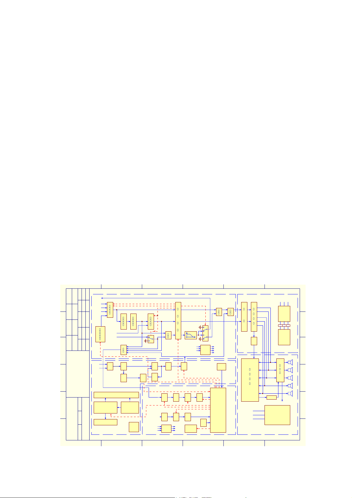
Ⅶ. The principle figure of entire device is as follows:
F
更 改 数 量 更改单号 签 名 日 期
设 计 审 核
标 准 化
21
批 准
3
AV210TÔ-Àí¿òͼ
4
广东步步高电子工业有限公司
第 张
5
共 张 版次:
6
F
BBK
E
SW-out
VCD(L/R)
DVD(L/R)
5.1CH(L/R)
Tuner(L/R)
MIC1
MIC2
A
输入选择
BB
L/R
跟随缓冲
合成解码
L/R
数字调谐器
5.1CH(C/SL/SR)
5.1CH(SW)
DO/CL/DI/CE
OK
音量
VFD显示
DISPLY ÖжÏ
驱动电路
按键阵列
面 控 板
S-C
混合
D-SW
C/SL/SR
MIC
前置
放大
放大 检测
电源
灯丝/负压/+5V
遥控
接收
E
КдИлС¡Фс
D
A
SEL
电
C/SL/SR
程控
放大
检入
放大
±6.8V
D
电源
混合
提升
子
音
量
SW SW
ST1/DA1/CK1
MIC
带通
滤波
双限
比较
+6.8V
AGND
-6.8V
通道选择
SEL
S-C
D-SW
电子
混响
混响
调节
P_KT
+12V
AGND
-12V
MUT1
静音
C
SW
L/R L/R
MUT1
C/SL/SRC/SL/SRS-C/S-SL/S-SR
低通
+12V
电源
AGND
-12V
±6.8V
+5V
P_KM
通道
采样
切换
P_SELECT
P_SEARCH
检测
复位
电路
EEPROM
24C02
C
信 号 板 功 放 板
混合
混合
MIC
SW
Êä³öÇл»
±¬ÅïÇý¶¯ºÍÏß·
+6.8V
AGND
-6.8V
+5V
½ÓÊÕÍ·
P_REM
P_CHARGE
CPU
CPU板
B
静
音
B
Vc+
AGND
Vc-
功
率
放
大
过载
检测
保
护
电
路
L
R
C
SL
SR
¼МµзЖчЗэ¶¯
电 源 板
A
+12V
AGND
前置
电源
Vs+ GND Vs-
中环
电源
继
电
器
SW¾²ÒôºÍ¼ÌµçÆ÷״̬¼ì²â
主功放电源
A
1
-12V
2
3
L
R
4
C
SL
SR
5
6
2
Page 3

更改:Amendment
数量: Quantity
更改单号:Amendment sheet No.
签名:Signature
日期:Date
设计:Designed by
审核:Examined and verified by
标准化:Standardization
AV210T 原理框图: AV210T principle figure
第 张: Page
共 张: Total pages
版次: Edition
广东步步高电子工业有限公司 BBK Electronics Corp., Ltd.
输入选择 Input selection
跟随缓冲 Follower buffer
合成解码 Cyber logic
通道选择 Channel selection
电子音量 Electronic volume
信号板 Signal panel
混合 Mixed
混合 Mixed
数字调谐器 Digital tuner
输入选择 Input selection
混合 Mixed
低通 Low pass
爆棚驱动和线路输出切换 Bass enhancer and circuit output switch
电源 Power supply
功放板 Amplification panel
静音 Mute
功率放大 Power amplification
前置电源 Front power
中环电源 Central surround power
过载检测 Overload detection
前置放大 Preamplification
放大 Amplification
检测 Detection
电子混响 Electronic echo
混响调节 Echo adjustment
提升 Promote
静音 Mute
接收头 Receiver
保护电路 Protection circuit
继电器 Delay
继电器驱动 Delay driver
3
Page 4

SW 静音和继电器状态检测 SW mute and delay-status detection
主功放电源 Main amplification power supply
电源板 Power board
VFD 显示 VFD display
驱动电路 Drive circuit
电源 Power supply
灯丝/负压/+5V: Filament/Positive voltage/+5V
按键阵列 Button matrix
遥控接收 Remote control receiver
面控板 Control panel
程控放大 Process control amplification
带通滤波 Band pass filter
通道切换 Channel switch
采样 Sampling
中断 Cut off
检入放大 Input amplification
双限比较 Double comparison
检测 Detection
复位电路 Reset circuit
电源 Power supply
CPU 板 CPU panel
Section 2 Power Circuit
It provides required working voltages to element circuits. AV210T (RU) adapts a
loop transformer of 133W. The central and surround channels of AV210T (RU) adopt
dedicated power amplifier IC, and its left and right surround channels and central
channels adopt power amplifiers LM4731 and LM1875. And two channels of LM4731
use independent positive power supply to assure super separation between two
surround channels. Compared with the predecessors, it adds ±22V power supply as
well as standby function. The main purpose is to enter into standby without output of
main power amplifier by using CPU software program to cut off the relay in standby
mode. See the power supply and circuit diagram as follows:
Ⅰ. The DC power supply of ±36V is obtained via the rectification and filtration of
two sets of AC 26.5V outputted from the transformer at first sublevel by four IN5404s
and two big electrolytic capacitors (6800uF, 50V), providing power to left and right
channels.
Ⅱ. The power supply of ±22V is obtained via the rectification and filtration of two
sets of AC 16V voltages outputted from the transformer at second sublevel by four
4
Page 5
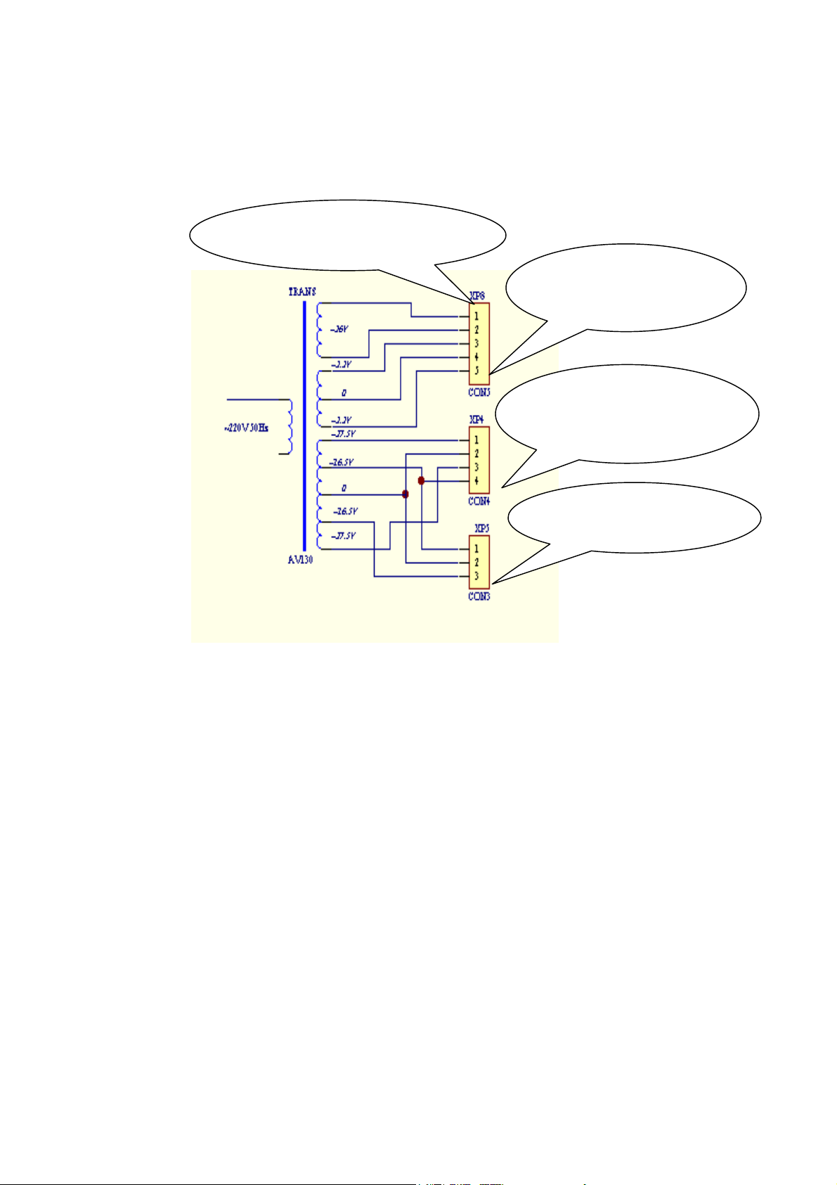
IN5404s and two electrolytic capacitors (4700uF, 25V), providing power to SL, SR, C
r
r
y
p
channels, and also to other IC and operational amplifiers after voltage stabilizing via
voltage stabilizing tubes L7812 and L7912;
Provide PT6311 with drive power
Provide display with
filament voltage voltage
Provide main powe
amplifier circuit with powe
suppl
Provide SL/SR/C with
ower supply
Section 3 Input, Cyber Logic, Volume Control Circuit
The cyber logic function of AV210T(RU)is realized by C, SR, SL and SW channel signals
obtained after processing signals extracted on L, R channel by using low pass filter and band
pass filter. This circuit uses several electronic analogue switches to fulfill switching between
different modes (See Figure II for signal flow).
I. Input selection and mode switching circuit
AV210T(RU)has two sets of analogue audio source input modes and a set of 5.1 input
interface. The switching between them is releazed by using electronic switch. Two types of
electronic switch IC are used in the circuit: CD4052 (2-channel 4-option electronic analogue
switch) and CD4053 (3-channel 2-option electronic analogue switch). Their truth tables are
as follows:
5
Page 6
CD4052 Truth
h
N
N
N
N
N
t
N
N
N
N
N
N
CD4053 Trut
X0 X1 X2 X3
0
A
B
1
0
0
XBY C
A
1
0
1
1
0
1
X0
X1 1
0
Y0
Y1
Z
Z0
0
Z1
1
In this circuit, there are another two important control signals, i.e. SEL and MUT1.
When SEL is of high level, the circuit is in external “5.1 channel” input mode; when SEL is
of low level, the circuit is in “cyber logic” mode; when MUT1 is of high level, “bass
enhancer” function will be enabled; when SEL and MUT1 are all of low level, the circuit is
in standard sound field processing mode. Here is a detailed analysis:
When pressing “input” button, PT6311 on the control panel will recognize the code and
send an execution request signal to CPU. Then the 32nd pin of CPU (N100) will return a data
signal to M62446. According to the “input” button status, the 1st, 2nd, 3rd, 4th pin of M62446
sends corresponding high, low levels, the combination of which will enable electronic switch
to circularly select between VCD→DVD→5.1CH→Radiohead. Now there are mainly two
statuses: two analogue input statuses (VCD, DVD) and 5.1CH input status. Their respective
signal flows are as follows:
1. 5.1 Input status: When A, B, SEL control lines of M62446 are of high level, L, R
channel signal of 5.1 input end is outputted from pin 3, 13 of N101 and sent to IC N106 for
functional adjustments of channel volume, sound field balance, etc.; meanwhile, the 4th pin of
N106 outputs a high level to pin 9, 10, 11 of electronic switch N102 (i.e. SEL control signal),
104B
VCD
5.1 inpu
L/R
channel
C/SR/SL
channel
5.1input
SW
6
N101
CD4052
input
selection
SL
SR
c
SW1
N102
CD4053
electronic
switch
104A
107B
N103
CD4053
electronic
switch
105B
SW
105A5.1 input
107A
to L/R
L
R
SW
C
SR
SL
15
M62446
electronic
13
volume
6
control
11
8
9
103B
SEARCH
106
108B
103A
100
CPU
(Fig. 2)
Page 7

and C, SR, SL signal on 5.1 input terminal is respectively sent from pin 14, 15, 4 output of
N410 to IC N106 for independent volume control. SW channel signal on 5.1 input terminal is
sent to pin 3 of IC N103, while pin 9 (SEL) is of high level, and SW signal is sent from pin 4
output to IC N106 for volume control. Now the six channel signals of 5.1 input terminal are
all sent to electronic volume control IC for independent volume control and then outputted
post pole circuit. The signal source of the device is in 5.1 channel input mode.
2. Two analog tuning, input modes: Press the “input” button on the panel to select
from two analogue input modes of VCD and DVD as signal source. The selection is also
realized via data signal sent from pin 32 of CPU N100 using pin 1, 2, 3, 4 of M62446 to send
two control levels of A, B, SEL and MET1 to pin 9, 10 of electronic switch N101 (pin 9, 10,
11 of N102 and N103). L, R channel signal is subject to volume, tone control and sound field
mode directly via M62446 from pin 3, 13 output. AV210T(RU)has three processing modes
for signals: hi-fi, cyber logic, standard sound field. Their respective signal flows are as
follows:
1) Standard sound field processing mode: L, R channel signals outputted from N101 are
directly added to IC N106 for electronic main volume control. Meanwhile, SW signal
obtained by amplifying a signal from L, R channel via N104 voltage followed by
N105A and N107A two-level low pass filtering is added to pin 6 of electronic volume
M62446 for electronic volume control. MUT1 is of low level; now the device is in 3channel output mode. When MUT1 is of high level, “bass enhancer” function is
enabled. Now the device is in 2-channel output mode.
2) Hi-fi processing mode: The signal flow is same as that of standard sound field mode, but
under the control of CPU, electronic volume control IC N106 closes other channels and
disables sound field processing and balance control. Therefore, SW signal has no output
and the device is in 2-channel output mode.
3) Cyber logic mode: L, R channel signal signals outputted from N101 are directly added to
IC N106 for electronic main volume control. Meanwhile, two ways of surround channel
signals are obtained by adding and subtracting using N105(4558)after amplifying two
ways of signals from L, R channel via N104, central channel signal is obtained through
N105A, and SW signal source is obtained through N107A inverse amplification, and is
inputted to pin 6 of M62446 (Note: SW signal of cyber logic is obtained through the
output terminal of M62446 and then through a 2nd order low-pass filter); Now pin 9, 10,
11 (SEL) is of low level and SW signal source is directly sent to pin 6 of M62446 for
electronic volume control. MUT1 is of low level, and now the device is in 2-channel
input and 6-channel output mode; when MUT1 is of high level, “bass enhancer”
function is enabled and now the device is in 2-channel input and 5-channel output mode.
The relations between switching between audio sources of input circuit and sound
processing modes are as follows.
7
Page 8

Only L/R channel output;
d
Press “input”
button for
circular
selection
Two
analog
input
modes
Hi-fi
mode
Standard
sound
field
mode
Cyber
logic
mode
sound field and EQ setting
are invalid
Only L/R/SW channel
output, music hall soun
field and EQ setting are
available
6CH output, theatre
sound field and EQ
settings are available
5.1CH
input
mode
6CH output, theatre
sound field and EQ
settings are available
II. Volume control, sound field processing and EQ control circuit
Channel signals are finally sent into N106 to fulfill independent volume control, EQ
control and different sound field mode processing, etc.
Sound field processing and EQ control circuit is mainly for the processing of L, R main
channel signals. As seen from the schematic diagram, L, R channel signals are sent to pin 13,
15 of N106. When the device is in hi-fi mode, CPU software program will control M62446
and mute other channels, and volume control is only available for L, R channel, and only pin
31, 32 has signal output, while the device is in 2-channel output mode; when the sound field
mode of the device is not in hi-fi mode, independent volume control of each channel and
sound field processing or balance control of L, R main channel are available. Finally, signals
of different channels will be outputted from pin 31, 32, 33, 34, 35, 36 of N106. SW channel
signal outputted from pin 36 will be sent into pin 1, 12 of N103 after passing an active low
pass filter. The level signal of MUT1 will decide whether outputting it to an active speaker
for amplification by SW output terminal or sending it to main channel to enable “bass
enhancer” function. Other channel signals will be sent into power amplifier circuit for post
power amplification. L, R channel signal will pass two-level mixed amplification (superpose
SW or karaoke signal onto L, R channel).
“Bass enhancer” function:
”Bass enhancer” function is to send subwoofer to left and right channels respectively so
as to enhance the bass effect on main channel. At this time subwoofer has no output and an
active subwoofer can be saved; but this will increase the power load on main channel,
placing a high requirement on post amplifier. Primarily comparing with standard sound field,
cyber logic, 5.1 input sound field mode. Its operating principle is as follows:
When the device is in any of the three modes and “bass enhancer” function is enabled,
CPU will send a data signal to IC M62446, pin 32 of which will send a high level signal to
8
Page 9

pin 10, 11 of N103, so that pin 14 of N103 will be grounded (signal outputted to SW is
closed), and SW signal will be outputted from pin 15 of N103 to the reverse phase of N109A,
N109B for mixed amplification with L, R channel, followed by post amplification in main
channel power amplifier circuit after N110 amplification. For the three modes of “bass
enhancer”, gradual volume increase is done by IC M62446.
III. Input signal detection, search and spectrum sampling circuit
1. Input signal detection, search circuit: After synthesizing and gating, input signals are
mixed by sample resistances R133, R134, R135, R136 and R195 connected to the output
terminals of N102 and N103 and then amplified at the inverted input terminal of N108A.
Then input signals are level amplified and clipped by N103A on CPU board, and then sent
into voltage comparator made up of N103B. The output terminal of N103B is connected to
pin 16 of CPU through a triode (switch tube). When the output terminal of N103B outputs a
high level, VD103 is in inverse cutoff state and the E pole of switch tube V101 is of high
level. Therefore, the switch tube is in conducing state. Then through voltage regulation by
VD101, an obtained high level of about +5V returns to CPU, indicating inputted signal is
detected; when the output terminal of N103B outputs a low level, VD103 is in positive
conducing state, and the E pole of switch tube V101 is of low level. Therefore, the switch
tube is in cutoff state. Through VD101, a low level returns to CPU, indicating there is no
signal input; when it is of low level, CPU stops search. See details below:
1) After startup, pin 32 outputs a data signal to M62446 under the control of CPU internal
program, and then M62446 sends high, low level to scan each input port of N101, N102,
N103. When none of these input ports has signal input, it will automatically stop in VCD
mode (display “connect to VCD”). When one input port has signal input, and this signal
is greater than about 15mV, AC signals will be present on channels of N101. This AC part,
after N104 amplification and amplification on N105A, N108B and N103A on CPU board
and level clipping, is compared with pin 1 of N103B and then a high, low level of power
supply is obtained. Now the voltage on reverse end of N103B is about 0.35V. When this
DC voltage exceeds 0.35V, the output terminal of N103B outputs high level close to
positive supply voltage, so via the switch tube V101 (S9014) and voltage regulator tube
VD101, a high level of +5v returns to pin 16 of CPU, indicating CPU has searched signal,
the CPU locks search level on this port with signal input via controlling IC M62446 and
enters into normal playback.
2) When “search” button on remote controller is pressed, optical signal received by remote
control receiver is converted into electric signal, and then pin 14 of CPU sends a high
level to put V102 into conducing state. Search is done in the same way as procedure 1).
3) At the same time, AV210T(RU) has “auto mute” function: When input signal is less than
about 1mV, CPU will put the device into “auto mute” mode; the signal control flowchart
is as follows: When CPU “finds” signal, pin 14 of CPU will immediately shift into low
level, so that V102 is in cutoff mode. After +12V is voltage divided by R113 (180K) and
R114 (100Ω), a voltage of about 1mV is obtained on the positive end of N103B.
Therefore, external signal, after sampling and amplification, is compared with this
voltage. If it is smaller than this voltage, CPU turns the device into “auto mute” mode; or
9
Page 10

when CPU has not found signal, the device will also be turned into “auto mute” mode by
comparing of voltage division between the reverse end and R1113, R114.
2. Spectrum sampling and amplification circuit: Signal channels have sample resistances
R133, R134, R135, R136 and R195 respectively. After signals are mixed by them and sent to
be amplified by N108B, spectrum analysis signal source (DISPLAY) is obtained and sent to
band pass filter circuit of CPU board.
Section 4 Overall Control Circuit
The overall control circuit of AV210T(RU) is divided into three parts, i.e. CPU circuit,
panel control and display drive circuit, spectrum analysis circuit.
I. CPU circuit
N100 (W78E58) is the overall CPU, being the processing and control center of the device
that outputs control commands to controlled circuits and fulfills control functions. It adopts
+5V power supply and pin 40 is the power supply pin. 12M crystal oscillator connected to
pin 18, 19 provides working clock frequency. Pin 9 is its reset pin. Upon startup, +5V is
added to the positive pole of C106 via R100. Since the charge of C106 is conduced via triode
V100 positively that forms an instant high level outputted to pin 9 of N100 which returns to
low level as the finish of charge and the reset ends. The form of this resetting circuit is to
delay high level reset and maintain low level. Refer other control commands to circuit
diagram. Here do not explain in details.
The startup picture, Chinese characters displayed during operation and other static
information are saved in the built-in static memory of CPU. N101 is a status register that
records working statuses upon shutdown and recalls these statuses upon the next startup,
avoiding readjustment by the user. User defined sound field mode is also saved in it and can
be recalled when required.
II. Panel control and display circuit
The panel control and display circuit of AV210T(RU)uses dedicated IC 101 (PT6311).
Its pin 10, 11, 12, 13 are externally connected to scan button matrix. After the overall control
command from the user is received, two-way outputs are available: one way is sent to the
display to show its working status and another way is transmitted to CPU via pin 5, 6, 8, 9 for
requesting the execution and fulfillment of corresponding control function.
N102 is a remote control receiver that transforms infrared remote control signal into
electric signal and then send it to pin 13 of CPU to fulfill remote control function.
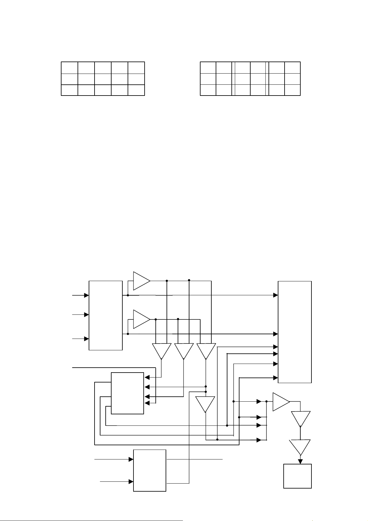
III. Spectrum analysis circuit (see flowchart diagram below):
10
Page 11

N
seven segment band pass
N
N
N
DISPLAY
+5V
N104
CD4051
auto spectrum
gain adjustment
V103
105C
+
3
.
}
CPU
+
-
102B
.
102A
V105
V104
35HZ
100HZ
300HZ
1KHZ
3KHZ
10KHZ
16KHZ
108
CD4051
frequency
point
gating
CPU pin 12
CPU pin 28
}
CPU
3
A/D conversion
Spectrum analysis circuit can be divided into three parts:
1. Automatic spectrum gain adjustment circuit: To avoid ultra low width spectrum display
when the input signal is too weak or full screen display when the input signal is too strong,
AV210T(RU), as its predecessors, provides automatic spectrum gain adjustment circuit,
using a single channel select-1-from-8 electronic analog switch N104 (CD4051), the truth
table of which is as follows.
Its working principle is, generally, to change the value of the reverse ground resistance of
operational amplifier N104 by switch selection so as to change the gain times of operational
amplifier. Let us see the specific working process of the whole circuit.
CD4051 Truth
X0 X1 X2 X3
1
0
A
0
B
C0
0
000
0
1
X4 X5 X6 X7
1
0
1
0
1
1
0 1
1
1
0
1
1
1
The abovementioned spectrum analysis signal source (DISPLAY) is sent into the
in-phase input terminal of operational amplifier N105C for amplification. The amplification
times is dependent on the value of the resistance connected to the reverse end via N104
electronic switch. When the input signal has a rather high amplitude, CPU will automatically
increase ground resistance value and reduce amplification times to reduce the gain; when the
input signal amplitude is rather smaller, CPU will automatically reduce the value of ground
resistance and increase amplification times.
2. Frequency point gating circuit: Signals amplified via N417B and coupled by C114 are
11
Page 12
sent into 7 band pass filters made up of operational amplifiers. By setting its feedback
N
capacitance its corresponding frequency band range can be determined. The frequency values
marked on their output points are the central frequency points of this frequency band. A
half-wave rectification circuit is connected to the output terminal of each band pass filter to
rectify amplified AC signal into DC voltage. This circuit is mainly for the realization of
frequency point sampling and can present the amplitude of each frequency point in a
complete sound signal through DC voltage. If low frequency prevails in sound signal, DC
voltage on 35HZ, 100HZ band pass filter will be higher. It is the same that DC voltage on
10K, 16K band pass filter will be higher if the high frequency prevails. The output terminal
of these seven band pass filters are connected to the seven input terminals of electronic
switch N108 (CD4051) and this electronic switch can realize rapid gating between frequency
points via control commands sent by CPU (refer to the above truth table). A series of voltage
values representing frequency point signal amplitudes will be outputted on the output
terminal of pin 3 of N108. (See the following fig.)
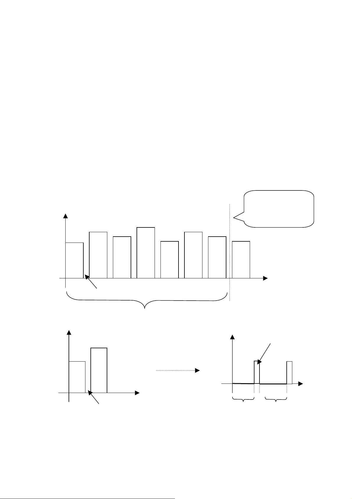
3. A, D conversion, display output circuit (discussed in two cases)
V
35HZ
100HZ
300HZ
1KHZ
3KHZ
10KHZ
16KHZ
35HZ
ote: The voltage
amplitudes in the
figure are not definite
T
Time interval of switching
V
Frequency point circular gating cycle
35HZ
100HZ
V
High level
discharging
Time interval of switching
T
(Fig 6)
35HZ
Charging time
100HZ
T
Charging time
1. When there is no signal input (i.e. no detect-in signal), CPU’s pin 28 will send a high level
to V104’s C pole to put it into conducing state. And since E pole and B pole of V103 are
provided with +5V power supply and a biasing circuit made up of VD115 and VD116,
12
Page 13

maintaining V103 in conducing state, so the circuit will not charge up C137, the positive end
r
of N102B is of low voltage and the reverse end of N102B obtains voltage division of R169
and R172, and so N102B will output a low level, i.e., triode V105 cuts off, and V105’s C
pole will send a high level to pin CPU’s pin 12, informing CPU no to conduct AD conversion
(CPU’s pin 6, 7, 8 does not act, maintaining at high level.)
2. When the device detects signal (i.e. when a DC voltage representing 35HZ signal
amplitude is present on the reverse end of N102B), CPU’s pin 28 will immediately be
converted into low level, and meanwhile, +5V provides V103 with conducing condition and
outputs high level from V103’s C pole and charges up C137, the positive end (the inphase
end of N102B) voltage of which will increase gradually. When the voltage on reverse end is
reached, the comparator inverts, and N102B output is close to the high level of positive
supply voltage. Once the comparator inverts, CPU will immediately terminates 35HZ level
gating and switch to the next frequency point 100HZ. During the interval of their switching,
an instant high level outputted from CPU’s pin 1 gates V104 and discharges the voltage
capacity on C137, allowing the in-phase end of N102B to resume 100HZ charging from 0
level. When 100HZ charging is complete, it will turn into the next charging and discharging
process for the next frequency point. Such processes will be circulated under CPU control.
The charging time from 0 level to the occurrence of output inversion represents the signal
amplitude of the current frequency point—the greater the amplitude is and the longer the
time is, the higher the amplitude displayed on the screen will be; the smaller the amplitude is
and the shorter the time is, the lower the amplitude displayed on the screen will be. As known
from the above circuit working process, a series of analog DC levels originally with specific
voltage values become a series of digital pulses only with two states of 0 and 1 presenting the
original information by its time duration. And so the conversion of analog/digital (A/D) is
done. Digital pulses outputted from the output terminal of N102B, inverted by V105, are sent
to pin 12 of the CPU, which process and output them to panel display IC N101 for dynamic
spectrum display on the display. Originally frequency points are displayed in order, but what
we see on the display is a working process with the whole spectrum displayed simultaneously
since the above-mentioned circulating process is so rapid.
Section 5 Microphone Circuit
Ⅰ. Microphone circuit can be divided into two parts: preprocessing and reverberation
processing. The flow diagram is as follows:
OK
volume
Preamplifie
Amplifier
Detect
13
Electro
nic
echo
Echo
reverbe
adjust
ration
Promote
Mute
Page 14

Ⅱ. Preprocessing circuit: to fulfill volume control, amplification and modifying.
Two-way MIC signals inputted by two-way microphone jacks, after preamplification,
are divided into two ways, one is sent to the reverse end of N906 for inverse amplification
followed by rectification and filtration via VD103, R208, C206 producing a high level, so
that V103 is turned on, and V103’s C pole returns a low level to CPU, indicating that MIC
signal is found; the other, via double rotary potentiometer, after being amplified by multi
small signals, then mixed and amplified with high frequency signals obtained via a high
frequency boost network, and then send to reverberation and delay IC PT2399, the IC of
which fulfills the reverberation and delay of karaoke.
There are two independent ways for the volume control of this device which is
controlled by the rotary potentiometer on panel. The basic principle is that to achieve the
purpose of increase or decrease the signal via increasing or decreasing the resistance value of
the signal channel.
Ⅲ. Echo processing: After being coupled by C213 and R224, signals are inputted into pin
16 of echo processing IC N113 (PT2399), in the inside of which signals are subject to low
pass amplification and digital delay processing, and then outputted from pin 14. Pin 6 is
externally connected to echo delay adjustment resistance. Delay and echo adjustment of this
device are directly controlled by potentiometer. The time of delay can be changed by
adjusting the outer delay resistance of pin 6. The feedback resistance of echo feedback loop
can be changed by adjusting PR904 potentiometer thus to change the feedback coefficient as
to adjust the echo. And besides, karaoke is provided with auto mute function against
microphone insertion impact sound. This control process is as follows (in two states):
1. When the device is reset, CPU’s pin 25 will immediately outputs a high level to
conduce V100 via R193, so as to conduce V101, making short circuit to earthing of
MIC signals, so as to mute karaoke noise signals;
2. When inserting a microphone and signals are detected by CPU’s pin 5, CPU’s pin 25
will returns a low level. Due to charging and discharging of C169, the cutoff of V100
and V101 requires a waiting time, so the impact sound and mechanical noise can be
removed effectively.
14
Page 15

Section 6 Power Amplifier and Protection Circuit
r
r
k
y
The description and block diagram of the working principle of main power amplifier
circuit are as follows:
AC negative feedbac
R121, R108, C105
L In
V101
V115
Mute
Differential
amplifier
stage
Mirror image constant
current source V104,
V107, VD102, VD103
Voltage
amplifier
stage
V105
I. L, R channel power amplifier circuit: The L, R main power amplifier circuit of AV210T
(RU) adopts discrete components. Its circuitry principle is as follows (taking L channel as
example).
When being outputted by electronic volume control circuit, L channel signal is sent to
power amplifier stage. Mute circuit is provided on the input terminal: When the mute button
on remote control is pressed, a “mute” signal is obtained after photovoltaic conversion by
remote control receiver and returned to CPU, so that CPU’s pin 35, 36 send a high level
“mute” command, allowing positive biased conduction of V115 (main channel) and V130
(central channel), and V101 is successively conduced, fulfilling mute control.
L channel signal, after being coupled by R103 and C101, is sent to the differential
amplifier circuit with double ended input and single ended output consisting of B pole of
differential amplifier stage, V102 and V103. Audio signal is outputted from C pole of V102
to B pole of voltage amplifier stage V105, and outputted to compound power amplifier stage
after voltage amplification. V104, V107, VD102 and VD103 constitute mirror image
constant current source circuit. VD102 and VD103 provide V104 and V106 with constant
base current. The emitter resistance of V104 determines the working current of differential
amplifier stage and the emitter resistance of V107 determines the working current of voltage
amplifier stage. V108, V109 and V112 constitute the upper tube (NPN) of the composite
power amplifier. V108 and V109 are connected in parallel, acting as a triode (to increase
output power), and composite with V112 to constitute NPN type multiunit tube (to increase
amplification times). V110, V111 and V113 constitute the lower tube (PNP) of the composite
power amplifier. Its circuit structure is same as that of the upper tube but its type after
composting is PNP. Temperature compensation tube V106 plays two roles in the circuit: First
Composite powe
amplifier (NPN)
V108, V109, V112
Temperature
.
compensation stage
V121
Composite powe
amplifier (PNP)
V123, V124,
V127
.
Rela
Sound
15
Page 16

it is the base bias of upper and lower geminate transistors, and its working status determines
the static working current of the composite power amplifier, that is to say, we can set the
static working point of the composite power amplifier stage by adjusting the conduction of
V106 and the usual way is to change the base resistance of V107; it can also automatically
adjust the working status of composite power amplifier stage upon temperature rise. The
adjustment process is as follows:
Total current of output stage = working current + leakage current
When the temperature rises, the increase of leakage current causes drift of static working
points (disadvantageous)
Meanwhile, the leakage current of V106 increases and Uce decreases,
reducing the bias current, changing working status and working
current of post pole. The total current is controlled within a certain
range.
Voltage negative feedback is introduced into the power amplification circuit of AV210T
(RU)and consists of R121, R109 and C105, the parameters of which determine the major
closed-loop gain times of the whole power amplifier. The formula is: gain times = 1 + R121
÷R109. AV210T(RU) uses direct output and R111 and C116 connected to the output
terminal constitute Zobel network, which can prevent high frequency self-excitation caused
by AC inductive reactance of loudspeaker voice coil.
II. C, SR, SL power amplifier circuit: Compared with its predecessors, these three channels
of AV210T(RU) use dedicated power amplifiers LM4731 and IC LM1875. For LM4731, it
has totally 15 pins. Pins 2, 4, 15 are its positive and negative power supply pins, and pins 7, 8,
12, 13 are its in-phase and reverse input terminals. Meanwhile, it uses independent positive
power supply for two channels. The rated power of each channel of this power IC can reach
25W. The high level automatically “mutes” upon startup. Pins 7, 8, 12, 13 are its signal input
terminals and pins 3, 1 are their signal output terminals; for LM1875, it has totally 5 pins,
being a high-performance single-channel power amplifier IC. The applied circuit is very
simple and has a 15W power output in rated status. Pin 5 and pin 3 are positive and negative
power supply pins. ±22V power supply is used in this device. Pin 1 is signal input terminal,
pin 2 is feedback input terminal and pin 4 is output terminal.
III. Protection circuit: The way of protection for L, R channel is to disconnect relay Y100
and to disable output. For the protection of C, SR, SL channel, is to disconnect relay Y402 to
disable output. Their control terminals are connected to disable outputs of five channels upon
startup. AV210T(RU)has the following ways of protection:
1. Startup delay closing protection circuit: Since that the circuit is unstable upon startup
and the impact current produced greatly harms the sound box and power amplifier circuit, so
delay closing protection circuit is provided. Upon startup, +22V charges up C115 via R108,
and the positive voltage of C115 rises gradually. When it exceeds 5.1V, VD411 is inversely
struck through, and its positive pole outputs high level to add to the base electrodes of the
compound tube made up of V105 and V104. Now the compound tube is conduced, relay
Y100 closes and the device has normal output. The startup delay closing time depends on the
charging and discharging time constant. Its working process is as follows: +22V charges up
16
Page 17

C115 via R108 and strikes through down VD111 inversely, so as to conduce V105, V104
n
V
d
h
n
positively and finally close relay Y100. Left, right and central channels conduct startup
impact protection in the following way: When the system is reset, CPU’s pin 33 outputs a
high level, which goes through R164 and pin 9, 14 of LM4731 to make LM4731 to output
mute. After the successful delayed startup of device and normal closing of the delay, the level
of CPU’s pin 33 is reduced and shifted to low level, so that LM4731 begins to enter normal
working status and SL, SR channel outputs normally.
2. Middle point overvoltage protection: An overvoltage sampling resistance is connected to
the output terminal of each channel. L channel is R116. When the output middle point of a
channel has a DC voltage greater than +3.5V or lower than -3.5V, V101 or V102 is conduced,
reducing their C pole voltage. V103 is then conduced and finally the relay is disconnected to
protect circuit startup.
Channels are
connected with
overvoltage
sample
resistances
L CH
is
R116
More tha
+3.5
Less than
+3.5V
V101
conduce
V102
conducted
C pole
voltage
decrease
V103
conduced
Relay
disconnection
protection is
activated
3. Overcurrent and short circuit protection: An overcurrent sampling triode is connected
in parallel on each of the output load resistances of L, R channels. The sampling tube of L
channel is V114, the load resistances are R126 and R127. Other three channels are provided
with overcurrent protection in the power amplifier IC. When one of L, R channels is subject
to overcurrent failure, the voltage drop produced on R126 and R127 will increase rapidly.
Once the voltage drop produced on R129 exceeds 0.7V, V426 will be conduced. V103 is then
conduced and finally the relay is disconnected to protect circuit startup.
Channels are
connected wit
overcurrent
sample triodes
L CH is
V114
Upon
overcurrent,
the voltage
drop o
R126/R127
increases
V114
conduced
C pole
voltage
V103
conduced
disconnection
protection is
Relay
activated
17
Page 18

Section 7 Tuning Function
This device has the function of tuning which provides users a good functional option. It
directly controls radio head and receives audio frequency signal mainly via CPU and then
outputs after amplified via power amplifier. The clock and data line of radio head are shared
with LM62446 and the other two control lines are connected to CPU directly. L, R signal
processed by radio head can be sent to N101 IC CD4052 directly to input the selected
channel.
Fault analysis:
1. Auto mute with big signal:
Firstly, it can be thought as the problem of the circuit of auto mute, so to exam whether
there is short circuit with R113 on CPU panel. Since the signal can be automatically
inputted after its startup, the circuit of V102, R112 and R114 is good by primary
predication. But there is auto mute with big signal, so use multimeter to measure. If the
resistance of R113 is normal without short circuit, start the device again and find that
though CPU detected the signal, pin 14 of CPU is still in high level (theoretically, pin 14
of CPU will maintain low level after detecting signal), thus it will directly make the
voltage of reverse end of N103B increase as well as its mute valve value. This will cause
the above ill phenomenon but can be removed by changing CPU.
2. No screen display after power-on:
If the initial fuse of transformer is burned after startup and the fuse is also burned by
changing a new fuse and restarting the device, use multimeter to measure the primary of
transformer, the impedance of secondary coil of transformer is only 6.4 Ω, but the
primary impedance of transformer shall be about 12 Ω theoretically. So, it can be
concluded that there is short circuit with transformer primary. The problem can be
removed by changing a transformer.
3. No frequency spectrum when changing the songs:
The frequency spectrum display is normal when connecting with the signal after adding
sine wave signal and starting up. But there is low even no frequency spectrum when
pulling out and inserting again (adding the same signal source, the frequency amplitude is
the same). It indicates that there is no problem with the diversion of circuit of frequency
spectrum A, D if the device can be started and input signal normally and has the normal
frequency spectrum at the first time. Use multimeter to measure pin 28 of CPU, this
terminal is high level and it can be charged normally by cutting off R175 and C137 thus it
can be concluded that there is no problem with recharging circuit. Gradually increase
inputted signal and respectively test the level of pin 9, 10, 11 of N104, there is no
abnormity with frequency spectrum. Gradually decrease inputted signal and respectively
test the level of pin 9, 10, 11 of N104, find that if the level of pin 9, 10, 11 of N104 is all
high level, there will be low even no frequency spectrum. Exam the paste resistance of
R122 and find there is an omission of paste resistance. The ill phenomenon will be
removed by pasting 1.5K resistance.
18
 Loading...