

Page 1

Documentation
EVA4201/4301 – User Guide
Evaluation Board for
80W
Power Factor Corrected (PFC) Supply
Featured Products: PE4201/PE4301
Page 2

ISO 9001 / ISO 14001 01/06/2016 © Productivity Engineering GmbH
Page 2 of 22
EVA4204/4301
User Guide
Evaluation Board for 80W PFC Supply
Table of Contents
1.
Revision History ....................................................................................................................... 2
2.
Safety Instructions .................................................................................................................... 3
3.
Introduction .............................................................................................................................. 3
3.1
Features ................................................................................................................................... 3
3.2
IC`s General Description .......................................................................................................... 3
4
How to design an application ................................................................................................... 4
4.1
Given board specification ......................................................................................................... 4
4.2
Calculating the Current ............................................................................................................ 4
4.3
Inductor .................................................................................................................................... 6
4.4
Current Sense Resistor ............................................................................................................ 7
4.5
Error Amplifier Compensations .............................................................................................. 10
4.6
Self Biasing ............................................................................................................................. 11
4.7
EMI and Driver SlewRate ....................................................................................................... 12
4.8
Start-Up Bypass Rectifier ....................................................................................................... 12
5
Description ............................................................................................................................. 13
5.1
Evaluation Board Specifications ............................................................................................. 14
5.2
Wire bridges ........................................................................................................................... 14
5.3
Schematic .............................................................................................................................. 15
5.4
Component Placement........................................................................................................... 16
5.5
Board Picture and Layout ...................................................................................................... 17
5.6
Bill of Material ......................................................................................................................... 18
6
Operating ............................................................................................................................... 19
6.1
Caution ................................................................................................................................... 19
6.2
Load ....................................................................................................................................... 19
6.3
AC-Input ................................................................................................................................. 19
6.4
Power-up Sequence ............................................................................................................... 19
7.
List of Abbreviations ............................................................................................................... 20
8.
Notes ...................................................................................................................................... 21
9.
Contact Addresses ................................................................................................................. 22
1. Revision History
Version Date Changes Page
Initial Version V1.0 12/2008
V1.1 04/2013 Formula (2) 4
Page 3

ISO 9001 / ISO 14001 01/06/2016 © Productivity Engineering GmbH
Page 3 of 22
EVA4204/4301
User Guide
Evaluation Board for 80W PFC Supply
2. Safety Instructions
Please take caution - the board operates at 405V DC and is directly plugged into the power
network. Operating this Board requires an isolated transformer!
The EVA4201/4301 was designed to help understand and evaluate the features of two Power Factor
Correction IC`s. Used external devices are standard components chosen for safe operation and do not
represent a completely fine-tuned OEM application. The BOM (bill of material) for a final application may
look slightly different.
The board can also be used with PEs high precision PFC ICs, the PE4202 and the PE4302.
3. Introduction
3.1 Features
The board is designed to support applications of our two PFC-IC’s PE4201 and PE4301
PE4201 PE4301
- Low Total Harmonic Distortion (THD) - Wide Range Input
- Low StartUp Current (<5µA) - Low Total Harmonic Distortion (THD)
- Low Operating Current (<450µA) - Low Operating Current (<550µA)
- Disable Function (<170µA) - Disable Function (<100µA)
- Under-Voltage Lockout with >8V Hysteresis - Under-Voltage Lockout with >8V Hysteresis
- Over voltage and Over current protection with - Over voltage protection, Peak current
separate Reference protection and Open loop protection with
- Reduced operating Frequency at low Output separate Reference
Power - low Peak current protection threshold
- High Efficiency at high and low Output Power - Operating Frequency between 40 kHz and
- Internal Clamping Resistor at G 250 kHz dependent upon load
- fast Driver turn ‘off’ - High Efficiency at high and low Output Power
- very fast Driver ‘off’ at over current sense - Internal Clamping Resistor at Driver
- Driver load up to 5nF - Soft start
- fast Driver Switch ‘off’
Application with PE4201/PE4301
• Active power factor correction
• Switch mode power supplies
3.2 IC`s General Description
The PE4201 and PE4301 are wide input range controller ICs for active power factor correction
converters. Both ICs provide many protection functions, such over voltage protection, open loop
protection, supply under voltage lockout, output under voltage protection and peak current limit
protection. These protection functions are working with separate reference.
The PE4201 operates in the CRM with voltage mode PWM control and in DCM under light load
condition. The maximum switching frequency is clamped with an internal delay circuit. Compensations
for voltage loop are external.
The PE4301 IC operates in the CCM with average current control. The switching frequency depends upon
load. At high output load the frequency is low and with low load the frequency is high. The Compensation
for voltage loop and soft start is external.
For more information refer to the datasheets.
Page 4

ISO 9001 / ISO 14001 01/06/2016 © Productivity Engineering GmbH
Page 4 of 22
EVA4204/4301
User Guide
Evaluation Board for 80W PFC Supply
4 How to design an application
4.1 Given board specification
PE4201/PE4301
The board setup in the original state has the following specification parameters. The following chapters
show, what has to be changed to design an active PFC supply towards different parameters. Please
take caution when calculating. Wrong device parameter calculation can damage the Evaluation board or
other devices.
AC Line Input voltage 85 VAC ... 265 VAC
AC Line Frequency 47 ... 63Hz
Switching Frequency 40 ... 250 kHz
Output voltage 340 -405V DC (adjustable)
Output Load max 80W
Over Voltage Threshold 416V DC
4.2 Calculating the Current
PE4201
The input power:
86,96W=
92%
80W
=
η
out
P
=
in
P (1)
The input current:
A0,52=
110V
0,66*86,96W
=
AC
V
in
P
=
ACin_LL
I
D∗
(2)
A=
265V
86,96W
=
AC
V
in
P
=
ACin_HL
I
0,33
(3)
D… Duty Cycle at 110V
The peak current:
A=0,52A22=
ACin_LL
I22=
pk_LL
I
1,48
∗∗∗∗
(4)
A0,93=A33,022=
ACin_HL
I22=
pk_HL
I ∗∗∗∗
(5)
This peak current affects the component selection on the current sense resistor, Power-MOSFET, diode
and inductor.
Page 5

ISO 9001 / ISO 14001 01/06/2016 © Productivity Engineering GmbH
Page 5 of 22
EVA4204/4301
User Guide
Evaluation Board for 80W PFC Supply
0,11A0,40A20,220,2
ACin_LLLL
==I=∆I ∗∗∗∗
0,093A0,33A20,220,2
ACin_HLHL
==I=∆I ∗∗∗∗
,61A0
2
0,22
A40,02
2
2
LL
ACin_LLpk_LL
=+=
∆I
+I=I ∗∗
,51A0
2
0,22
A33,02
2
2
LL
ACin_HLpk_HL
=+=
∆I
+I=I ∗∗
PE4301
The input power:
86,96W
92%
80W
out
in
==
η
P
=P
(6)
The input current:
0,40A
110V
86,96W
AC
in
ACin_LL
==
V
P
=I
(7)
0,33A
265V
86,96W
AC
in
ACin_HL
==
V
P
=I
(8)
The ripple current ∆I is set to 20%
(9)
(10)
The peak current:
(11)
(12)
This peak current affects the component selection on the current sense resistor, MOSFET,
diode and inductor.
Page 6

ISO 9001 / ISO 14001 01/06/2016 © Productivity Engineering GmbH
Page 6 of 22
EVA4204/4301
User Guide
Evaluation Board for 80W PFC Supply
out
inout
V
VV=D−
0,615V
405
110V2405V
LL
==D
∗−
0,074V
405
265V2405V
HL
==D
∗−
4.3 Inductor
PE4201
For CRM operation, the maximum 'on' time and the maximum 'off' time control the lowest frequency.
The minimum CRM inductance L
(CRM)
at low and high line input voltage can be calculated as follows:
f
1
pk
I
in
V
out
V
in
V
out
V
=
(CRM)
L ∗∗
−
(13)
µH=
40kHz
1
1,48A
V2
405V
V2405V
=
(CRM)
L
1623
110110
∗
∗
∗
∗−
(14)
µH=
40kHz
1
0,93A
265V2
405V
265V2405V
=
(CRM)
L
754
∗
∗
∗
∗−
(15)
For high line voltage and high output power the inductor has to have a nominal inductance of 400µH.
The switching frequency at low line voltage can be calculated according to equation (16):
(CRM)
L
1
pk
I
in
V
out
V
in
V
out
V
=f ∗∗
−
(16)
39,9kHz=
1623µH
1
1,48A
110V2
405V
110V2405V
=f ∗
∗
∗
∗−
(17)
PE4301
For CCM operation, the maximum 'on' time and the maximum 'off' time control are the lowest
frequencies. The minimum CCM inductance L
(CCM)
at low and high line input voltage can be calculated
as follows:
Duty Cycle
(18)
(19)
(20)
CCM Inductor
Page 7

ISO 9001 / ISO 14001 01/06/2016 © Productivity Engineering GmbH
Page 7 of 22
EVA4204/4301
User Guide
Evaluation Board for 80W PFC Supply
∆If
DV
=L
∗
∗∗
in
CCM
2
(21)
µH21425
A11,040kHz
0,615110V2
CCM_LL
==L
∗
∗∗
(22)
µH7536
0,093A40kHz
0,074265V2
CCM_HL
==L
∗
∗∗
(23)
For high line voltage and high output power the inductor set to 8000µH.
The switching frequency at low line voltage obtains as:
∆IL
DV
=f
∗
∗∗
CCM
in
2
(24)
kHz6,109
A11,08000µH
0,62110V2
==f
∗
∗∗
(25)
4.4 Current Sense Resistor
PE4201
The current sense resistor provides the threshold voltage for the over-current protection function. The
maximum inductor peak current is set to 1,48 A.
0,15
Ω
=
1,48A
0,22V
=
OCP
I
SHPCP
V
=
s
R
(26)
R
sense
=0,15 Ω
PE4301
1,55
Ω
=
0,61A
0,95V
=
OCP
I
CSPCP
V
=
s
R
(27)
R
sense
=1,55 Ω
For higher/lower output power the resistor RS has to be reduced/increased and the inductor has to be
re-calculated.
Page 8

ISO 9001 / ISO 14001 01/06/2016 © Productivity Engineering GmbH
Page 8 of 22
EVA4204/4301
User Guide
Evaluation Board for 80W PFC Supply
2.5 Output Bypass Capacitor
PE4201/PE4301
The bypass capacitor on the output of the circuit has to be able to suppress the ripple of the switching
frequency and the residues of the full-wave rectified input frequency (2 * fin).
f
1
out
∆V
1
out
V
out
P
=
out
C ∗∗
(28)
It is recommended to use 4 * fin to suppress the sine wave residues of the input voltage for calculation.
The ripple shall be assumed to be at 5% of the output voltage.
at 40W :
34,2µF=
50Hz4
1
405V0.05
1
405V
40W2
=
out
C
∗
∗
∗
∗
∗
(29)
at 80W :
68,7µF=
50Hz4
1
405V0.05
1
405V
80W2
=
out
C
∗
∗
∗
∗
∗
(30)
A capacitor with at least 47µF (C13) should be used. It has to withstand the maximum output voltage.
The equivalent series resistance (ESR) of the capacitor shall not build up a voltage higher than half the
ripple amplitude (2,5% of V
out-max
) at peak-current.
16Ω=
0,61A
405V0,025
=
peak
I
out
∆
V
=
C
R
∗
(31)
To reduce the ESR it is recommend to place a capacitor with small ESR in parallel to the high
capacitance device. For 2% ripple at minimum switching frequencies the parallel capacitance can be
calculated according to equation (23):
0,61µF=
40kHz
1
405V0.02
1
405V
80W
=
out2
C ∗
∗
∗
(32)
The capacitor on the board is C12=100n/400V.
Page 9
ISO 9001 / ISO 14001 01/06/2016 © Productivity Engineering GmbH
Page 9 of 22
EVA4204/4301
User Guide
Evaluation Board for 80W PFC Supply
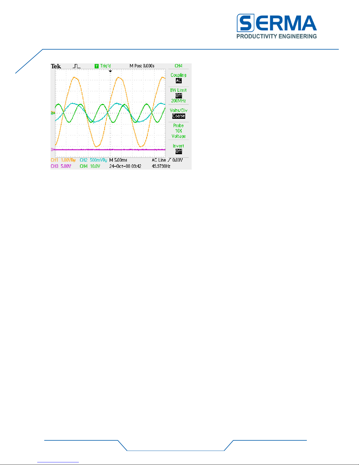
The figure shows the input voltage (230V~) in orange color, the current (I
out
=0.20A) in blue color and
the ripple of the output voltage in green color (only AC, C13=47µ, C6=0.1µ). The ripple is lower than
20V peak-to-peak (<5%).
Page 10
ISO 9001 / ISO 14001 01/06/2016 © Productivity Engineering GmbH
Page 10 of 22
EVA4204/4301
User Guide
Evaluation Board for 80W PFC Supply
Input Filter
PE4201/PE4301
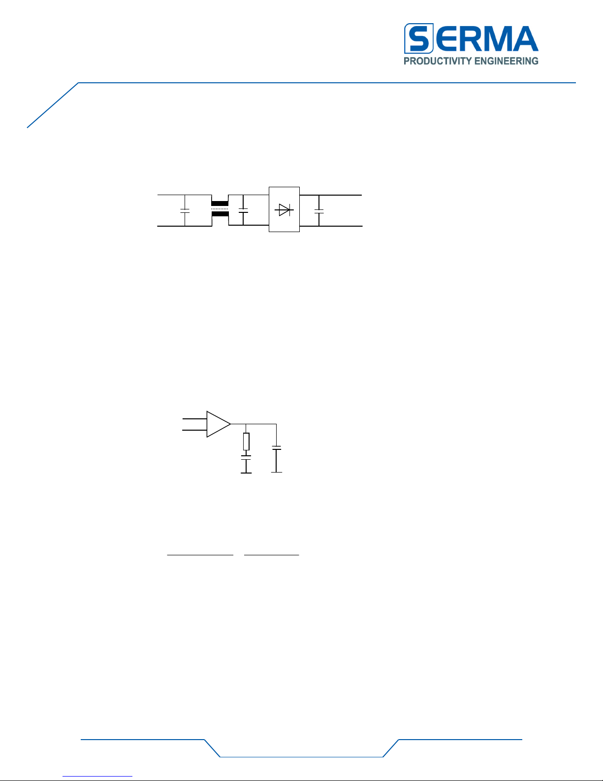
A high-frequency has to be applied in the primary AC input to reduce reflections from and to the power
grid.
Figure 1: Input Filter
The capacitor CHF following the bridge rectifier provides the peak current and reduces the voltage ripple.
This is typical for a 330nF or for a 470nF capacitor. A high capacitance here will decrease the power
factor (C1).
The L-C filter before the bridge rectifier has to suppress the switching frequency by about 20dB. The
cut-off frequency shall be below 10kHz.
4.5 Error Amplifier Compensations
PE4201/PE4301
The output of the integrated error amplifier has to be filtered by means of an RC filter for frequency
compensation.
Figure 2: Error Amplifier Compensation
At the same time the capacitor CSP ensures a soft start function. Capacitance can be calculated
according to equation (33). The soft start time is set up at 30ms.
237nF=
2,53V
20µA30ms
=
RREF
V
VCOmax
i
ss
t
=
z
C
∗
∗
(33)
C8=220nF shall be chosen here.
The frequency response should have a second pole slightly above twice the power grid frequency.
This is set up by RSP and CZ.
C
HF
C
EMI
2
C
EMI
1
L
EMI
AC
Lin
V
IN
VCO
IN
RRE
R
SP
C
Z
C
SP
Page 11

ISO 9001 / ISO 14001 01/06/2016 © Productivity Engineering GmbH
Page 11 of 22
EVA4204/4301
User Guide
Evaluation Board for 80W PFC Supply
6,028k=
220nF100Hz2
π
1
=
z
C
z
f2
π
1
=
SP
R
∗∗∗∗
(34)
R4=5,6kOhm shall be chosen here.
The frequency of the second pole shall be at about 1/7 of the switching frequency. This defines the
capacitance of CSP.
4,6nF=
6k5,7kHz2
π
1
=
SP
R
z
f2
π
1
=
SP
C
∗∗∗∗
(35)
C9=4,7nF shall be chosen here.
4.6 Self Biasing
PE4201/PE4301
Power supply of the PE4201/PE4301 during start up is provided through a high resistance resistor from
the power grid input voltage. The maximum resistance has to be calculated resulting from the minimum
input voltage and the required supply voltage of the PE4301 as well as the minimum required start up
current.
20Meg
Ω
=
5µA
20V85V2
=
ST
I
ST
V
in
V2
=
STUP
R
−∗
−∗
(36)
To reduce start up time and account for leakage currents in the external diode the resistor is chosen to
be 4MOhm. This is an experimental trade-off. Make sure the chosen resistor type has the proper power
dissipation. Also, relatively high voltage over the resistor is to be accounted for (245V). It is
recommended to use two 2MOhm resistors is series.
The capacitor on VDD has to provide power until the switching of the power-MOSFET has started and
power will be provided from the help winding on the transformer. That can only happen after start-up
and when the input voltage is at maximum level. At 50Hz this time t
VDD
is about 10ms.
Current consumption calculates from the IC supply current and the loss in the power-MOSFET when
switching.
Power consumption of the IC is <450µA. Power-MOSFET switching consumption consists of an ohmic
part (resistor on ‘G’) and the dynamical part in the MOSFET. This is a charge changing process at the
gate capacitance in the device.
Switching frequency will not be constant over an input frequency period. It can be assumed to be 150
kHz on average. Also the duty cycle factor will not be constant. For simplicity it can be assumed to be
50%.
A simplified but sufficient equation to calculate the dynamic and ohmic portion is given in equation (37)
and (38) respectively.
Page 12
ISO 9001 / ISO 14001 01/06/2016 © Productivity Engineering GmbH
Page 12 of 22
EVA4204/4301
User Guide
Evaluation Board for 80W PFC Supply
1,275mA=8,5V150kHz1nF=
Gmax
Uf
G
C=
Gdyn
I ∗∗∗∗
(37)
0,2125mA=0,5
20k
Ω
8,5V
=T
G
R
Gmax
U
=
Gohm
I ∗∗
(38)
Total current consumption calculates according to equation (39).
1,9375mA=0,2125mA+1,275mA+0,45mA=
Gohm
I+
Gdyn
I+
stat
I=
VDD
I
(39)
From that the capacitance of C
VVD
can be calculated:
1,38µF=
8V22V
10ms1,94mA
=
LO
V
ST
V
VDD
t
VDD
I
=
VDD
C
−
∗
−
∗
(40)
The help winding on the transformer has to provide between 20 ... 25V DC.
The Transformation Ration (TR) can be calculated according to equation (41):
18,4=
22V
405V
=
VDD
V
out
V
=TR
(41)
4.7 EMI and Driver SlewRate
PE4201/PE4301
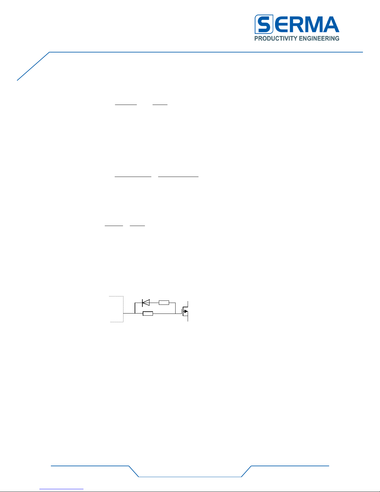
The driver slew rate can be influenced a network according to figure 3.
Figure 3: Network for Driver Slew Rate
R
tFALL
determines the Slew Rate of the falling edge (in practice 4.7 to 6.8Ω). The diode should be a fast
recovery Si-diode (MMSD914T1G).
R
tRISE
determines the Slew Rate of the rising edge (to optimize to gate capacity of the used FET, 18 to
56 Ω). Caution has to be taken to meet EMI regulations.
4.8 Start-Up Bypass Rectifier
PE4201/PE4301
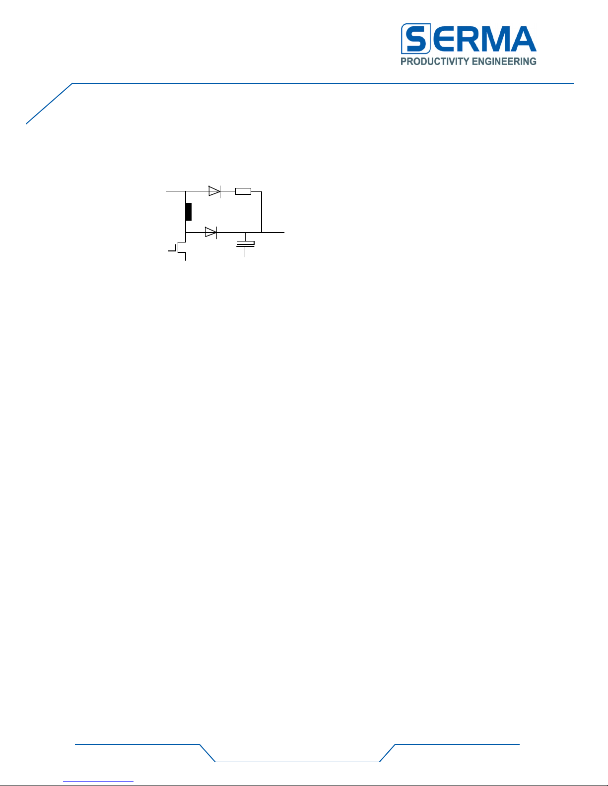
A diode (D
BYPASS
) in parallel to the coil and the boost diode (D
BOOST
) reduces the current through the coil
during start-up. It also pre-charges the bypass capacitor on the output to the peak input voltage.
This reduces over voltage peaks and currents in the coil and so improves EMI parameters. It also
protects the power-MOSFET from over voltage damage. To reduce the current through the diode a
series resistor shall be used.
G
R
tFALL
R
tRISE
Page 13
ISO 9001 / ISO 14001 01/06/2016 © Productivity Engineering GmbH
Page 13 of 22
EVA4204/4301
User Guide
Evaluation Board for 80W PFC Supply
In the range up to 80W, there is no need to use a bypass diode; the current depends on C
out
in addition
with possible start current on the load. In case of C
out=
47µF there is a max. current about 9A in a time
window of 4ms. The rectifier, inductors and boost- diode (R
sense
– PE4301) can handle it for such a
short time.
Figure 4: Bypass Rectifier
5 Description
The EVA4301-80 was designed to help understand and evaluate the features of the PE4201/PE4301
Power Factor Correction IC. Used external devices are standard components chosen for safe operation
and do not represent a completely fine-tuned OEM application. The BOM (bill of material) for a final
application may look slightly different.
The PE4201 is a wide input range controller IC for active power factor correction converters in CRMode
with voltage mode PWM control.
The PE4301 is a wide input range controller IC for active power factor correction converters in CCMode
with voltage mode frequency and PWM control.
Please take caution since the board operates at 405V DC.
V
IN
V
OUT
D
BYPAS
D
BOOST
Page 14
ISO 9001 / ISO 14001 01/06/2016 © Productivity Engineering GmbH
Page 14 of 22
EVA4204/4301
User Guide
Evaluation Board for 80W PFC Supply
5.1 Evaluation Board Specifications
AC Line Input voltage ...................................... 85 Vac - 265 VAC
AC Line Frequency .......................................... 47 – 65 Hz
Switching Frequency in the middle .................. 40 – 170 kHz
Output voltage .................................................. 340- 405V DC
Output Load ..................................................... max. 80W
Over Voltage Threshold ................................... 416V DC
Efficiency (@230V / 80W) ................................ 92%
Power Factor (@110V / 80W) .......................... 0.965
Power Factor (@230V / 80W) .......................... 0.990 (PE4301),
......................................................................... 0.988 (PE4201)
Operating Ambient Temp Range ...................... 0 – +40 °C
5.2 Wire bridges
The board has been designed to provide evaluation support for the PE4301 as well as the PE4201 PFC
ICs. For that reason the following wire bridges and components will have to be set properly.
PE4201 PE4301
JP1 2_3 1_2
JP2 1_3 1_2
R2*, R11*, C12* on Board open
R7**, C11**, R23** Open on Board
R
Sense
4x1.0Ώ/0.1W 3x4.7Ώ/0.5W
Page 15
ISO 9001 / ISO 14001 01/06/2016 © Productivity Engineering GmbH
Page 15 of 22
EVA4204/4301
User Guide
Evaluation Board for 80W PFC Supply
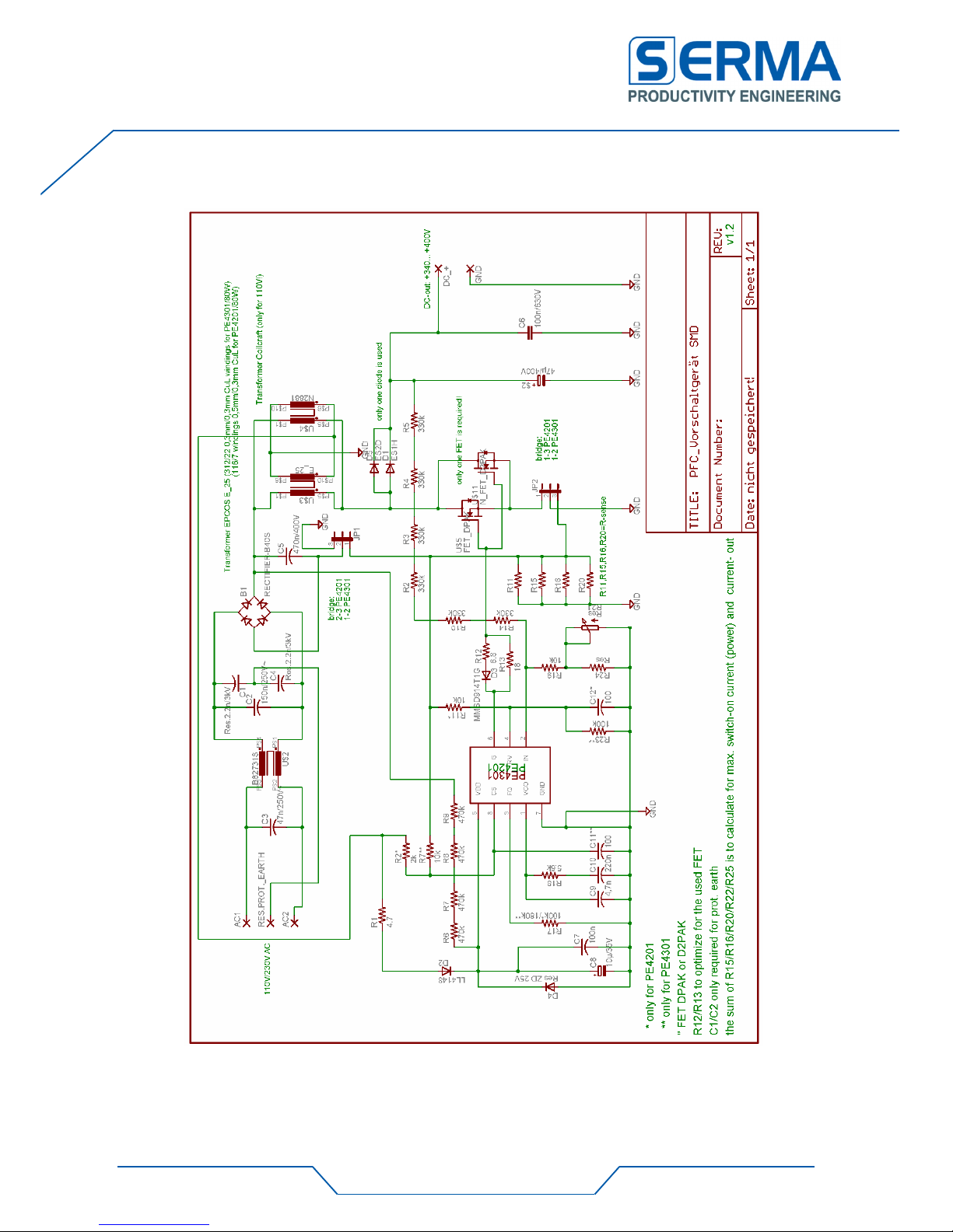
5.3 Schematic
Figure 5: Board Schematic
Page 16
ISO 9001 / ISO 14001 01/06/2016 © Productivity Engineering GmbH
Page 16 of 22
EVA4204/4301
User Guide
Evaluation Board for 80W PFC Supply
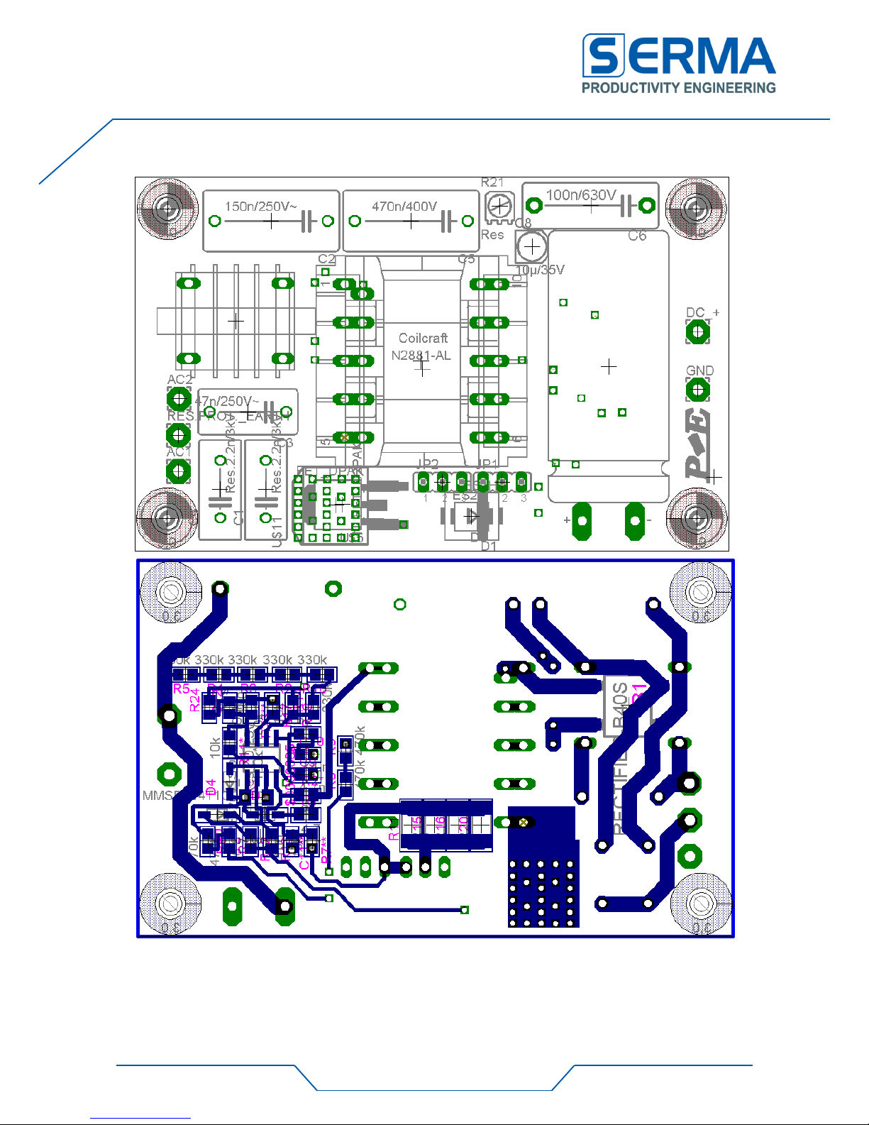
5.4 Component Placement
Figure 6: Board device population
Page 17
ISO 9001 / ISO 14001 01/06/2016 © Productivity Engineering GmbH
Page 17 of 22
EVA4204/4301
User Guide
Evaluation Board for 80W PFC Supply
5.5 Board Picture and Layout
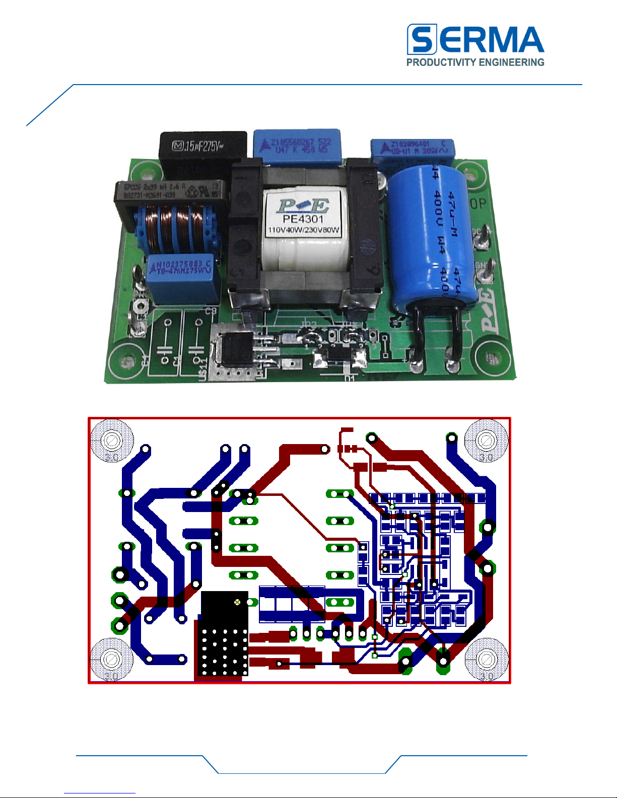
Figure 7: Board photograph (8cm x 5cm)
Figure 8: PCB Layout
Page 18

ISO 9001 / ISO 14001 01/06/2016 © Productivity Engineering GmbH
Page 18 of 22
EVA4204/4301
User Guide
Evaluation Board for 80W PFC Supply
5.6 Bill of Material
C1,C4
2
2.2n/3kV
C2N2 Res. f. Prot. Earth
C2 1 150n/250V~
C150-084X183
C3 1 47n/250V~
C102-064X133
C5 1 470n/400V
C150-084X183
C6 1 100n/630V
C15B6
C7 1 100n C1206K
C8 1 10µ/35V
153CLV
-
0405
C9 1 4,7n C0805
C10 1 220n C0805
C11** 1
100p C0805
not for
PE
4201
C12* 1 100p C0805
not for
PE
4301
C13 1 47µ/400V
VRH horizontal
D1 1 ES1H SMC
D2, D3 2 MMSD914T1G
SOD123
D4 1 Res ZD 25V
SOD123
R1 1 4.7 Ω R0805
R2, R3, R4, R5, R10, R14
6
330k R0805
R2* 1 2k R0805
not for
PE
4301
R6, R7, R8, R9
4
470k R0805
R7** 1 10k R0805
not for PE4201
R11, R19
2
10k R0805
R12 1 4.7-
6.8 Ω R0805
optimi
ze for FET
R13 1 18 - 56 Ω
R0805
optimize for FET
R11, R15, R16, R20, 4 1Ω/4.7 Ω
R0805
/R2010(PE4301)
dep. on max. power
R17 1 100k/180k
R0805
PE4201/PE
4301
R18 1 5.6k R0805
R21 1 Res (5k adjustable r.)
PC25 adjust DC
-
OUT
R23 1 100k R0805
R24 1 Re
s (tbd)
R0805
alternativ for R21
fixed
U$1 1 B40S B40S rect. 1A/400V
U$2 1 B82731S
B82731S
39mH filter
EPCOS®™
U$3 1 E_25 (EPCOS)
E25L AL=91nH/n²
U$4 1 N2881
N2881AL
Coilcraft®™
only for 110V
U$5 1 SPD07N60S5
DPAK
U$11 1 IRF840
D2PAK
$2 1 47µ/400
V VRH horizontal
$0000
1
PE4X01_SO08
PE4X01_SO08
PE4201 or PE4301
C1,C4
2
2.2n/3kV
C2N2 Res. f. Prot. Earth
C2 1 150n/250V~
C150-084X183
C3 1 47n/250V~
C102-064X133
Page 19

ISO 9001 / ISO 14001 01/06/2016 © Productivity Engineering GmbH
Page 19 of 22
EVA4204/4301
User Guide
Evaluation Board for 80W PFC Supply
6 Operating
6.1 Caution
The Evaluation board has been designed to operate between 40VAC and 80VAC input power grid
voltages and 405VDC output voltage.
Powering the board outside specified operating conditions will destroy devices and might cause severe
damage and harm people.
The board has been designed for a maximum load of 80VA. Overloading the output will cause
overheating and destruction of devices.
Devices can heat up to 50°C in normal operation mode. Take caution to not burn your fingers.
Security measures for high voltage operation have to be taken.
6.2 Load
Resistive and electronic continuous loads up to 80VA at 450VDC can be applied on the output. The load
can be applied on the DC-OUT terminal. Pay attention to the polarity and wire diameter.
6.3 AC-Input
The Input voltage has to be applied on the AC-IN terminal. An isolation transformer is required,
especially when other power grid supplied measurement devices (oscilloscope, voltmeter) are being
used to prevent from electrical shock or device damage. Avoid personal contact with the board when
powered. Be aware that capacitors hold charges even when power will be turned off. Discharge the
output capacitor through the load or a high ohmic load resistor after power off.
6.4 Power-up Sequence
Before input voltage will be turned on, all measurement devices should be connected. It is
recommended to slowly turn up the input voltage with a regulation transformer, usually in combination
with a separation transformer. Be aware that capacitors hold charges even when power will be turned
off. Make sure they will be discharged before disconnecting the measurement devices.
The board has no explicit measuring points. You can measure on the IC.
Pin of IC
7 GND: Ground, reference potential for all measuring points
5 VDD: supply voltage for PE4201/4301, 0..30VZC
8 AC (PE4201): help winding voltage through 2kOhm, -50..25V
8 CS (PE4301): negative voltage of current sensor (-0,9.. -1,2V)
3 RG (PE4201): voltage on RG, 1,03V (internal reverence)
3 FQ (PE4301): voltage on FQ, 1,03V (internal reverence)
1 VCO: voltage on output of regulation amplifier, 0 ... 5,5V
4 SH (PE4201): voltage over Shunt resistor, 0 ... 0,5V
4 RV (PE4301): adjust slew rate of the duty cycle
2 IN: voltage in loop back, V
OUT
/160, 2,50 ... 2,65V
6 G: voltage at IC-Pin G, power-MOSFET Gate driver voltage, typical 0 ...
8,5V
Vout: DCout +
Page 20

ISO 9001 / ISO 14001 01/06/2016 © Productivity Engineering GmbH
Page 20 of 22
EVA4204/4301
User Guide
Evaluation Board for 80W PFC Supply
7. List of Abbreviations
Abbreviation
Explanation
AC-IN Input Voltage
AC
Lin
Input Current
BOM
Bill of material
CCM
Con
tinuous
Conduction Mode
C
EMI
Capacitor for EMI
C
Capacity of the gate (M
O
SFET)
C
HF
Capacitor for
reduction of HF
- tran
smitting
C
Output Capacitor
C
Output Capacitor
C
SP
Cap. For
C
Cap. On Pin VDD
C
Z
Cap. On Current Sense
CRM
Critical Conduction Mode
D
BOOST
Boost
- Diode
D
Bypass
- Diode
DCM
Discontinuous
Conduction Mode
DC-OUT Output Voltage
EMI Electromagnetic Interferences
ESR Equivalent series resistance
G Output to Gate
(MOSFET)
IN
Feedback
- Input for Output
- Voltage
I
OCP
Max. Current for switching of MOSFET
I
Max. VCO
- Voltage
I
VDD
IC-
Current
L
Inductivity in CCM
L
(CRM)
In
ductivity in CRM
L
Inductor to reduce EMI
PFC Powerfactor
- Correction
P
in
Input
- Power
P
Output
- Power
PWM
Pulse- Width
- Modulation
R
Clamping Resistor
R
Start-Up Resistor
R
tFALL
Fall-Time of Voltage on Gate
R
Rise-
Time of Voltage
on Gate
THD Total Harmonic Distortion
TR Transformation Ration
t
Time for Starting the
IC
U
Gmax
Max. Voltage on Gate
VCO
Voltage Controlled
Oscillator
V
CSPCP
Voltage of
Peak
- Current
- Protection
VDD Operating Voltage of the IC
V
in
Voltage on Pi
n “IN”
V
Lock Out Voltage
V
Output Voltage
V
RREF
Internal Reference
of the IC
V
Max. Voltage on Input Current Protection
V
ST
Start UP Voltage
Page 21

ISO 9001 / ISO 14001 01/06/2016 © Productivity Engineering GmbH
Page 21 of 22
EVA4204/4301
User Guide
Evaluation Board for 80W PFC Supply
8. Notes
Page 22

ISO 9001 / ISO 14001 01/06/2016 © Productivity Engineering GmbH
Page 22 of 22
EVA4204/4301
User Guide
Evaluation Board for 80W PFC Supply
9. Contact Addresses
Germany
Stuttgart
Dresden
Productivity Engineering Productivity Engineering GmbH
Process Integration GmbH Branch
Behringstrasse 7 Sachsenallee 9
D-71083 Herrenberg D-01723 Kesselsdorf
Germany Germany
Phone.: +49 (0) 70322798 0 Phone.: +49 (0) 35204777 00
Fax: +49 (0) 70322798 29 Fax: +49 (0) 35204777 000
Email: [email protected] Email: [email protected]
Web: www.pe-gmbh.com
Im p orta n t
No tice
Productivity Engineering GmbH (PE) reserves the right to make corrections, modifications, enhancements, improvements,
and other changes to its products and services at any time and to discontinue any product or service without notice.
Customers should obtain the latest relevant information before placing orders and should verify that such information is
current and complete. All products are sold subject to PE’s terms and conditions of sale supplied at the time of order
acknowledgment. PE warrants performance of its hardware products to the specifications applicable at the time of sale in
accordance with PE’s standard warranty. Testing and other quality control techniques are used to the extent PE deems
necessary to support this warranty. Except where mandated by government requirements, testing of all parameters of each
product is not necessarily performed. PE assumes no liability for applications assistance or customer product design.
Customers are responsible for their products and applications using PE components. To minimize the risks associated with
customer products and applications, customers should provide adequate design and operating safeguards. PE does not
warrant or represent that any license, either express or implied, is granted under any PE patent right, copyright, mask work
right, or other PE intellectual property right relating to any combination, machine, or process in which PE products or services
are used. Information published by PE regarding third–party products or services does not constitute a license from PE to
use such products or services or a warranty or endorsement thereof. Use of such information may require a license from a
third party under the patents or other intellectual property of the third party, or a license from PE under the patents or other
intellectual property of PE. Resale of PE products or services with statements different from or beyond the parameters stated
by PE for that product or service voids all express and any implied warranties for the associated PE product or service and is
an unfair and deceptive business practice. PE is not responsible or liable for any such statements.
© 2016 PE GmbH. All rights reserved.
All trademarks and registered trademarks are the property of their respective owners.
The project is funded in parts by the European fund for regional development (EFRE) and the state of Saxony.
 Loading...