

Page 1

Sequans Module VZM20Q
SEQUANS Communications
15-55, Boulevard Charles de Gaulle
92700 Colombes, France
Phone. +33.1.70.72.16.00
Fax. +33.1.70.72.16.09
www.sequans.com
contact@sequans.com
Module
Integration
Guide
Page 2

Legal Notices
Copyright© 2016, SEQUANS Communications
All information contained herein and disclosed by this document is
confidential and the proprietary property of SEQUANS Communications,
and all rights therein are expressly reserved. Acceptance of this material
signifies agreement by the recipient that the information contained in this
document is confidential and that it will be used solely for the purposes set
forth herein. Acceptance of this material signifies agreement by the recipient
that it will not be used, reproduced in whole or in part, disclosed, distributed,
or conveyed to others in any manner or by any means – graphic, electronic, or
mechanical, including photocopying, recording, taping, or information
storage and retrieval systems – without the express written permission of
SEQUANS Communications.
Preface
All Sequans’ logos and trademarks are the property of SEQUANS
Communications. Unauthorized usage is strictly prohibited without the
express written permission of SEQUANS Communications. All other
company and product names may be trademarks or registered trademarks of
their respective owners. Products and services of SEQUANS
Communications, and those of its licensees may be protected by one or more
pending or issued U.S. or foreign patents.
Because of continuing developments and improvements in design,
manufacturing, and deployment, material in this document is subject to
change without notification and does not represent any commitment or
obligation on the part of SEQUANS Communications. SEQUANS
Communications shall have no liability for any error or damages resulting
from the use of this document.
MODULE INTEGRATION GUIDE PROPRIETARY i
SEQUANS Communications
Page 3

Document Revision History
Revision Date Product Application
01 November 2016 First edition of the VZM20Q Module Integration Guide.
ii PROPRIETARY MODULE INTEGRATION GUIDE
SEQUANS Communications
Page 4

Purpose and Scope
This Application note is intended to help customers who want to deviate from
the Sequans’ Reference Designs to successfully integrate and test their
product based on module.
It presents Integration Guidelines for:
• All VZM20Q Interface Requirements
• Tips and “how-to”s for troubleshooting
Development of the Hardware should follow a process that ensures the
solution will be optimum and it is the purpose / goal of this document to reach
this. For this to occur it is recommended that these processes are followed in
order. This document is delivered as three sections:
About this Guide
1. System Overview
2. Hardware and software design guidelines
3. Bring-up verification and test
Caution: It is highly recommended that Sequans support teams are
involved during all processes to ensure the very best can be
achieved for the alternative design.
Who Should Read this Document
This Application Note is for hardware designers of user applications based on
Sequans VZM20Q Module.
Important: Reference design source files are based on the application PADS®
from Mentor Graphics® (www.mentor.com). Customers using
the other CAD applications can use schematics translators and
viewers, such as Elgris® (www.elgris.com). Such translators may
save time and prevent mistakes during manual PADs conversion.
MODULE INTEGRATION GUIDE PROPRIETARY iii
SEQUANS Communications
Page 5

Reference Documentation
1. DV Tool User Guide
2. Sequans Hardware Platform User Guide
3. mTools Reference Manual
4. Nimbelink™ Evaluation Kit User Manual
See http://nimbelink.com/
Changes in this Document
This is the first edition of the document.
iv PROPRIETARY MODULE INTEGRATION GUIDE
SEQUANS Communications
Page 6
Documentation Conventions
This section illustrates the conventions that are used in this document.
General Conventions
Note Important information requiring the user’s attention.
A condition or circumstance that may cause damage to the equipment or loss of
data.
Caution
A condition or circumstance that may cause personal injury.
War ning
Italics Italic font style denotes
• emphasis of an important word;
• first use of a new term;
• title of a document.
Screen Name Sans serif, bold font denotes
• on-screen name of a window, dialog box or field;
• keys on a keyboard;
• labels printed on the equipment.
Software Conventions
Code Regular Courier font denotes code or text displayed on-screen.
Code Bold Courier font denotes commands and parameters that you enter exactly as
shown. Multiple parameters are grouped in brackets [ ]. If you are to choose only
one among grouped parameters, the choices are separated with a pipe: [parm1 |
parm2 | parm3] If there is no pipe separator, you must enter each parameter:
[parm1 parm2 parm3]
Code Italic Courier font denotes parameters that require you to enter a value or
variable. Multiple parameters are grouped in brackets [ ]. If you are to choose
only one among grouped parameters, the choices are separated with a pipe:
[parm1 | parm2 | parm3] If there is no pipe separator, you must enter a value for
each parameter: [parm1 parm2 parm3]
MODULE INTEGRATION GUIDE PROPRIETARY v
SEQUANS Communications
Page 7

Table of Contents
Preface . . . . . . . . . . . . . . . . . . . . . . . . . . . . . . . . . . . . . . i
Legal Notices . . . . . . . . . . . . . . . . . . . . . . . . . . . . . . . . . . . . . . . . . . . . . . . . . . . . . . . . . . . . . . . . . . . . . . .i
Document Revision History. . . . . . . . . . . . . . . . . . . . . . . . . . . . . . . . . . . . . . . . . . . . . . . . . . . . . . . . . . .ii
About this Guide . . . . . . . . . . . . . . . . . . . . . . . . . . . . . . . . . iii
Purpose and Scope . . . . . . . . . . . . . . . . . . . . . . . . . . . . . . . . . . . . . . . . . . . . . . . . . . . . . . . . . . . . . . . . . iii
Who Should Read this Document . . . . . . . . . . . . . . . . . . . . . . . . . . . . . . . . . . . . . . . . . . . . . . . . . . . . . iii
Reference Documentation . . . . . . . . . . . . . . . . . . . . . . . . . . . . . . . . . . . . . . . . . . . . . . . . . . . . . . . . . . . .iv
Changes in this Document . . . . . . . . . . . . . . . . . . . . . . . . . . . . . . . . . . . . . . . . . . . . . . . . . . . . . . . . . . . .iv
Documentation Conventions . . . . . . . . . . . . . . . . . . . . . . . . . . . . . . . . . . . . . . . . . . . . . . . . . . . . . . . . . . v
Chapter 1
Introduction . . . . . . . . . . . . . . . . . . . . . . . . . . . . . . . . . . . 1
1.1 System Architecture . . . . . . . . . . . . . . . . . . . . . . . . . . . . . . . . . . . . . . . . . . . . . . . . . . . . . . 1
1.2 Recommended Design Flow. . . . . . . . . . . . . . . . . . . . . . . . . . . . . . . . . . . . . . . . . . . . . . . . 3
1.2.1 Design Modifications . . . . . . . . . . . . . . . . . . . . . . . . . . . . . . . . . . . . . . . . . . . . . . . . . 3
1.2.2 Schematics Review . . . . . . . . . . . . . . . . . . . . . . . . . . . . . . . . . . . . . . . . . . . . . . . . . . . 3
1.2.3 PCB Placement and Layout Review . . . . . . . . . . . . . . . . . . . . . . . . . . . . . . . . . . . . . . 3
1.2.4 Optimization . . . . . . . . . . . . . . . . . . . . . . . . . . . . . . . . . . . . . . . . . . . . . . . . . . . . . . . . 4
1.2.5 Functional Validation . . . . . . . . . . . . . . . . . . . . . . . . . . . . . . . . . . . . . . . . . . . . . . . . . 4
1.2.6 Manufacturing Recommended Process . . . . . . . . . . . . . . . . . . . . . . . . . . . . . . . . . . . 4
Chapter 2
Manufacturing Process . . . . . . . . . . . . . . . . . . . . . . . . . . . . . 5
2.1 Manufacturing Process Overview. . . . . . . . . . . . . . . . . . . . . . . . . . . . . . . . . . . . . . . . . . . . 5
2.2 Module Upgrade . . . . . . . . . . . . . . . . . . . . . . . . . . . . . . . . . . . . . . . . . . . . . . . . . . . . . . . . . 5
Chapter 3
Hardware Integration Recommendations . . . . . . . . . . . . . . . . . . . 6
3.1 Power Supply . . . . . . . . . . . . . . . . . . . . . . . . . . . . . . . . . . . . . . . . . . . . . . . . . . . . . . . . . . . 7
3.1.1 Synthesis of the Power Supplies . . . . . . . . . . . . . . . . . . . . . . . . . . . . . . . . . . . . . . . . . 7
3.1.2 Power Supply Circuit Example . . . . . . . . . . . . . . . . . . . . . . . . . . . . . . . . . . . . . . . . . 8
3.1.3 Module Operating Mode . . . . . . . . . . . . . . . . . . . . . . . . . . . . . . . . . . . . . . . . . . . . . . 8
3.2 SIM Interface . . . . . . . . . . . . . . . . . . . . . . . . . . . . . . . . . . . . . . . . . . . . . . . . . . . . . . . . . . . 8
3.2.1 Interface Description . . . . . . . . . . . . . . . . . . . . . . . . . . . . . . . . . . . . . . . . . . . . . . . . . 8
3.2.2 Other Hardware Considerations . . . . . . . . . . . . . . . . . . . . . . . . . . . . . . . . . . . . . . . . . 9
3.2.3 Software-Configurable Options . . . . . . . . . . . . . . . . . . . . . . . . . . . . . . . . . . . . . . . . . 9
3.3 Host Communications Signals . . . . . . . . . . . . . . . . . . . . . . . . . . . . . . . . . . . . . . . . . . . . . . 9
Proprietary vi
SEQUANS Communications
Page 8

Table of Contents
3.3.1 Introduction to UART Interfaces . . . . . . . . . . . . . . . . . . . . . . . . . . . . . . . . . . . . . . . . 9
3.3.2 General Notes on UART Connections . . . . . . . . . . . . . . . . . . . . . . . . . . . . . . . . . . . 10
3.3.3 UART0 Interface . . . . . . . . . . . . . . . . . . . . . . . . . . . . . . . . . . . . . . . . . . . . . . . . . . . 11
3.3.4 UART1 Interface . . . . . . . . . . . . . . . . . . . . . . . . . . . . . . . . . . . . . . . . . . . . . . . . . . . 12
3.3.5 UART2 Interface . . . . . . . . . . . . . . . . . . . . . . . . . . . . . . . . . . . . . . . . . . . . . . . . . . . 13
3.4 RF Interface . . . . . . . . . . . . . . . . . . . . . . . . . . . . . . . . . . . . . . . . . . . . . . . . . . . . . . . . . . . 15
3.4.1 RF Signals . . . . . . . . . . . . . . . . . . . . . . . . . . . . . . . . . . . . . . . . . . . . . . . . . . . . . . . . . 15
3.4.2 Circuit Diagram Example . . . . . . . . . . . . . . . . . . . . . . . . . . . . . . . . . . . . . . . . . . . . . 16
3.4.3 Test Points and Measurement Access . . . . . . . . . . . . . . . . . . . . . . . . . . . . . . . . . . . 17
3.4.4 Antennas and RF Design Considerations . . . . . . . . . . . . . . . . . . . . . . . . . . . . . . . . . 17
3.5 Reset and Environmental Signals . . . . . . . . . . . . . . . . . . . . . . . . . . . . . . . . . . . . . . . . . . . 20
3.6 GPIO Control Interface. . . . . . . . . . . . . . . . . . . . . . . . . . . . . . . . . . . . . . . . . . . . . . . . . . . 21
3.6.1 Interface Description . . . . . . . . . . . . . . . . . . . . . . . . . . . . . . . . . . . . . . . . . . . . . . . . 21
3.6.2 Software Configurable Options . . . . . . . . . . . . . . . . . . . . . . . . . . . . . . . . . . . . . . . . 22
Chapter 4
PCB Layout Rules . . . . . . . . . . . . . . . . . . . . . . . . . . . . . . . 23
4.1 Placement . . . . . . . . . . . . . . . . . . . . . . . . . . . . . . . . . . . . . . . . . . . . . . . . . . . . . . . . . . . . . 23
4.2 Trace Characteristic Design . . . . . . . . . . . . . . . . . . . . . . . . . . . . . . . . . . . . . . . . . . . . . . . 24
4.2.1 Digital Traces . . . . . . . . . . . . . . . . . . . . . . . . . . . . . . . . . . . . . . . . . . . . . . . . . . . . . . 24
4.2.2 Power Supply Traces . . . . . . . . . . . . . . . . . . . . . . . . . . . . . . . . . . . . . . . . . . . . . . . . 24
4.2.3 RF Traces . . . . . . . . . . . . . . . . . . . . . . . . . . . . . . . . . . . . . . . . . . . . . . . . . . . . . . . . . 25
4.2.4 Controlled Impedance Traces . . . . . . . . . . . . . . . . . . . . . . . . . . . . . . . . . . . . . . . . . . 25
4.2.5 Grounding . . . . . . . . . . . . . . . . . . . . . . . . . . . . . . . . . . . . . . . . . . . . . . . . . . . . . . . . . 26
Chapter 5
Bring-Up and Testing . . . . . . . . . . . . . . . . . . . . . . . . . . . . . 27
5.1 Introduction. . . . . . . . . . . . . . . . . . . . . . . . . . . . . . . . . . . . . . . . . . . . . . . . . . . . . . . . . . . . 27
5.2 Prerequisites . . . . . . . . . . . . . . . . . . . . . . . . . . . . . . . . . . . . . . . . . . . . . . . . . . . . . . . . . . . 27
5.3 Functional Verification without Assembled Module . . . . . . . . . . . . . . . . . . . . . . . . . . . . 28
5.3.1 Power Supply . . . . . . . . . . . . . . . . . . . . . . . . . . . . . . . . . . . . . . . . . . . . . . . . . . . . . . 28
5.3.2 RF Path . . . . . . . . . . . . . . . . . . . . . . . . . . . . . . . . . . . . . . . . . . . . . . . . . . . . . . . . . . . 30
5.4 Functional Verification with Assembled Module. . . . . . . . . . . . . . . . . . . . . . . . . . . . . . . 31
5.4.1 Power Supply . . . . . . . . . . . . . . . . . . . . . . . . . . . . . . . . . . . . . . . . . . . . . . . . . . . . . . 31
5.4.2 Confirm Module Power-Up Operation (UART1) . . . . . . . . . . . . . . . . . . . . . . . . . . 32
5.4.3 GPIOs . . . . . . . . . . . . . . . . . . . . . . . . . . . . . . . . . . . . . . . . . . . . . . . . . . . . . . . . . . . . 33
5.4.4 SIM Communication . . . . . . . . . . . . . . . . . . . . . . . . . . . . . . . . . . . . . . . . . . . . . . . . 34
5.5 LTE RF Performance Test . . . . . . . . . . . . . . . . . . . . . . . . . . . . . . . . . . . . . . . . . . . . . . . . 35
5.5.1 Test Configuration . . . . . . . . . . . . . . . . . . . . . . . . . . . . . . . . . . . . . . . . . . . . . . . . . . 35
5.5.2 Procedure . . . . . . . . . . . . . . . . . . . . . . . . . . . . . . . . . . . . . . . . . . . . . . . . . . . . . . . . . 36
5.5.3 Troubleshooting . . . . . . . . . . . . . . . . . . . . . . . . . . . . . . . . . . . . . . . . . . . . . . . . . . . . 36
Appendix A
Hardware Test Preparation . . . . . . . . . . . . . . . . . . . . . . . . . . 37
A.1 RF Interfaces Preparation . . . . . . . . . . . . . . . . . . . . . . . . . . . . . . . . . . . . . . . . . . . . . . . . . 37
Proprietary vii
SEQUANS Communications
Page 9

Table of Contents
A.1.1 LTE RF Test Preparation . . . . . . . . . . . . . . . . . . . . . . . . . . . . . . . . . . . . . . . . . . . . . 37
Appendix B
Abbreviations . . . . . . . . . . . . . . . . . . . . . . . . . . . . . . . . . . 40
viii Proprietary M
SEQUANS Communications
ODULE INTEGRATION GUIDE
Page 10
Introduction
,K^dW>d&KZD
sDϮϬY
Z&
ŽĂdž
/&dž
Zydy
sd
sϭͺW
sϮͺW
sdϭ
Z^dE
DKh>ͺKE
:d '
^/D
hZdϭ;KƉƚŝŽŶĂůͿ
DŽĚĞŵ/ŶƚĞƌĨĂĐĞ;hZdϬͿ
'W/K
ϯsϬ
ĞďƵŐ;hZdϮͿ
;ĞďƵŐDĂŶƵĨĂĐƚƵƌŝŶŐĐŽŶƐŽůĞͿ
1
1.1 System Architecture
Figure 1-1 provides an overview of the Host to VZM20Q interfacing
relationship. The various interfaces are explained in detail later in this
document.
It provides summary details of:
• Digital interfaces between the VZM20Q and the host platform
• Power supply requirement (V
Note: V
It does not show the VZM20Q local terminations.
range is 3.1 V to 4.5 V.
BAT1
bat
).
MODULE INTEGRATION GUIDE PROPRIETARY 1
Figure 1-1: VZM20Q-Based System Architecture
SEQUANS Communications
Page 11
INTRODUCTION
SYSTEM ARCHITECTURE
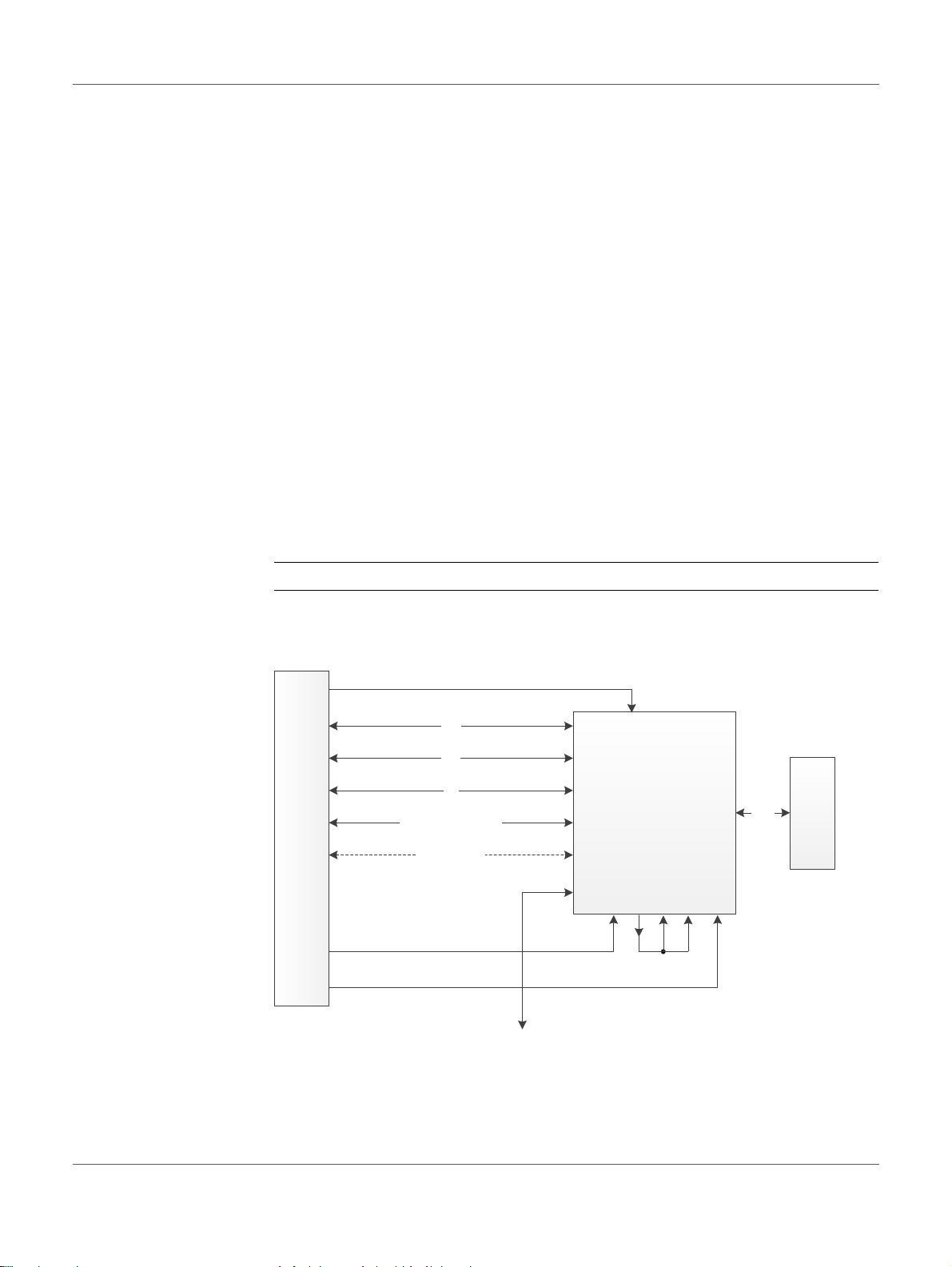
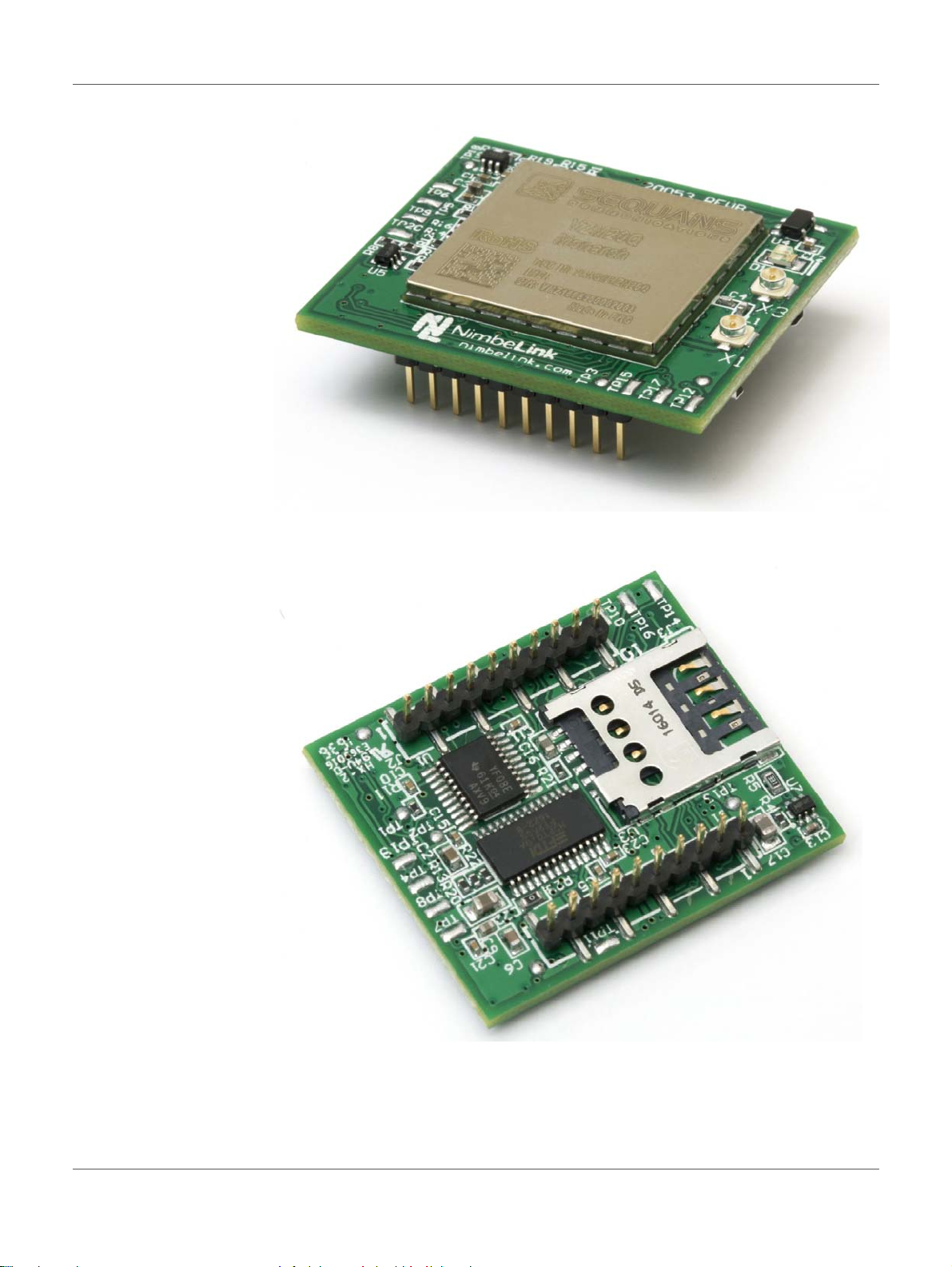
Figure 1-2: VZM20Q Mounted on Skywire™ 4G LTE CAT M1 Embedded
Modem
Figure 1-3: Skywire™ 4G LTE CAT M1 Embedded Modem - Bottom View
2 PROPRIETARY MODULE INTEGRATION GUIDE
SEQUANS Communications
Page 12

Note: The hardware design package of VZM20Q reference design is
available from your Sequans local contact.
1.2 Recommended Design Flow
To ensure that the customer benefits from the details of this document we
recommend to carefully take the following information into account during
the design process.
1.2.1 Design Modifications
Compared to Nimbelink™ reference design, only the following modifications
to the BOM are allowed to designers:
INTRODUCTION
RECOMMENDED DESIGN FLOW
• SIM connector
•Level shifter on UARTs
• Circuitry on RESETN
Note: Any GNSS/GPS function is out of scope of VZM20Q Reference
Design.
Consultancy with Sequans is highly recommended to verify these alternate
preferences.
1.2.2 Schematics Review
Ensuring that the circuit design by analysis will be compliant with the
Sequans’ chipset. It is recommended that the review of the design includes
Sequans’ technical support team.
1.2.3 PCB Placement and Layout Review
To ensure the PCB layout is compliant, it is recommended that the review of
this CAD activity includes Sequans at several iterative steps such as
component placement, RF and digital routing, final layout levels etc. This
might avoid later rework.
MODULE INTEGRATION GUIDE PROPRIETARY 3
SEQUANS Communications
Page 13

INTRODUCTION
RECOMMENDED DESIGN FLOW
1.2.4 Optimization
When the design returns from the manufacture, it might occur that
improvements have to be made to the circuits. It is also recommended to
communicate such results to Sequans who can help to verify the
implementation.
1.2.5 Functional Validation
The test of the design performance should be done in thorough detail. This
will ensure the compliance with the test standard as the final design will be
subjected to a formal qualification. It is the designer’s responsibility to meet
this goal. Sharing the results with Sequans will help identify any particular
problem that could be fixed at an early stage to ensure strong confidence of
qualification. This should be done for all the tests that involve Sequans
chipsets.
Hardware Test Preparation on page 37 provides you with the hardware setup
required to proceed with test phases.
1.2.6 Manufacturing Recommended Process
Manufacturing Process on page 5 provides information on the process
required to achieve the manufacturing of your product.
4 PROPRIETARY MODULE INTEGRATION GUIDE
SEQUANS Communications
Page 14

Manufacturing Process
2
2.1 Manufacturing Process Overview
Note: The contents of this section will be provided in a future revision
of the document.
2.2 Module Upgrade
Note: The contents of this section will be provided in a future revision
of the document.
MODULE INTEGRATION GUIDE PROPRIETARY 5
SEQUANS Communications
Page 15

Hardware Integration Recommendations
3
This chapter provides the information necessary to understand the various
interface requirements to interconnect with the VZM20Q, associated
software-configurable items for the respective interface and, more generally,
good practices for board design when considering the various interface types.
Table 3-1 describes the requirements for trace characteristics.
Important: Different signals require different special needs. Please consider
carefully the interfacing requirement of each relevant connection.
Table 3-1: Requirements Overview: Trace Characteristics
Trace Characteristics Description
Digital Generic digital trace if reasonable high impedance
Supply Broader trace routing based on the power needs of the load
50 Ohm Conventionally used for RF routing. Track must be retained to this impedance
Quiet Intention is to keep away from digital signals and as short as possible, possibly burying
the signal
Ground Shortest VZM20Q Ground to Host Ground possible, best possible lowest impedance
path
MODULE INTEGRATION GUIDE PROPRIETARY 6
SEQUANS Communications
Page 16

HARDWARE INTEGRATION RECOMMENDATIONS
3.1 Power Supply
3.1.1 Synthesis of the Power Supplies
Table 3-2 and Table 3- 3 provide a synthesis of the power supplies and their
characteristics. Please see typical voltage values in VZM20Q Datasheet.
Note: Each output reference voltage (pads 3, 9, 11) can be either running
or powered off depending on the internal software configuration.
They should not be used to power external IC or parts that require
permanent supply.
Table 3-2: Power Supply Signals
POWER SUPPLY
Pin
Pin Name
1V8 3 Supply Out Reference voltage. See the note above.
3V0 9,11 Supply Out To be only connected to VCC1_PA and VCC2_PA. These pads
GNSS_VCC1 100 Supply In Reserved. Do not connect.
GNSS_VCC2 101 Supply Out Reserved. Do not connect.
GNSS_VCC3 102 Supply In Reserved. Do not connect.
VBAT1 107, 108 Supply In Voltage used for qualification is 3.8 V, range 3.1 V to 4.5 V
VCC1_PA 97 Supply In To be connected to 3V0
VCC2_PA 98, 99 Supply In To be connected to 3V0
Number
Trace
Style
Direction Notes
should not be used for any other usage. See the note above.
Table 3-3: Power Supply Digital Enable Signals
Typical
Pin
Pin Name
POWER_EN 106 Digital In 1V8
MODULE INTEGRATION GUIDE PROPRIETARY 7
Number
Tra ce
Style
SEQUANS Communications
Direction
Voltage
Ref
Notes
Page 17

HARDWARE INTEGRATION RECOMMENDATIONS
SIM INTERFACE
3.1.2 Power Supply Circuit Example
3.1.2.1 Test Points and Measurement Access
Test point access is recommended on all supply nets so that the supply
voltages can be measured.
3.1.2.2 Special Layout Considerations
PLease refer to Section 4.2.2 Power Supply Traces on page 24.
3.1.3 Module Operating Mode
Note: The contents of this section will be provided in a future revision
of the document.
3.2 SIM Interface
3.2.1 Interface Description
Table 3-4 lists the VZM20Q pins related to the SIM interface.
Table 3-4: SIM Interface Signals
Pin
Pin Name
SIM_CLK 14 Digital Output from Module SIM_VCC
SIM_DETECT
SIM_IO 17 Digital Input or Output to/from Module SIM_VCC
SIM_RESETN 12 Digital Output from Module SIM_VCC
SIM_VCC 18 Digital Output from Module 1V8 or 3V0
1
Number
16 Digital Input to Module 1V8
Trace Style Direction
Electrical
Characteristics
1. SIM_DETECT=1 signals that a card is present. SIM_DETECT=0 signals that no card is present.
8 PROPRIETARY MODULE INTEGRATION GUIDE
SEQUANS Communications
Page 18

HARDWARE INTEGRATION RECOMMENDATIONS
3.2.2 Other Hardware Considerations
• When considering the placement of the SIM connector and Monarch SIM
interface, try to keep the distance between them as small as possible. This
is to avoid supply trace inductance buildup which could cause unexpected
SIM VCC supply drops under specific SIM control situations. If it is
unavoidable, then be sure to add 4.7µF decoupling capacitor at the SIM
connector itself to act as a charge reserve in help in such situations.
• Please ensure that a good ground return exists between the SIM card and
the VZM20Q.
• If the application requires the support of the hot insertion or removal of
SIM card, then the SIM card handler must include a removal/insertion pad
detector in order to allow the software to process the event immediately.
• The software support of the “hot removal” feature is not currently available. Please contact your Sequans’ representative for details.
3.2.3 Software-Configurable Options
HOST COMMUNICATIONS SIGNALS
Note: The content of this section will be provided in a future revision of
the document.
3.3 Host Communications Signals
3.3.1 Introduction to UART Interfaces
The communication between the VZM20Q and the host platform is supported
as follows by 3 UART interfaces.
• UART0 is dedicated to Host-Modem interface
• UART1 is an optional additional Host-Modem interface. It is reserved for
future use.
• UART2 is reserved for debug usage and Sequans’ manufacturing and hardware qualification tools such as DMTool or DVTool.
The following sections detail those interfaces.
MODULE INTEGRATION GUIDE PROPRIETARY 9
SEQUANS Communications
Page 19

HARDWARE INTEGRATION RECOMMENDATIONS
sDϮdžY
ƉƉůŝĐĂƚŝŽŶ
dyϬϭϮ dy
ZyϬϭϮ Zy
Zd^ϬϭϮ Zd^
d^ϬϭϮ d^
><ϬϭϮ ><
dZϬ dZ
^ZϬ ^Z
Ϭ
Z/E'Ϭ Z/E'
HOST COMMUNICATIONS SIGNALS
3.3.2 General Notes on UART Connections
VZM20Q uses the DCE-DTE convention for UART lines.
The TXD output from the device at one end of the link connects to the RXD
input at the other end of the link and vice versa. Figure 3-1 represents the
typical implementation for the UART connection (including hardware flow
control in case of high-speed UART).
TXD and RXD signals are mandatory for all interfaces. The other signals are
optional. Only UART0 interface supports all data transfer signals.
The DCE (Data Communication Equipment) device will communicate with
the customer application (DTE) using the following signals:
• Port TXD on Application sends data to the VZM20Q's TXD signal line.
• Port RXD on Application receives data from the VZM20Q's RXD signal
line.
Figure 3-1: UART0, UART1, UART2 Connection Implementation
10 PROPRIETARY MODULE INTEGRATION GUIDE
SEQUANS Communications
Page 20

3.3.3 UART0 Interface
3.3.3.1 Interface Description
Important:
• See the Section 3.3.2 General Notes on UART Connections on
page 10 for usage of UART0.
• If not used, the UART0 signals should be connected to test
points.
Table 3-4 lists the VZM20Q pins related to the UART0 interface.
Table 3-5: UART Interface Signals
HARDWARE INTEGRATION RECOMMENDATIONS
HOST COMMUNICATIONS SIGNALS
Pin
Pin Name
RXD0 79 Digital Out 1.8 V UART0 RXD
TXD0 77 Digital In 1.8 V UART0 TXD
RTS0 75 Digital In 1.8 V UART0 RTS
CTS0 76 Digital Out 1.8 V UART0 CTS
GPIO19/CLK0 7 Digital In/Out 1.8 V UART0 CLK optional signal multiplexed
GPIO41/DTR0 84 Digital In 1.8 V UART0 DTR optional signal multiplexed
GPIO39/DSR0 85 Digital Out 1.8 V UART0 DSR optional signal multiplexed
GPIO24/DCD0 88 Digital Out 1.8 V UART0 DCD optional signal multiplexed
GPIO25/RING0 89 Digital Out 1.8 V UART0 RING optional signal multiplexed
Number
Trace
Style
Direction
Electrical
Characteristics
Notes
with GPIO19. Default setting is GPIO.
with GPIO41. Default setting is GPIO.
with GPIO39. Default setting is GPIO.
with GPIO24. Default setting is GPIO.
with GPIO25. Default setting is GPIO.
MODULE INTEGRATION GUIDE PROPRIETARY 11
SEQUANS Communications
Page 21

HARDWARE INTEGRATION RECOMMENDATIONS
HOST COMMUNICATIONS SIGNALS
3.3.3.2 Default Configuration
The default software configuration of UART0 is AT Commands mode.
The serial link settings are as follows:
• Baud rate: 921600
• Data: 8 bits
•Parity: None
• Stop : 1 bit
• Flow control: Hardware (RTS/CTS)
3.3.4 UART1 Interface
3.3.4.1 Interface Description
Important:
• See the Section 3.3.2 General Notes on UART Connections on
page 10 for usage of UART1.
• If not used, the UART1 signals should be connected to test
points.
Table 3-6 lists the VZM20Q pins related to the UART1 interface.
Table 3-6: UART1 Interface Signals
Pin
Pin Name
GPIO15/RXD1 80 Digital Out 1.8 V UART1 RXD optional signal multiplexed
GPIO14/TXD1 78 Digital In 1.8 V UART1 TXD optional signal multiplexed
GPIO16/RTS1 83 Digital In 1.8 V UART1 RTS optional signal multiplexed
GPIO17/CTS1 81 Digital Out 1.8 V UART1 CTS optional signal multiplexed
Number
Trace
Style
Direction
Electrical
Characteristics
Notes
with GPIO15. Default setting is RXD1.
with GPIO14. Default setting is TXD1.
with GPIO16. Default setting is GPIO.
with GPIO17. Default setting is GPIO.
GPIO38/CLK1 82 Digital In/Out 1.8 V UART1 CLK optional signal multiplexed
with GPIO38. Default setting is GPIO.
12 PROPRIETARY MODULE INTEGRATION GUIDE
SEQUANS Communications
Page 22

3.3.4.2 Default Configuration
The default software configuration of UART1 is console mode. Boot traces are
sent on this interface as shown on Section 5.4.2 Confirm Module Power-Up
Operation (UART1) on page 32.
The serial link settings are as follows:
• Baud rate: 115200
• Data: 8 bits
•Parity: None
• Stop : 1 bit
•Flow control: None
3.3.5 UART2 Interface
HARDWARE INTEGRATION RECOMMENDATIONS
HOST COMMUNICATIONS SIGNALS
3.3.5.1 Interface Description
Important:
• See the Section 3.3.2 General Notes on UART Connections on
page 10 for usage of UART2.
• If not used, the UART2 signals should be connected to test
points.
Table 3-7 lists the VZM20Q pins related to the UART2 interface.
Table 3-7: UART2 Interface Signals
Pin
Pin Name
RXD2 56 Digital Out 1.8 V UART2 RXD.
TXD2 58 Digital In 1.8 V UART2 TXD
GPIO28/RTS2 10 Digital In 1.8 V UART2 RTS optional signal multiplexed
Number
Trace
Style
Direction
Electrical
Characteristics
Notes
with GPIO28. Default setting is RTS.
GPIO27/CTS2 8 Digital Out 1.8 V UART2 CTS optional signal multiplexed
with GPIO27. Default setting is CTS.
GPIO26/CLK2 91 Digital In/Out 1.8 V UART2 CLK optional signal multiplexed
with GPIO26. Default setting is GPIO
MODULE INTEGRATION GUIDE PROPRIETARY 13
SEQUANS Communications
Page 23

HARDWARE INTEGRATION RECOMMENDATIONS
HOST COMMUNICATIONS SIGNALS
3.3.5.2 Default Configuration
UART2 default software configuration allows firmware upload when the
device is configured in FFH mode, then it switchs in debug mode (enabling
DVTool, DMTool).
The serial link settings are as follows:
• Baud rate: 921600
• Data: 8 bits
•Parity: None
• Stop : 1 bit
• Flow control: Hardware (RTS/CTS)
14 PROPRIETARY MODULE INTEGRATION GUIDE
SEQUANS Communications
Page 24

3.4 RF Interface
3.4.1 RF Signals
3.4.1.1 RF Interface Signals
Table 3-8: RF Interface Signals
HARDWARE INTEGRATION RECOMMENDATIONS
RF INTERFACE
Pin
Name
LTE_ANT0 54 RF In/Out RF LTE antenna. Special RF routing conditions
GNSS_ANT1 44 Reserved Reserved. Do not connect.
Pin
Number
Tra ce
Style
Direction
Electrical
Characteristics
Notes
3.4.1.2 RF Control Signals
Table 3-9: RF Control Signals
Pin
Name
RFDATA12 39 Digital In/Out Reserved.
RFDATA16 40 Digital In/Out Reserved.
RFDATA17 41 Digital In/Out Reserved.
Pin
Number
Tra ce
Style
Direction
Electrical
Characteristics
Notes
MODULE INTEGRATION GUIDE PROPRIETARY 15
SEQUANS Communications
Page 25

HARDWARE INTEGRATION RECOMMENDATIONS
RF INTERFACE
3.4.2 Circuit Diagram Example
Important: Figure 3-4 should be strictly followed as a topology reference. It is
recommended not to deviate from this circuit from your application. More information is provided in this document on the layout
constraint which are too very important to abide by.
The RF inter-connect called P1 is for example purposes only. Depending on
the antenna, interfacing system will dictate the RF inter-connect.
Figure 3-2: RF Typical Circuit
LTE_ANT0 is the primary (main) antenna pin and carries TX and RX signals.
Connect 50 Ohm transmission lines from this pins to the 50 Ohm Primary
Antenna/Antenna-connector.
Figure 3-2 shows, included in the connection between ANT and the antenna
connectors, T-type network for matching.
See Section 3.4.4 Antennas and RF Design Considerations on page 17 for more
detail on connecting to these pins and for information on the T-type matching
network and ESD protection.
16 PROPRIETARY MODULE INTEGRATION GUIDE
SEQUANS Communications
Page 26

HARDWARE INTEGRATION RECOMMENDATIONS
3.4.3 Test Points and Measurement Access
50 Ohm termination points, for example P1 in Figure 3-2, are needed for
Engineering and Production teams for the validation of the RF performance.
The potential need to optimize the Pi-type matching network in the antenna
path means that access to the IOs of this matching network is needed, so that a
coaxial cable (usually 1.25mm diameter semi-rigid) can be manually attached
for precision impedance measurements. Critically, a sufficient area of GND
metal on the top layer adjacent to these matching networks and
well-grounded to the transmission line reference GND is needed to permit
robust physical attachment of the coaxial cable and with short GND
connection. This area of GND metal does not need any resist removal as this
can be removed manually where needed.
Please refer to Section 3.4.4 Antennas and RF Design Considerations on page 17 for more detail on managing RF Trace Design.
RF INTERFACE
3.4.4 Antennas and RF Design Considerations
Antennas require special interfacing for optimum RX and TX Performance.
3.4.4.1 T-Type Matching
A 3-component T-type matching network is recommended to be fitted. The
purpose of the T-type matching network is to transform the impedance of the
RF-path that extends beyond to 50 Ohm if needed. The 3 components in this
matching network should be as close together as possible to minimise the
interconnecting track lengths.
By default the component pads should be for a 0201-size capacitor which can
be a No Fit by default. There should be a short low-impedance connection
connecting the GND node of this component.
The series matching element should be connected at the junction where first
shunt component and by default a 0 Ohm 0201-size resistor should be fitted
but if matching is needed the pads needs to be able to take 0201-size inductor;
The final shunt matching element should be connected from the node where
the series matching component ends to the signal ground connection. By
default the component pads should be for a 0201-size capacitor which can be a
No Fit by default. There should be a short low-impedance connection
connecting the GND node of this component to the GND node of the first
shunt component. There should be a short low-impedance connection
connecting the GND node of this component to the GND reference of the
50 Ohm transmission line that continues beyond to the
Antenna/Antenna-connector.
MODULE INTEGRATION GUIDE PROPRIETARY 17
SEQUANS Communications
Page 27

HARDWARE INTEGRATION RECOMMENDATIONS
RF INTERFACE
3.4.4.2 ESD Protection
ESD protection is a discretionary requirement and only required if necessary,
for higher ESD specifications than those provided by the VZM20Q.
It is recommended to select an ESD device with very low capacitance and
small size (0201) to prevent further RF matching compensation.
3.4.4.3 Standard Impedance Transmission Lines
There are 2 possible methods to design 50 Ohm transmission lines:
1. With the RF track on the outer metal layer both micro-strip and coplanar
types can be implemented.
2. With the RF track on an inner metal layer embedded micro-strip and
strip-line topologies can be used.
Irrespective of which one is selected the following guidelines are
recommended:
• Design the transmission line tracks appropriately wide to minimise the RF
insertion loss between the Antenna/Antenna-connector and VZM20Q. The
maximum insertion loss of the conducted path should be < 0.5dB
• Transmission lines EM fields will couple to adjacent metal layers.
For microstrip implementation, make sure that a minimum of twice the
spacing exists between transmission-line and associated GND. This clearance to adjacent metal layers will ensure that the designed transmission
line impedance is not impacted.
For co-planar design, the spacing helps to define the controlled impedance.
Take special care to make the calculations correctly.
Whether these are microstrip or co-planar designed transmission lines,
make sure that the adjacent metal GND areas are connected to the GND
reference plane using periodic via connections, as to effectively terminate
these leakage EM fields.
18 PROPRIETARY MODULE INTEGRATION GUIDE
SEQUANS Communications
Page 28

HARDWARE INTEGRATION RECOMMENDATIONS
RF INTERFACE
Figure 3-3: Transmission Line Implementation Examples
Figure 3-3 provides examples of both transmission line implementations,
specifically showing:
a) The clearance from the transmission line to adjacent metal on layer 1.
b) The periodic via connections connecting metal-1 layer through to the
reference GND layer for the transmission line.
• Avoid routing of noisy signal tracks adjacent to RF transmission lines to
minimize interference coupling into VZM20Q RF ports.
• The component pads for the SMD terminals of the matching components
used in the 3-component T-type matching circuit are effectively very short
transmission lines. To minimise the RF insertion loss caused by the discontinuity in width differences, the ideal width of the 50 Ohm track should be
as close as possible to the width of the component pads.
• If connectors are used in-line on antenna paths design the PCB interface
tracking and cut-out carefully to these connectors to keep the transmission
line impedance to 50 Ohm.
MODULE INTEGRATION GUIDE PROPRIETARY 19
SEQUANS Communications
Page 29

HARDWARE INTEGRATION RECOMMENDATIONS
RESET AND ENVIRONMENTAL SIGNALS
3.5 Reset and Environmental Signals
Table 3-1 0 lists the Reset and other environmental signals and the following
subsections describe their purpose and termination requirements.
Table 3-10: Non-Interfacing Signals
Pin
Pin Name
RESETN 47 Out 1V8
GPIO3/STATUS_LED 2 In/Out 1V8 - GPIO
RESERVED/FFF_FFH 5 In 1V8 Reserved pad: it must be PU & connected to a
ADC 57 In An external switch should be connected to the
WAKE0 104 In
WA KE 1 9 6 I n/ O ut
JTAG_TDO 48 Out JTAG interface, should be connected to a test
JTAG_TRSTN 49 In JTAG interface, should be connected to a test
Number
Direction
Electrical
Characteristics
Notes
- Optional STATUS_LED. Note that the LED
function is currently not available.
Test Point.
AuxADC pins to prevent current leakage in
low power modes.
point.
point.
JTAG_TMS 50 In JTAG interface, should be connected to a test
point.
JTAG_TDI 51 In JTAG interface, should be connected to a test
point.
JTAG_TCK 52 In JTAG interface, should be connected to a test
point.
20 PROPRIETARY MODULE INTEGRATION GUIDE
SEQUANS Communications
Page 30

HARDWARE INTEGRATION RECOMMENDATIONS
GPIO CONTROL INTERFACE
3.6 GPIO Control Interface
3.6.1 Interface Description
Several general purpose IOs are available:
Table 3-11: GPIOs Signals
Electrical
Pin Name Pin Number Direction
GPIO14/TXD1 78 In/Out 1V8 UART1 TXD (Input) alternate
GPIO15/RXD1 80 In/Out 1V8 UART1 RXD (Output) alternate
Characteristics
Notes
function to GPIO. See Section
UART1 Interface.
function to GPIO. See Section
UART1 Interface.
GPIO17/CTS1 81 In/Out 1V8 Optional UART1 CTS (Output)
alternate function to GPIO. See
Section UART1 Interface.
GPIO38/CLK1 82 In/Out 1V8 Optional UART1 CLK (I/O)
alternate function to GPIO. See
Section UART1 Interface.
GPIO16/RTS1 83 In/Out 1V8 Optional UART1 RTS (Input)
alternate function to GPIO. See
Section UART1 Interface.
GPIO41/DTR0 84 In/Out 1V8 Optional UART0 DTR (Input)
alternate function to GPIO. See
Section UART0 Interface.
GPIO39/DSR0 85 In/Out 1V8 Optional UART0 DSR (Output)
alternate function to GPIO. See
Section UART0 Interface.
GPIO24/DCD0 88 In/Out 1V8 Optional UART0 DCD (Output)
alternate function to GPIO. See
Section UART0 Interface.
GPIO25/RING0 89 In/Out 1V8 Optional UART0 RING (Output)
alternate function to GPIO. See
Section UART0 Interface.
MODULE INTEGRATION GUIDE PROPRIETARY 21
SEQUANS Communications
Page 31

HARDWARE INTEGRATION RECOMMENDATIONS
GPIO CONTROL INTERFACE
Table 3-11: GPIOs Signals (Continued)
Electrical
Pin Name Pin Number Direction
GPIO40/POWER_SHDN 90 In/Out 1V8 GPIO, emergency power shutdown
GPIO2/POWER_MON 6 In/Out 1V8 GPIO or Power monitor (Output) in
Characteristics
Notes
signal (Input) in option. In
emergency powershutdown mode,
1 kOhm PU needed, pin should be
forced low level to trigger
emergency shutdown procedure.
Note that this feature is currently
not available.
option.POWER_MON is high right
after POWER_ON, then remains
high until shutdown procedure is
completed. Module can be safely
electrically power off as soon as
POWER_MON goes low. Note that
this feature is currently not
available.
GPIO26/CLK2 91 In/Out 1V8 Optional UART2 CLK (I/O)
alternate function to GPIO. See
Section UART2 Interface.
GPIO21 95 In/Out 1V8
GPIO23 93 In/Out 1V8
GPIO29/32KHZ_CLK_OUT 103 In/Out 1V8 Optional 32 kHz (Output)
GPIO42/SAR_DETECT 105 In/Out 1V8 GPIO, SAR detection signal (Input,
active low) in option. In this SAR
detection mode, 1 kOhm PU
needed. Note that this feature is
currently not available.
3.6.2 Software Configurable Options
Note: The content of this section will be provided in a future revision of
the document.
22 PROPRIETARY MODULE INTEGRATION GUIDE
SEQUANS Communications
Page 32

PCB Layout Rules
4
This section provides general good practices in defining a PCB layout.
4.1 Placement
It is good to perform the placement of all the major components blocks before
routing any section of the PCB design. The considerations here are:
• VZM20Q module
•RF interface
Initial placement of these parts allows assessment of the PCB floor plan usage
and avoids any significant changes to final routed areas of the design if a
placement issue is found. This also provides an opportunity for Sequans to
review the placement.
The following information presents considerations when performing this
placement:
1. Keep them in a similar quadrant to interface they connect to.
2. Consider orientation to avoid crossing traces when routing
3. Keep them as close as possible to the VZM20Q module where possible.
Note: You can consider keeping 4mm from the perimeter of the module
for component placement to allow possible update of alternative
Sequans' module solution such as US130Q.
MODULE INTEGRATION GUIDE PROPRIETARY 23
SEQUANS Communications
Page 33

PCB LAYOUT RULES
TRACE CHARACTERISTIC DESIGN
4.2 Trace Characteristic Design
This section explains some standard design rules when considering different
types of signals involved (digital, power supply, RF).
4.2.1 Digital Traces
1. Careful and logical placement of digital signals are required to ensure separation of digital interference between each other and unrelated traces.
2. Consider the flow of ground currents during routing. Make sure that the
grounding surrounding the traces (from source to load) remains continuous, with no cut or breaks. This will avoid long convoluted ground return
currents which can create EMI-type problems.
3. Ensure the steps provided in Section Controlled Impedance Traces are
taken into account for digital traces requiring specific impedance.
4. For those with no impedance requirements, be practical with the trace
thickness. Keep them thin to avoid a buildup of capacitance, but make sure
they are suitable to manufacture.
5. If routing traces on alternate layers, avoid paralleling them and keep them
orthogonal. Good practice is to run traces on alternative layer from vertical
to horizontal and so forth. This avoid traces directly coupling.
6. Important recommendation related to SIM connector placement can be
found in Section 3.2.2 Other Hardware Considerations on page 9.
4.2.2 Power Supply Traces
1. Size the power supply traces appropriately for low impedance source. Pay
attention to the number of vias used when routing traces across multiple
layers. This is especially true for high current signals such as PA supply
voltage.
2. For each power supply output, the decoupling capacitors ground pad must
be connected to ground return of the power supply source.
3. Make sure that the digital traces remain well away from the power supply
traces.
4. Appropriate dimensioning of the width and length of each supply track
and the number of any interlayer connecting vias is needed to minimize the
resistive losses in each supply track.
24 PROPRIETARY MODULE INTEGRATION GUIDE
SEQUANS Communications
Page 34

4.2.3 RF Traces
1. Avoid burying these traces as much as possible, because it increases RF
losses compared with routing on the top.
2. Keep as short as possible to help reduce RF losses.
3. Design the impedance of the trace keeping in mind that the footprint of the
RF components should be of similar width. This help avoid impedance
discontinuities.
4. Ensure the steps provided in Section Controlled Impedance Traces are
taken into account when making the trace width.
4.2.4 Controlled Impedance Traces
• Calculation of traces width and spacing:
Use simple RF design tools to calculate the copper trace thicknesses based
upon:
PCB LAYOUT RULES
TRACE CHARACTERISTIC DESIGN
a) Thickness of the dielectric substrate that is used between the RF copper
trace and the ground plane
b) Spacing between the copper trace and the adjacent ground plane (on
the same layer)
c) Dielectric constant of the substrate material being used for manufac-
ture. It happens that the required trace width is impossible to manufacture. It must be reconsidered until feasible. In this case, consider
implementation of one of the following:
- Thicker substrate
- Moving the ground plane reference to the next layer down by
removing the ground plane under the transmission line of interest
• General good practice guidelines
a) Careful placement is required to keep RF traces short and kink-free.
b) Do not route RF traces on intermediate layers.
c) Ground planes beneath RF traces should be continuous.
d) The ground fill around RF traces should have sufficient clearance to
maintain the desired impedance.
• RF matching component footprints
Depending on the substrate thickness and the size of the components pads
used can deviate the desired transmission impedance from the wanted
(nominally 50 Ohm).
For RF devices, if any copper pad in relation to RF signals is significantly
larger than the transmission line width, then the ground reference could be
moved to the next layer down.
MODULE INTEGRATION GUIDE PROPRIETARY 25
SEQUANS Communications
Page 35

PCB LAYOUT RULES
TRACE CHARACTERISTIC DESIGN
4.2.5 Grounding
1. Stitch ground areas together with vias where flooded ground remains
unterminated.
2. Stitch ground areas together in general to keep common ground impedance the same across the region.
3. RF ground planes should be as large and continuous as possible and not be
cut into small islands. Check that strings of vias do not inadvertently create
slots in ground or power planes.
26 PROPRIETARY MODULE INTEGRATION GUIDE
SEQUANS Communications
Page 36

Bring-Up and Testing
5
5.1 Introduction
The purpose of this chapter is to describe what has to be done for board
bring-up, test and qualification.
The expectations at this stage of the product’s life are:
1. Consider any inconsistent and potentially hazardous manufacturing faults
to be eliminated.
2. Confirm that it is safe to proceed to further detailed calibration and
measurement steps.
3. Evaluate board performances.
5.2 Prerequisites
The following lists the necessary tools to perform all aspects of the Hardware
Qualification.
1. Device under test
a) Without VZM20Q assembled:
- to check RF extra loss between the VZM20Q RF ports and product RF
output
- to perform sanity check of connection with VZM20Q
- for debugging if necessary
b) With VZM20Q assembled: to do hardware qualification
2. External Host PC / Laptop for UART interface
Note: Detailed information will be provided in a future revision of
this document.
MODULE INTEGRATION GUIDE PROPRIETARY 27
SEQUANS Communications
Page 37

BRING-UP AND TESTING
FUNCTIONAL VERIFICATION WITHOUT ASSEMBLED MODULE
3. LTE RF test equipments Setup
a) Shielding box to avoid any RF performances results degradation due to
environment
b) RF components such as: cable, splitter, 50 Ohm loads corresponding to
the RF working band
4. Power supply with current measuring ability
5.3 Functional Verification without Assembled Module
Attention: If a fault is discovered, consider the impact of the issue observed
on all the manufactured samples.
The purpose of this section is to establish a sanity check of the board before
soldering the module, in order to avoid any damage due to a manufacturing
issue.
This test covers VBAT power supply.
5.3.1 Power Supply
5.3.1.1 Test Procedure
Figure 5-1 presents the equipment necessary to perform the next following
test steps and the required configuration for test.
Figure 5-1: Pre-Test Configuration (No Module on Board)
28 PROPRIETARY MODULE INTEGRATION GUIDE
SEQUANS Communications
Page 38

BRING-UP AND TESTING
dW
ϭsϴ
sDϮϬY
ϬZ
ϬZ
ϬZ
sϭͺW
sϮͺW
sdϭ
sd
dW
dW
dW
'E
ϬZ
ϯsϬ
FUNCTIONAL VERIFICATION WITHOUT ASSEMBLED MODULE
• Test voltage values
Test the DC nature of the voltage with an oscilloscope before connecting
the DUT. Once the DC source is confirmed, you can power the DUT and
measure accurately the test points voltage with a multimeter. At this stage,
only VBAT1 can be tested.
Check at each voltage test point, as illustrated on Figure 5-2, that the
voltage value corresponds to what is expected. The values must be in the
range specified in the VZM20Q Datasheet, section Electrical Operating Condi-
tions.
Figure 5-2: Measuring Voltage Value (VZM20Q)
5.3.1.2 Troubleshooting
• One power supply is incorrect
– If the voltage is zero for one or more supply outputs
- Check any resistor link to detect unexpected shunts or open circuits.
– If the voltage is incorrect for one of more supply outputs
- Check any resistor link to detect unexpected shunts or open circuits.
MODULE INTEGRATION GUIDE PROPRIETARY 29
SEQUANS Communications
Page 39

BRING-UP AND TESTING
FUNCTIONAL VERIFICATION WITHOUT ASSEMBLED MODULE
5.3.2 RF Path
5.3.2.1 Test Procedure
Important: Those tests should be run or supervised by engineers with RF
measurement preparation and test experience.
• RF path check
To avoid any issue on RF extra path (from the VZM20Q module antenna
output to the board antenna connector), the purpose of this part is to check
its integrity. It corresponds to losses between VZM20Q pin 54 and/or pin
44 and the antenna ports of the board.
Figure 5-3 provides an overview of the equipment configuration for this
test. The connection to the block RF is a connection to the VZM20Q pin 54,
using an RF soldered coaxial probe and RF cable connected to the SMA RF
connector.
Figure 5-3: RF Path Check Setup
a) Measure and record the insertion loss on LTE band 4 and LTE band 13
for the first antenna from pin 54 of the VZM20Q to LTE port antenna
b) By design, the extra RF path loss must be lower than 0.5 dB, to assume
having good RF performances.
5.3.2.2 Troubleshooting
• In case of unexpected RF losses
a) Ensure that the assembly of the coaxial connectors are correct :
- No dry joints.
- The right way round.
b) Ensure that the soldered SMA is not short circuit or open circuit
- Test with digital voltmeter.
c) Verify the RF equipment calibration, including coaxial cable used to
connect to the VZM20Q pin and RF cable
d) Verify that the RF matching is good
30 PROPRIETARY MODULE INTEGRATION GUIDE
SEQUANS Communications
Page 40

BRING-UP AND TESTING
FUNCTIONAL VERIFICATION WITH ASSEMBLED MODULE
5.4 Functional Verification with Assembled Module
Attention: If a fault is discovered, consider the impact of the issue observed
on all manufactured samples.
The purpose of this section is to validate the assembly process of the module.
This test covers:
1. VZM20Q pins and features:
a) Power supply
b) UART1 console output during power-up operation
c) SIM Interface
d) GPIOs
2. Nominal power consumption
3. VZM20Q boot
5.4.1 Power Supply
5.4.1.1 Procedure
1. Turn on the device under test in FFH mode.
2. Confirm voltages of the power supplies remain the same before VZM20Q
is assembled.
Caution: If, at this point, the voltages are incorrect, stop immediately
3. Confirm that the current is nominal from the internal power supply
Observe the current drawn and ensure it is in line with the expected one.
a) Expected VZM20Q current with no firmware loaded will be provided
in a future revision of this document.
to diagnose the cause of the issue.
MODULE INTEGRATION GUIDE PROPRIETARY 31
SEQUANS Communications
Page 41

BRING-UP AND TESTING
FUNCTIONAL VERIFICATION WITH ASSEMBLED MODULE
5.4.1.2 Troubleshooting
• Excessive current draw
Check all VZM20Q voltage supplies. Confirm that there is no VZM20Q
supply short circuits. Voltage should read according to the nominal
requirement.
• No current draw or current less than expected
a) Check the external power supply wiring
b) Check for dry joint between VZM20Q pin(s) and the power supply
source.
5.4.2 Confirm Module Power-Up Operation (UART1)
An example of the output on UART1 console is provided below (boot in FFH
mode):
[0000000000] RBGerbil 11.5@26553 '5.0.0.0 [26553]'
[0000000004] Reset cause 'EXT'(real 'EXT' ) (bootWDG :
'0') [rawRst '0x00000001']
[0000000011] regConfig 0xEF317ABF@1
[0000000014] Running sector 0x1C040000
[0000000018] boot: Current flash, timeout 10000, proto thp
[0000000023] FFH forced.
[0000000025] boot: Switched to uart1, timeout 60000, proto
at
[0000000031] uart: using uart1 with baudrate 921600
[0000000035] [AT] Info: Forcing baudrate to 115200 for AT
negociation
32 PROPRIETARY MODULE INTEGRATION GUIDE
SEQUANS Communications
Page 42

5.4.3 GPIOs
5.4.3.1 Procedure
This section helps to confirm a GPIO’s behavior.
Use the mTools command AT+SMGT.
The first 32-bits triplet of parameters is a bitmask to address the GPIO, the
second 32-bits triplet of parameters is the bitmask of the value to drive on the
GPIO, and the third 32-bits triplet provides the expected polarity setting for
the GPIO. Refer to mTools Reference Manual for more detail on this command.
The following command tests SQN3330_GPIO_22 (GPIO[22]) setting to 1,
active high. Value 22 is represented by bitmask 0x400000, coded as triplet
0,0,0x400000.
AT+SMGT=0,0,0x400000,0,0,0x400000,0,0,0
The following command tests SQN3330_GPIO_38 (GPIO[38]) setting to 1,
active low. Value 38 is represented by bitmask 0x4000000000, coded as
triplet 0,0x40,0.
AT+SMGT=0,0x40,0,0,0x40,0,0,0x40,0
BRING-UP AND TESTING
FUNCTIONAL VERIFICATION WITH ASSEMBLED MODULE
Test the expected behavior as needed by your implementation.
5.4.3.2 Troubleshooting
• Unexpected AT command error
Make sure that the version of Firmware used is the correct version.
• Unexpected GPIO behavior
– Ensure that there exists no short or open circuit between the test point
and the VZM20Q.
MODULE INTEGRATION GUIDE PROPRIETARY 33
SEQUANS Communications
Page 43

BRING-UP AND TESTING
FUNCTIONAL VERIFICATION WITH ASSEMBLED MODULE
5.4.4 SIM Communication
5.4.4.1 Procedure
Confirmation of SIM behavior:
Insert the following command to verify the SIM is working properly.
Send AT commands <AT+SMST?>, as described in mTools Reference Manual.
Response will display +SMST=<status>, where <status> can be:
OK: Test completed with a positive status.
NO SIM: No SIM card was detected.
NOK: Test completed and detected a problem.
5.4.4.2 Troubleshooting
• Unexpected AT command error
Make sure that the version of Firmware used is the correct version.
• Unexpected SIM behavior
– Check all the connections between the SIM housing and the VZM20Q
module are done according to Section 3.2 SIM Interface on page 8.
– Ensure that there exists no short or open circuit between the SIM
housing and the VZM20Q.
34 PROPRIETARY MODULE INTEGRATION GUIDE
SEQUANS Communications
Page 44

5.5 LTE RF Performance Test
sdŽŽů
,ŽƐƚƉƉůŝĐĂƚŝŽŶ
^ĞƋƵĂŶƐĚƌŝǀĞƌ
^ĞƌǀŝĐĞ
ŶĂůLJnjĞƌ
'ĞŶĞƌĂƚŽƌ
^ƉůŝƚƚĞƌ
hd
^ĞƋƵĂŶƐ
DŽĚƵůĞ
hZdϮ
The purpose of this part is to check LTE RF performances of module in
non-signaling mode. This test allows validation of TX and RX path using
mTools firmware. For this part, the board has to be used in FFH mode.
5.5.1 Test Configuration
The test configuration is as follows:
BRING-UP AND TESTING
LTE RF PERFORMANCE TEST
Figure 5-4: RF Performance Test Configuration
1. VZM20Q UART2 connection routed to an External PC/Laptop running:
a) VZM20Q mTools firmware (already validated with Sequans Reference
DUT)
b) Sequans DVTool (already validated with LTE RF test Equipment)
2. RF connection via coaxial cable to the coaxial test points of the VZM20Q
and LTE RF Test Equipment
3. The board is configured in FFH mode by configuring FFF_FFH level.
MODULE INTEGRATION GUIDE PROPRIETARY 35
SEQUANS Communications
Page 45

BRING-UP AND TESTING
LTE RF PERFORMANCE TEST
5.5.2 Procedure
1. Apply the power from the local Host to the VZM20Q.
2. Launch DVTool on UART2. Guidelines for using DVTool can be found in
document 4G-EZ DV Tool User Manual.
a) Ensure that the external RF losses from VZM20Q to MXA / MXG are
b) Perform the Rx and TX Screening
3. Change DV Tool configuration so as to perform Rx test in each band at
mid-frequency and mid input level (typically -60 dBm), and check the
usual criteria on RSRP and CINR for RX.
Notes:
• DVTool contains a board suite of RF test tools to help validate the RF
performance against the 3GPP test specification. It is highly recommended
that once the screening is validated a full DVTool test campaign is
performed for both RF bands. This should include releasing such results to
Sequans for qualification.
configured into DVTool
• Final product pre-conformance test at a reputable test facility to test standards TS 36.521-1 & 36.521-2 is further recommended in advance of final
conformance test requirements. Releasing results to Sequans for checking
is also highly recommended.
5.5.3 Troubleshooting
Note: The most frequent problems that can occur at this stage either can
be solved with recommendations deduced from other sections in
this document, or will be provided in a future edition of this document.
36 PROPRIETARY MODULE INTEGRATION GUIDE
SEQUANS Communications
Page 46

Hardware Test Preparation
A
A.1 RF Interfaces Preparation
A.1.1 LTE RF Test Preparation
Note: The list of the test equipment compatible with the tests is to be
found in Section 1.2 of 4G-EZ DV Tool User Manual.
To ensure that the RF test platform will provide the most reliable interface for
testing. The following setup is proposed when measuring RF characteristics of
the VZM20Q System.
The shield box cavity is configured as shown on Figure A-1:
• The DUT is connected to the computer by UART2.
• The DUT is also connected by one RF cable.
MODULE INTEGRATION GUIDE PROPRIETARY 37
SEQUANS Communications
Page 47

RF INTERFACES PREPARATION
Figure A-1: Shield Box Cavity View
Figure A-2 shows the required configuration for calibration and screening. It
consists of:
• 1 x ZN2PD2-50-S + power splitter if the signal analyzer and the signal
generator are two distinct equipments. R&S® CMW500 for instance allows
the use of a single bidirectional RF port and prevents the need of a power
splitter.
• 1 x RF cable to the MXA (if needed)
• 1 x RF cable to the MXG (if needed)
• 1 x RF cable to the DUT (in the shield box)
38 PROPRIETARY MODULE INTEGRATION GUIDE
SEQUANS Communications
Page 48

Figure A-2: Configuration for Calibration and Screening
RF INTERFACES PREPARATION
MODULE INTEGRATION GUIDE PROPRIETARY 39
SEQUANS Communications
Page 49

Abbreviations
B
AC Alternate Current
ACLR Adjacent Channel Leakage Ratio
LTE_ANT0 Antenna 0 for LTE
AT Command Modem-type commands prefixed with AT characters
ATR Answer To Reset ( S I M )
BOM Bill Of Material
cDRX Connected Discontinuous Reception
CLI Command Line Interface
CMOS Complementary Metal Oxide Semiconductor
COM Communication
CPU Central Processing Unit
CS Chip Select
dB decibel
DC Direct Current
DL Downlink
DRX Discontinuous Reception
DUT Device Under Test
DVM Digital Voltmeter
DV Tool Diagnostic and Validation Tool
EEPROM Electricaly Erasable Programable Read-Only Memory
MODULE INTEGRATION GUIDE PROPRIETARY 40
SEQUANS Communications
Page 50

EM Electromagnetic
EMI Electromagnetic interference
FFF Firmware From Flash module boot mode
FFH Firmware From Host module boot mode
FS File System
FW Firmware
GND Ground
GNSS Global Navigation Satellite System, such as GPS, GLONASS, IRNSS,
BeiDou-2tf, or GALILEO.
GPIO General Purpose Input/Output
GPS Global Positioning System (see GNSS)
HW Hardware
IC Integrated Circuit
IMEI International Mobile Equipment Identity
IT Interrupt
LNA Low-Noise Amplifier
LTE
Long-Term Evolution. See also
www.3gpp.org/.
MAC Medium Access Control protocol layer
MII Medim Independant Interface
MIO Multiple Input/Output
MXA Signal Analyzer
MXG Signal Generator
NIE Sequans’ internal format for data representation
OBB Opaque Binary Blob file format
PA Power amplifier
PC Personal Computer
PCB Printed Circuit Board
MODULE INTEGRATION GUIDE PROPRIETARY 41
SEQUANS Communications
Page 51

PMIC Power Management Integrated Circuit
PPS Protocol and Parameters Selection (SIM)
PS Power Supply
PS-P Power supply state. See section Operating Modes.
PS-PA Power supply state. See section Operating Modes.
PSI Platform Specification Interface
R Short notation for Ohm
RF Radio Frequency
RFIC Radio Frequency Integrated Circuit
RX Reception
S/N Serial Number
SIM Subscriber Identity Module
SMA RF connector type
SMD Storage Module Device
SPI Serial Peripheral Interface
SW Software
TX Transmission or Emission
UART Universal Asynchronous Receiver Transmitter
UE User Equipment
UL Uplink
USB Universal Serial Bus
USIM Universal SIM.
WP Write Protect
42 PROPRIETARY MODULE INTEGRATION GUIDE
SEQUANS Communications
 Loading...