


Calliope Platform - Module SP150Q
SEQUANS Communications
15-55 Boulevard Charles de Gaulle
92700 Colombes, France
Phone. +33.1.70.72.16.00
Fax. +33.1.70.72.16.09
www.sequans.com
contact@sequans.com
Datasheet

Legal Notices
Copyright ©2018, SEQUANS Communications
All information contained herein and disclosed by this document is
confidential and the proprietary property of SEQUANS Communications,
and all rights therein are expressly reserved. Acceptance of this material
signifies agreement by the recipient that the information contained in this
document is confidential and that it will be used solely for the purposes set
forth herein. Acceptance of this material signifies agreement by the recipient
that it will not be used, reproduced in whole or in part, disclosed, distributed,
or conveyed to others in any manner or by any means – graphic, electronic, or
mechanical, including photocopying, recording, taping, or information
storage and retrieval systems – without the express written permission of
SEQUANS Communications.
Preface
All Sequans’ logos and trademarks are the property of SEQUANS
Communications. Unauthorized usage is strictly prohibited without the
express written permission of SEQUANS Communications. All other
company and product names may be trademarks or registered trademarks of
their respective owners. Products and services of SEQUANS
Communications, and those of its licensees may be protected by one or more
pending or issued U.S. or foreign patents.
Sequans’ SP150Q utilizes SMSC’s Inter-Chip Connectivity™ technology. See
www.smsc.com.
Because of continuing developments and improvements in design,
manufacturing, and deployment, material in this document is subject to
change without notification and does not represent any commitment or
obligation on the part of SEQUANS Communications. SEQUANS
Communications shall have no liability for any error or damages resulting
from the use of this document.
SP150Q DATASHEET PROPRIETARY i
SEQUANS Communications
Document Revision History
Revision Date Product Application
01 July 2018 First edition.
02 September 2018 Second edition.
03 October 2018 Third edition. Refer to Changes in this Document on page iii.
ii PROPRIETARY SP150Q DATASHEET
SEQUANS Communications

About this Datasheet
Purpose and Scope
The SP150Q is a complete LTE module including base-band, RF and memory,
for the design of connected consumer electronics devices, tablet and laptop
computers, machine-to-machine devices, and other devices with embedded
LTE connectivity on Sprint® network and its roaming partners
(www.sprint.com). This document provides technical information about
SP150Q LGA module. SP150Q is based on Sequans’ Calliope platform.
Who Should Read this Datasheet
This document is intended for engineers who are developing User Equipment
(UE) for LTE systems.
Changes in this Document
The following changes were done since the previous edition of the document:
• Updated features list in Section Product Features
• Updated test conditions in Section 3.12 RF Performance on page
7.
2
on page 1.
SP150Q DATASHEET PROPRIETARY iii
SEQUANS Communications

References
[1] Core technology specifications:
• 3GPP E-UTRA 21 series Release 10 (EPS)
• 3GPP E-UTRA 22 series Release 10 (IMEI)
• 3GPP E-UTRA 23 series Release 10 (NAS, SMS)
• 3GPP E-UTRA 24 series Release 10 (NAS)
• 3GPP E-UTRA 31 series Release 10 (UICC)
• 3GPP E-UTRA 33 series Release 10 (security)
• 3GPP E-UTRA 36 series Release 10 (RAN)
• 3GPP2 C.S0015-A v1.0 (SMS)
• IETF, RFC 3261, 4861, 4862, 6434
For more information, see
• ftp://ftp.3gpp.org/Specs/latest/Rel-10/21_series/
• ftp://ftp.3gpp.org/Specs/latest/Rel-10/22_series/
• ftp://ftp.3gpp.org/Specs/latest/Rel-10/23_series/
• ftp://ftp.3gpp.org/Specs/latest/Rel-10/24_series/
• ftp://ftp.3gpp.org/Specs/latest/Rel-10/31_series/
• ftp://ftp.3gpp.org/Specs/latest/Rel-10/33_series/
• ftp://ftp.3gpp.org/Specs/latest/Rel-10/36_series/
• http://www.3gpp2.org/public_html/specs/CS0015-0.pdf
• https://tools.ietf.org/html/
[2] Test specifications:
3GPP E-UTRA 36 series Release 10 (RAN)
ftp://ftp.3gpp.org/Specs/latest/Rel-10/36_series/
[3] Vocabulary reference:
• 3GPP TR 21.905: "Vocabulary for 3GPP Specifications"
For more information, see http://www.3gpp.org/ftp/specs/archive/21_series/21.905/
[4]
• "Universal Serial Bus Specification", Revision 2.0, April 27, 2000 (http://www.usb.org/devel-
opers/docs/). ECM (Ethernet Networking Control Model) is specified in “USB Class Definitions for
Communication Devices”, Version 1.1, January 19,1999, section 3.8.2. EEM (CDC Ethernet Emulation Model) is specified in “Universal Serial Bus Communications Class Subclass Specification for
Ethernet Emulation Model Devices”, Revision 1.0, February 2, 2005.
• SQN3223 Application CPU runs OpenWrt, a Linux distribution for embedded devices. See
https://openwrt.org/.
iv PROPRIETARY SP150Q DATASHEET
SEQUANS Communications
Documentation Conventions
This section illustrates the conventions that are used in this document.
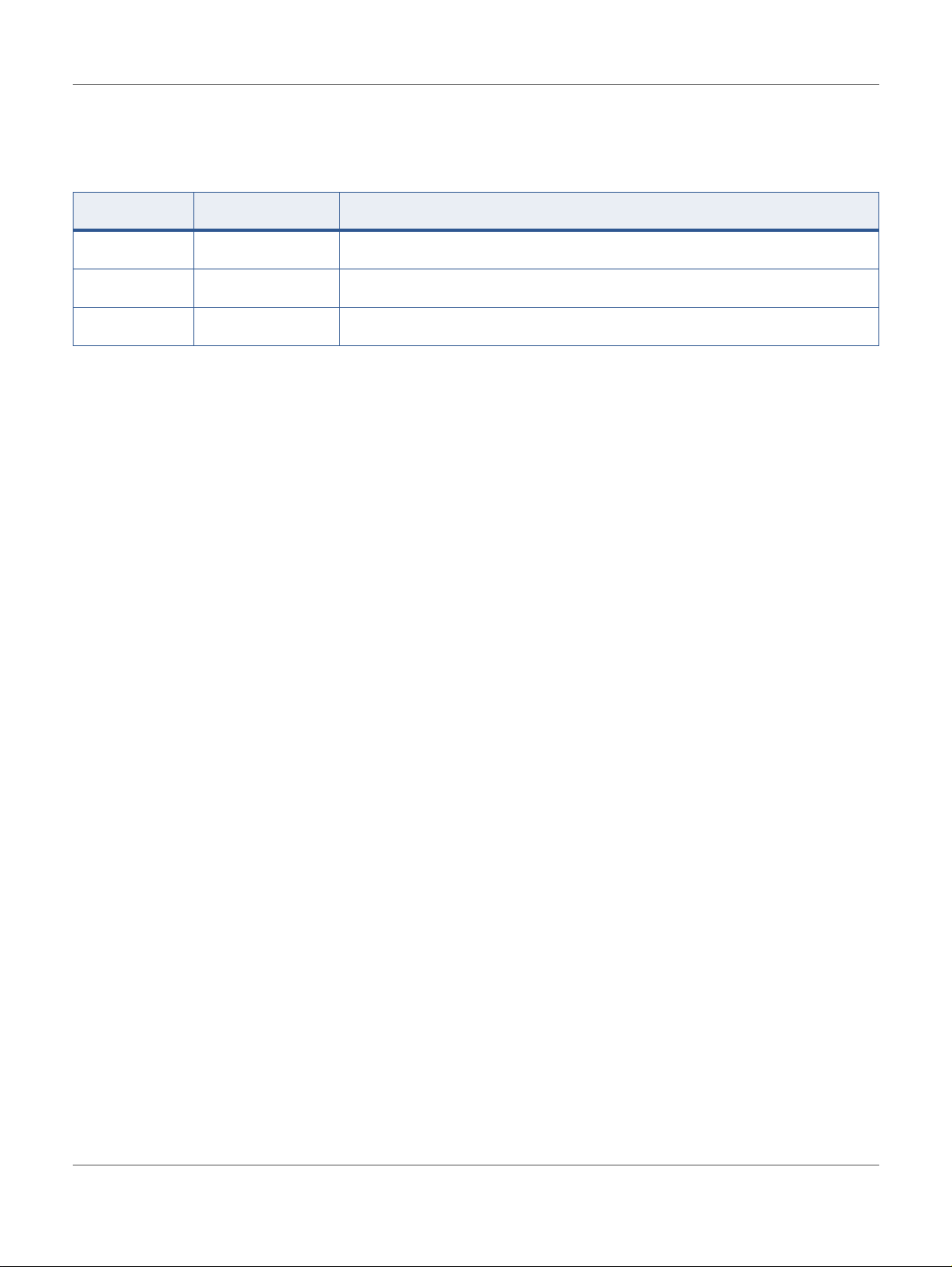
General Conventions
Note Important information requiring the user’s attention.
Caution A condition or circumstance that may cause damage to the equipment or loss of
data.
Warning A condition or circumstance that may cause personal injury.
Italics Italic font style denotes
• emphasis of an important word;
• first use of a new term;
• title of a document.
Screen Name Sans serif, bold font denotes
• on-screen name of a window, dialog box or field;
• keys on a keyboard;
• labels printed on the equipment.
Software Conventions
Code Regular Courier font denotes code or text displayed on-screen.
Code Bold Courier font denotes commands and parameters that you enter exactly as
shown. Multiple parameters are grouped in brackets [ ]. If you are to choose only
one among grouped parameters, the choices are separated with a pipe: [parm1 |
parm2 | parm3] If there is no pipe separator, you must enter each parameter:
[parm1 parm2 parm3]
Code Italic Courier font denotes parameters that require you to enter a value or
variable. Multiple parameters are grouped in brackets [ ]. If you are to choose
only one among grouped parameters, the choices are separated with a pipe:
[parm1 | parm2 | parm3] If there is no pipe separator, you must enter a value for
each parameter: [parm1 parm2 parm3]
SP150Q DATASHEET PROPRIETARY v
SEQUANS Communications

Table of Contents
Preface . . . . . . . . . . . . . . . . . . . . . . . . . . . . . . . . . . . . . . i
Legal Notices . . . . . . . . . . . . . . . . . . . . . . . . . . . . . . . . . . . . . . . . . . . . . . . . . . . . . . . . . . . . . . . . . . . . . . .i
Document Revision History . . . . . . . . . . . . . . . . . . . . . . . . . . . . . . . . . . . . . . . . . . . . . . . . . . . . . . . . . . . ii
About this Datasheet . . . . . . . . . . . . . . . . . . . . . . . . . . . . . . iii
Purpose and Scope . . . . . . . . . . . . . . . . . . . . . . . . . . . . . . . . . . . . . . . . . . . . . . . . . . . . . . . . . . . . . . . . . iii
Who Should Read this Datasheet . . . . . . . . . . . . . . . . . . . . . . . . . . . . . . . . . . . . . . . . . . . . . . . . . . . . . . iii
Changes in this Document . . . . . . . . . . . . . . . . . . . . . . . . . . . . . . . . . . . . . . . . . . . . . . . . . . . . . . . . . . . iii
References . . . . . . . . . . . . . . . . . . . . . . . . . . . . . . . . . . . . . . . . . . . . . . . . . . . . . . . . . . . . . . . . . . . . . . . .iv
Documentation Conventions . . . . . . . . . . . . . . . . . . . . . . . . . . . . . . . . . . . . . . . . . . . . . . . . . . . . . . . . . . v
Chapter 1
Product Features . . . . . . . . . . . . . . . . . . . . . . . . . . . . . . . . . 1
1.1 Features Description . . . . . . . . . . . . . . . . . . . . . . . . . . . . . . . . . . . . . . . . . . . . . . . . . . . . . . 1
1.2 TDM-PCM Interface Specification . . . . . . . . . . . . . . . . . . . . . . . . . . . . . . . . . . . . . . . . . . 5
Chapter 2
Regulatory Approval . . . . . . . . . . . . . . . . . . . . . . . . . . . . . . . 6
Chapter 3
Physical Characteristics . . . . . . . . . . . . . . . . . . . . . . . . . . . . . 9
3.1 ECCN and Part Number . . . . . . . . . . . . . . . . . . . . . . . . . . . . . . . . . . . . . . . . . . . . . . . . . . . 9
3.2 Electrical Operating Conditions . . . . . . . . . . . . . . . . . . . . . . . . . . . . . . . . . . . . . . . . . . . . 10
3.2.1 Detailed Information . . . . . . . . . . . . . . . . . . . . . . . . . . . . . . . . . . . . . . . . . . . . . . . . . 10
3.3 Environmental Operating Conditions . . . . . . . . . . . . . . . . . . . . . . . . . . . . . . . . . . . . . . . . 11
3.3.1 Temperature . . . . . . . . . . . . . . . . . . . . . . . . . . . . . . . . . . . . . . . . . . . . . . . . . . . . . . . 11
3.3.2 Humidity . . . . . . . . . . . . . . . . . . . . . . . . . . . . . . . . . . . . . . . . . . . . . . . . . . . . . . . . . . 11
3.4 Auxiliary ADC Specification . . . . . . . . . . . . . . . . . . . . . . . . . . . . . . . . . . . . . . . . . . . . . . 12
3.5 Power Supply Dimensioning . . . . . . . . . . . . . . . . . . . . . . . . . . . . . . . . . . . . . . . . . . . . . . 12
3.6 I/O Characteristics . . . . . . . . . . . . . . . . . . . . . . . . . . . . . . . . . . . . . . . . . . . . . . . . . . . . . . 13
3.7 Package Description . . . . . . . . . . . . . . . . . . . . . . . . . . . . . . . . . . . . . . . . . . . . . . . . . . . . . 17
3.7.1 Module Footprint . . . . . . . . . . . . . . . . . . . . . . . . . . . . . . . . . . . . . . . . . . . . . . . . . . . 17
3.7.2 Marking Information . . . . . . . . . . . . . . . . . . . . . . . . . . . . . . . . . . . . . . . . . . . . . . . . 20
3.8 Packing Information . . . . . . . . . . . . . . . . . . . . . . . . . . . . . . . . . . . . . . . . . . . . . . . . . . . . . 22
3.9 Storage Conditions . . . . . . . . . . . . . . . . . . . . . . . . . . . . . . . . . . . . . . . . . . . . . . . . . . . . . . 23
3.10 Mounting Considerations . . . . . . . . . . . . . . . . . . . . . . . . . . . . . . . . . . . . . . . . . . . . . . . . . 24
3.11 Component Reliability . . . . . . . . . . . . . . . . . . . . . . . . . . . . . . . . . . . . . . . . . . . . . . . . . . . 25
Proprietary vi
SEQUANS Communications

Table of Contents
3.12 RF Performance . . . . . . . . . . . . . . . . . . . . . . . . . . . . . . . . . . . . . . . . . . . . . . . . . . . . . . . . 27
Chapter 4
Signals and Pins . . . . . . . . . . . . . . . . . . . . . . . . . . . . . . . . 29
4.1 SP150Q Pinout . . . . . . . . . . . . . . . . . . . . . . . . . . . . . . . . . . . . . . . . . . . . . . . . . . . . . . . . . 29
4.2 Notes on SP150Q Signals . . . . . . . . . . . . . . . . . . . . . . . . . . . . . . . . . . . . . . . . . . . . . . . . . 34
4.2.1 High-Speed UARTs Flow Control Signals . . . . . . . . . . . . . . . . . . . . . . . . . . . . . . . 34
4.2.2 I2S/PCM Interface Signals . . . . . . . . . . . . . . . . . . . . . . . . . . . . . . . . . . . . . . . . . . . . 36
4.3 Power Supplies Environment . . . . . . . . . . . . . . . . . . . . . . . . . . . . . . . . . . . . . . . . . . . . . . 37
4.4 Power-up Sequence. . . . . . . . . . . . . . . . . . . . . . . . . . . . . . . . . . . . . . . . . . . . . . . . . . . . . . 37
4.5 Low Power Mode . . . . . . . . . . . . . . . . . . . . . . . . . . . . . . . . . . . . . . . . . . . . . . . . . . . . . . . 39
Appendix A
Acronyms . . . . . . . . . . . . . . . . . . . . . . . . . . . . . . . . . . . . 42
Proprietary vii
SEQUANS Communications
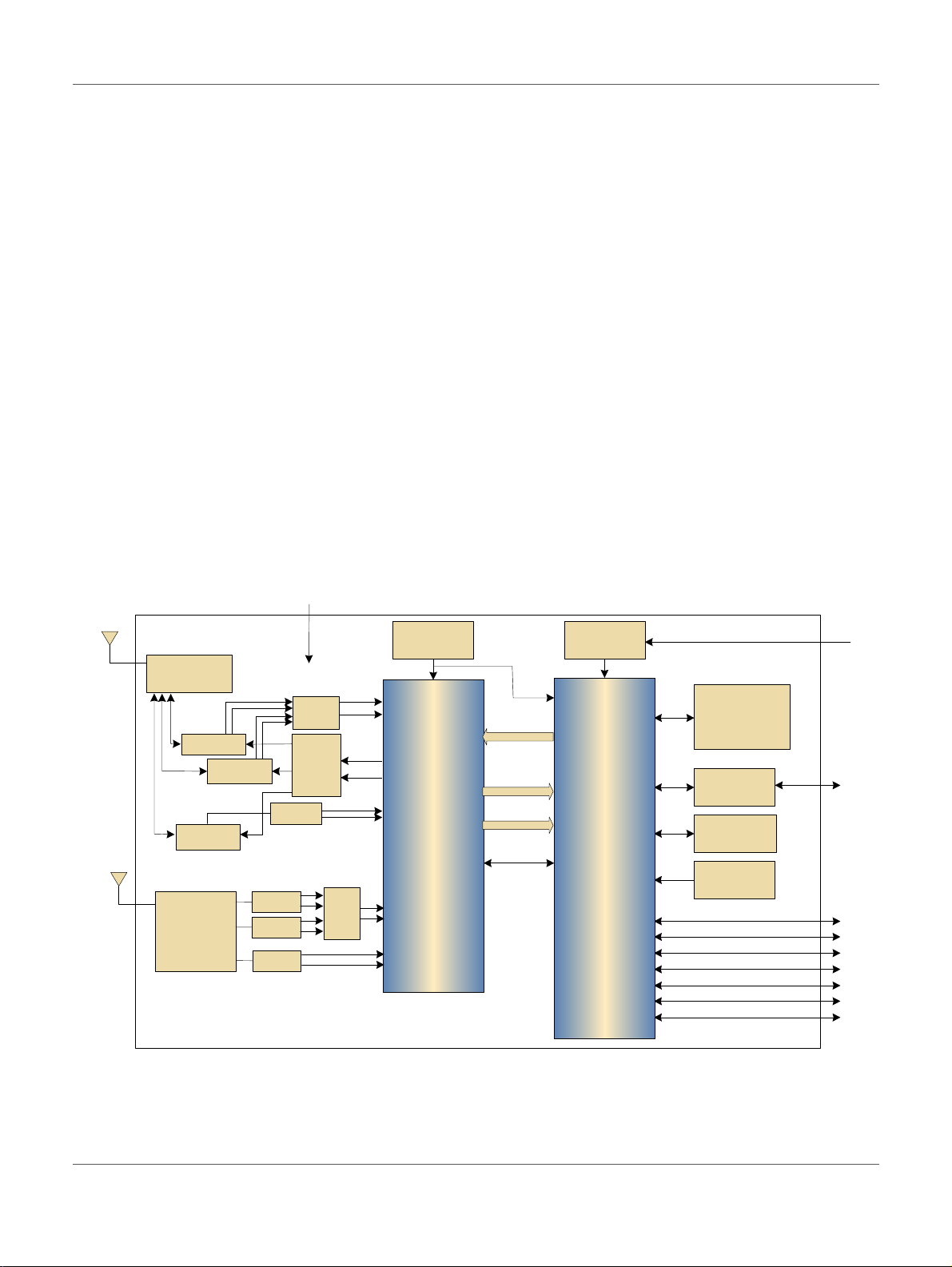
Product Features
^YEϯϮϰϭ
ϱϭϮDďŝƚ>WZ
^W/&ůĂƐŚ
;ϮϱϲDďŝƚͿ
ϯϮϳϲϴŬ,njyƚĂů
WD/dyK
^Wϯd
Z&^ǁŝƚĐŚ
^Wϯd
Z&^ǁŝƚĐŚ
W
WƌŝŵĂƌLJ
ŶƚĞŶŶĂ
ŝǀĞƌƐŝƚLJ
ŶƚĞŶŶĂ
^WϭϱϬY
ϭϮƵƉůĞdžĞƌ
Ϯϲϱ
ƵƉůĞdžĞƌ
hZdƐ
:d'
h^
^/K
WD/Ϯ^
ϭϮ^t
Ϯϲϱ
^t
dy/&
Zy/&Ϭ
Zy/&ϭ
ϯϴϰD,nj
><Z&
sďĂƚ
^/D>ĞǀĞů^ŚŝĨƚĞƌ
^/D
'W/K
^W/
^YEϯϮϮϯ
ŽŶƚƌŽů
sďĂƚ
;ƚŽWƐͿ
ϮϱϮ
^t
ŝĨĨ
ƐǁŝƚĐŚ
ϮϱϮ
ƵƉůĞdžĞƌ
ŝĨĨ
ƐǁŝƚĐŚ
ϮϱĂůƵŶ
1
1.1 Features Description
Sequans SP150Q module includes Calliope Category 1 baseband, a complete
triple band RF front end, memory and required circuitry to meet 3GPP
E-UTRA (Long Term Evolution - LTE, Release 10 set of specifications) and
Sprint LTE UE specifications.
For more information on the core technology specifications see the section
References on page 2. The term SP150Q module refers to the hardware and
the associated embedded software.
The architecture block diagram of the SP150Q is presented on Figure 1-5.
SP150Q DATASHEET PROPRIETARY 1
Figure 1-1: SP150Q Block Diagram
Table 1-1 on page 2 provides detail on general features of the SP150Q.
SEQUANS Communications

Table 1-2 on page 2 provides detail for the LTE-related features of the SP150Q.
SP150Q’s ECCN and part number are detailed in the Section 3.1 ECCN and
Part Number on page 9.
Table 1-1: General Features
PRODUCT FEATURES
FEATURES DESCRIPTION
General interfaces
Supported Frequency Bands
Operation voltages
Packaging
Operating temperature
•JTAG
•USIM
•SPI
•GPIO
• USB 2.0 Host or Device
•UART (x3)
•SDIO Host
•PCM/I2S
•LTE Band 25
•LTE Band 26
•LTE Band 2
•LTE Band 5
•LTE Band 12
•V
(operational range from 3.3 V to 4.42 V)
bat
•LGA module
• 108 pads (22.53 x 22.66 x 1.47 mm)
• RoHS compliant, halogen-free
• -30°C to +60 °C ambient
See also Section 3.3 Environmental Operating Conditions on page 11
Humidity
• 10% to 85%
See also Section 3.3 Environmental Operating Conditions on page 11
Table 1-2: LTE Fea t ur e s
Standard compliance
SP150Q DATASHEET PROPRIETARY 2
• 3GPP E-UTRA Release 10 compliant
SEQUANS Communications

PRODUCT FEATURES
FEATURES DESCRIPTION
Table 1-2: LTE Features (Continued)
PHY
• One UL and two DL transceivers
• Category 1 UE
•FDD
• Normal and extended cyclic prefix
• Modulation
- DL: QPSK, 16QAM, 64QAM
- UL: QPSK, 16QAM
• All coding schemes corresponding to modulations
• All channel coding (turbo-coding with interleaver, tail biting convolutional coding,
block and repetition coding) and CRC lengths
• Channels 5, 10, 15, and 20 MHz
• Sounding (including in special subframes)
• Control and data in special subframes
• Antenna diversity on DL: MRC (Maximum Ratio Combining)
• All power control schemes and DL power allocation schemes
• HARQ Incremental Redundancy and Chase Combining, with bundling or multiplexing
• Measurements and computations related to CQI (Channel Quality Indicator), PMI
(Pre-coding Matrix Indicator) and RI (Rank Indicator), RSRP, and RSRQ
• Low power modes, including Power Gating
MAC
RLC
PDCP
• Random Access procedure in normal and special subframes
• Scheduling Request, Buffer Status Reporting, and Power Headroom Reporting
• Discontinuous reception (DRX) with long and short cycles
• Fast scanning
• Hosted configuration
• Semi-persistent scheduling
•IPv4, IPv6
•RoHC
• Location based services
• Advanced QoS features
• ARQ modes: UM, AM, and TM
• Ciphering and deciphering: NULL, AES, SNOW 3G
• Integrity and protection: AES, SNOW 3G
3 PROPRIETARY SP150Q DATASHEET
SEQUANS Communications

Table 1-2: LTE Features (Continued)
PRODUCT FEATURES
FEATURES DESCRIPTION
RRC
NAS and above
UICC
• MIB and all SIBs
• Intra and inter-frequency measurements and handover
• Up to 8 Data Radio Bearers supported
• MFBI (Multi-Frequency Band Indicator). FGI 35 Enabled
• Frequency Hopping
• Connected Mode Mobility
• PUSCH Hopping
• ANR (Automatic Neighbor Relation)
•NAS
• IMS Client (SMS) or SMS over SG
•OMADM Client
•Pre-loaded APN
• Device supports BIP messaging (all bearers)
• Client Initiated BIP
• LTE IP Messaging
• UICC 312530 IMSI Card Support
• UICC 311882 IoT card support
• Device supports removable UICC
• Device supports ISIM
• Device supports SIM OTA Server initiated polling requests via SMSPP
• Device supports SIM OTA provisioning of user credentials into the UICC from the
SIM OTA server instead of OMA DM
• Device will read APN values from the UICC instead of receiving them from OMA DM
SP150Q DATASHEET PROPRIETARY 4
SEQUANS Communications

PRODUCT FEATURES
TDM-PCM INTERFACE SPECIFICATION
1.2 TDM-PCM Interface Specification
The features of the SP150Q’s TDM-PCM controller include:
• Support of PCM slave mode with PCM_CLK input and PCM_FS input.
• Support of PCM master mode with with PCM_CLK input and PCM_FS
output generated internally
• PCM_CLK input frequency from 128 kHz to 8192 kHz
• Variable number of time-slots within a frame depending on PCM_CLK
frequency
• Support of PCM data format of 8-bits or 16-bits
• In master mode, SP150Q can generate other Frame Sync periods than the
standard Frame Sync period (125 µs).
• Support of short and long Frame Sync formats (active for 1 or 3 PCM_CLK
periods)
• Separated programmable time-slot-offset value for Tx and Rx, for each
voice channel.
It supports two channels of voice over TDM-PCM. This support is provided
by having two complete PCM controllers, each with its own full register set.
These two controllers are time division multiplexed on the PCM bus.
Sequans PCM interface takes PCM_CLK as an input in both master and slave
modes. It supports a set of different frequencies, in the range 128 kHz to 8192
kHz.
Caution: This clock signal is an input in both master and slave modes.
The signals implementing the PCM interface are detailed in 4.2.2 I2S/PCM
Interface Signals on page 36.
5 PROPRIETARY SP150Q DATASHEET
SEQUANS Communications

2
Regulatory Approval
Attention
FCC-ID: 2AAGMSP150Q (limited modular approval)
This above identified LTE radio module is not intended to be provided to
end-users but is for installation by OEM integrators only.
Installation/Integration
OEM integrators must follow Sequans installation instructions to provide for
and benefit from FCC compliant module integrations and must abide
especially by the following:
The maximum antenna gain values (accounting for cable attenuation) to
comply with the FCC maximum ERP/EIRP limits and with RF Exposure rules
will be provided in a future revision of this document for the following bands:
• LTE band 25 (1900+)
• LTE band 26 (850+)
• LTE band 2 (1900 PCS)
• LTE band 5 (850)
• LTE band 12 (700 a)
The Sequans' module integration guidelines must be closely followed.
Compliance of host integrations of the module is limited to hosts adaptation
designs which are identical to Sequans' reference design.
Host integrations with adaption designs deviating from Sequans' reference
design require either class 2 permissive change to this modular approval or a
separate host approval with different FCC-ID;
Host integrations with co-located (simultaneously operating) radio
transmitters must be evaluated in accordance with FCC multi-transmitter
rules and may require either class 2 permissive change to this modular
approval or a separate host approval with different FCC-ID, dependent on the
result of the evaluation; Inquiry at FCC or a TCB is urgently recommended.
Integrations of the module into host products which are intended for portable
use, i.e. less than 20cm distance between its radiating structures (antenna) and
the body of nearby persons, or which otherwise put additional technical
requirements like Hearing Aid compatibility require either class 2 permissive
SP150Q DATASHEET PROPRIETARY 6
SEQUANS Communications

REGULATORY APPROVAL
change to this modular approval or a separate host approval with different
FCC-ID;
Compliance with Unwanted Emission Limits for Digital Device
If the OEM host integration fully complies with the above described reference
design and can completely inherit and rest on compliance of the existing
modular approval the OEM remains still responsible to show compliance of
the overall end-product with the FCC limits for unwanted conducted and
radiated emissions from the digital device (unintentional radio) portion of
such end-product (commonly addressed as part 15B compliance or similar).
End-product Labelling
•FCC-ID
The module's FCC-ID must either be visible from the exterior of the host
product (e.g. per window) or per electronic display, or shall be displayed
on an additional exterior label per the following or similar string:
contains FCC-ID: 2AAGMSP150Q
• Digital Device - Unwanted Emissions Notice
If the end-product falls under part 15 of the FCC rules (it shall display the
following user notice on its exterior acc. to part 15.19 (the notice may be
printed in the manual in case the host is too small):
This device complies with Part 15 of the FCC Rules.Operation is
subject to the following two conditions:
(1) This device may not cause harmful interference,
and
(2) This device must accept any interference received, including
interference that may cause undesired operation.
• Further Labelling Requirements may apply dependent on the FCC rule
parts relevant to the host product.
• End-product User Instructions / Notices in the Manual
At a minimum, end-product users must be provided with the following
notices at a prominent location of the product literature furnished with the
product:
* Product Modifications
Modifications not expressly approved by the party responsible for
compliance could void the user's authority to operate this
equipment.
* RF Exposure Compliance
This equipment complies with FCC radio frequency radiation exposure
rules and limits set forth for an uncontrolled environment, when
installed and operated with minimum distance of 20cm between its
radiating structures (antenna) and the body of nearby persons and
when not operated simultaneously with other nearby
radio-transmitters.
7 PROPRIETARY SP150Q DATASHEET
SEQUANS Communications

REGULATORY APPROVAL
• Maximum Antenna Gain
The user instructions of end-products equipped with standard external
antenna connectors for the modular radio transmitter providing the option
to connect other antennae than those which may or may not be bundled
with the end-product must list the maximum allowed antenna gain values
as derived from those given above, accounting for the cable attenuations of
the actual installation.
• Digital Device - Unwanted Emissions Notice
If the end-product is or contains a digital device (unintentional radio
portions) and is not exempted by its use case (like vehicular use) the
following part 15.105 (b) user notice shall be provided at prominent location of the product literature:
This equipment has been tested and found to comply with the limits
for a Class B digital device, pursuant to part 15 of the FCC rules.
These limits are designed to provide reasonable protection against
harmful interference in a residential installation.
This equipment generates uses and can radiate radio frequency
energy and, if not installed and used in accordance with the
instructions, may cause harmful interference to radio
communications. However, there is no guarantee that interference
will not occur in a particular installation. If this equipment does
cause harmful interference to radio or television reception, which
can be determined by turning the equipment off and on, the user is
encouraged to try to correct the interference by one or more of the
following measures:
o Reorient or relocate the receiving antenna.
o Increase the separation between the equipment and receiver.
o Connect the equipment into an outlet on a circuit different from
that to which the receiver is connected.
o Consult the dealer or an experienced radio/TV technician for help
• Further User Notices
May be required dependent on the FCC rule parts relevant to the host
product.
• Non-allowed User Instructions
The end-product user guidance may NOT include instructions about how
to install or de-install the module.
SP150Q DATASHEET PROPRIETARY 8
SEQUANS Communications

Physical Characteristics
3
3.1 ECCN and Part Number
The ECCN (Export Control Classification Number) of the SP150Q will be
provided in a future revision of this document.
The orderable part number of the SP150Q module is:
• S150R53QRZ for Engineering samples, first revision with RF untested
• S150R53QRA for Engineering samples, second revision
• S150R53QRB for mass production modules compliant with specifications
listed in Section 3.12 RF Performance on page 27
Please contact your Sequans representative to choose the part number that
you should order.
SP150Q DATASHEET PROPRIETARY 9
SEQUANS Communications

PHYSICAL CHARACTERISTICS
ELECTRICAL OPERATING CONDITIONS
3.2 Electrical Operating Conditions
3.2.1 Detailed Information
Table 3-1: Electrical Operating Conditions for SP150Q
Direction Minimum Typical Maximum
VBAT1 In 3.3 V 4.42 V
SIM_VCC (1.8 V or 3.0 V) Out 1.62 V 1.8 V 1.98 V
2.7V 3.0V 3.3V
1V8
See note below.
VCC1_PA In 3.3 V 3.8 V 4.42 V
VCC2_PA In 3.3 V 3.4 V 4.42 V
Out 1.71 V 1.8 V 1.89 V
Note: The maximum current consumption allowed from the 1V8 refer-
ence pin is 50 mA.
Table 3-2: Electrical Maximum Rating for SP150Q
Direction Minimum Typical Maximum
VBAT1 In 3.135 V 5.5 V
VCC1_PA In 3..0 V 3.8 V 5.5 V
VCC2_PA In 0.6 V 3.4 V 5.5 V
SP150Q DATASHEET PROPRIETARY 10
SEQUANS Communications

PHYSICAL CHARACTERISTICS
ENVIRONMENTAL OPERATING CONDITIONS
3.3 Environmental Operating Conditions
3.3.1 Temperature
Note: The temperatures listed here are ambient.
• Operating: -30°C to +60°C
• Storage: -40°C to +85°C
3.3.2 Humidity
• Operating: 10% to 85% (non condensing)
• Storage: 5% to 85% (non condensing)
11 PROPRIETARY SP150Q DATASHEET
SEQUANS Communications

3.4 Auxiliary ADC Specification
Table 3-3: Aux ADC Specification
Performance
Specification
Description
PHYSICAL CHARACTERISTICS
AUXILIARY ADC SPECIFICATION
Value
UnitMinimum Ty pic al Maximum
AUX_ADC
voltage range
AUX_ADC
resolution
AUX_ADC
tolerance
AUX_ADC input
capacitance
AUX_ADC input
resistance
AUX_ADC ENOB including noise and
distortion
AUX_ADC tolerance after calibration. Please
contact Sequans’ technical support for details
on AUX_ADC calibration.
AUX_ADC input capacitance
Note: Spec is valid in all conditions whether
AUX_ADC used or not, also includes SHUT
mode with 3V supply removed
AUX_ADC input resistance
Note: Spec is valid in all conditions whether
AUX_ADC used or not, also includes SHUT
mode with 3V supply removed
02V
10 bit
-2 +2 %
10 kOhm
3.5 Power Supply Dimensioning
2pF
Note: Information useful for power supply module dimensionning will
be provided in a future revision of this document. Note also that
average and detailed power consumption figures are provided in
Sequans’ Software Release Notes.
SP150Q DATASHEET PROPRIETARY 12
SEQUANS Communications

PHYSICAL CHARACTERISTICS
I/O CHARACTERISTICS
3.6 I/O Characteristics
The voltage and current characteristics of the various IO pads of the SP150Q
versus IO bank supply voltage are illustrated in the tables below.
Caution: Note that the Voh values in the tables below do not apply to
GPIOs configured in open drain mode. GPIOs can be individually
configured in open drain mode. When in open drain mode they
either drive the line to V
an external pull-up resistance. The PCB designer must ensure that
the voltage on these pads never exceeds Vih of the IO group to
which they belong.
Table 3-4 details the various pad types as listed in SP150Q signals list.
Table 3-4: Pad Types Detail
Pad Type Description
, or leave it floating, to be pulled up by
ol
Maximum
Input High Voltage
analog analog (or power for powers and ground for grounds) Not Applicable
BIDIR_DDR 1.8 V in/out. Refer to Table 3-6 for DC IO characteristics. V
BIDIR_PD 1.8 V in/out with software controlled internal pull-down.
Refer to Table 3-5 for DC IO characteristics.
BIDIR_PD_SLEW_SCHMITT 1.8 V slew-rate controlled in/out with Schmitt trigger and
software controlled internal pull-down.Refer to Table 3-5
for DC IO characteristics.
BIDIR_PU 1.8 V in/out with software controlled internal
pull-up.Refer to Table 3-5 for DC IO characteristics.
IN 1.8V input. V
IN_PD 1.8 V input with software controlled internal
pull-down.Refer to Table 3-5 for DC IO characteristics.
IN_PU 1.8V input with software controlled internal pull-up. V
OUT 1.8 V output.Refer to Ta ble 3 -5 for DC IO characteristics. V
max = 1.9 V
IH
max = 3.6 V
V
IH
max = 3.6 V
V
IH
max = 3.6 V
V
IH
max = 3.6 V
IH
max = 3.6 V
V
IH
max = 3.6 V
IH
max = 3.6 V
IH
Refer to SP150Q Pin List to know the type of IO pad used on every
termination.
• The Minimum values for I
and Ioh should not be exceeded to guarantee
ol
that the logical level are not spoiled for each pad type.
• The Nominal values for I
and Ioh represent the nominal values for the pad
ol
type. They are provided for information only.
13 PROPRIETARY SP150Q DATASHEET
SEQUANS Communications

•The Maximum values for Iol and Ioh represent the maximal values for the
pad type. They are provided for information only.
Table 3-5: DC Characteristics for Digital IOs, Voltage 1.8 V
Parameter Drive Strength Min. Nom. Max. Unit
PHYSICAL CHARACTERISTICS
I/O CHARACTERISTICS
V
IL
Input Low Voltage
V
IH
Input High Voltage
V
T
Threshold Point
V
T+
Schmitt Trigger Low to High Threshold Point
V
T-
Schmitt Trigger High to Low Threshold Point
V
T PU
Threshold Point with Pull-up Resistor Enabled
V
T PD
Threshold Point with Pull-down Resistor Enabled
V
T+ PU
Schmitt Trigger Low to High Threshold Point with Pull-up Resistor Enabled
-0.3 0.63 V
1.17 3.6 V
0.79 0.87 0.94 V
1 1.12 1.22 V
0.61 0.71 0.8 V
0.79 0.86 0.93 V
0.8 0.87 0.95 V
1 1.12 1.21 V
V
T- PU
0.61 0.7 0.8 V
Schmitt Trigger High to Low Threshold Point with Pull-up Resistor Enabled
V
T+ PD
1.01 1.13 1.23 V
Schmitt Trigger Low to High Threshold Point with Pull-down Resistor Enabled
V
T- PD
0.62 0.72 0.81 V
Schmitt Trigger High to Low Threshold Point with Pull-down Resistor Enabled
I
I
±10 µA
Input Leakage Current @ VI=1.8V or 0V
I
OZ
±10 µA
Tri-state Output Leakage Current @ VO=1.8V or 0V
Input Capacitance 3 pF
R
PU
56 89 148 kOhm
Pull-up Resistor
SP150Q DATASHEET PROPRIETARY 14
SEQUANS Communications

PHYSICAL CHARACTERISTICS
I/O CHARACTERISTICS
Table 3-5: DC Characteristics for Digital IOs, Voltage 1.8 V (Continued)
Parameter Drive Strength Min. Nom. Max. Unit
R
PD
Pull-down Resistor
V
OL
Output Low Voltage
V
OH
Output High Voltage
I
OL
Low Level Output Current at VOL(max)
I
OH
High Level Output Current at VOH(max)
52 90 167 kOhm
0.45 V
1.35 V
2 mA 1.2 2.2 3.6 mA
4 mA 2.3 4.3 7.1 mA
8 mA 4.6 8.6 14.3 mA
2 mA 1.0 2.4 4.6 mA
4 mA 2.0 4.7 9.2 mA
8 mA 4.0 9.4 18.4 mA
Table 3-6: DC Characteristics for Digital IOs, Voltage 1.8 V - DDR IO Pins (BIDIR_DDR
Type)
Parameter Drive Strength Min. Nom. Max. Unit
VDDQ
MOBILE DDR 1.8V I/O power
Input Capacitance 2.689 pF
V
IL
Input Low Voltage
V
IH
Input High Voltage
V
ILD(AC)
AC Input Low Voltage
V
IHD(AC)
AC Input High Voltage
V
OL
Output Low Voltage (IOH=-0.1mA)
1.7 1.8 1.9 V
-0.3 0.3 * VDDQ V
0.7 * VDDQ VDDQ + 0.3 V
-0.3 0.2 * VDDQ V
0.8 * VDDQ VDDQ + 0.3 V
0.1 * VDDQ V
15 PROPRIETARY SP150Q DATASHEET
SEQUANS Communications

PHYSICAL CHARACTERISTICS
I/O CHARACTERISTICS
Table 3-6: DC Characteristics for Digital IOs, Voltage 1.8 V - DDR IO Pins (BIDIR_DDR
Type) (Continued)
Parameter Drive Strength Min. Nom. Max. Unit
V
OH
0.9 * VDDQ V
Output High Voltage (IOH=-0.1mA)
I
OL
2 mA 2.00 mA
Low Level Output Current at VOL(max)
4 mA 4.00 mA
8 mA 8.00 mA
10 mA 10.00 mA
I
OH
2 mA 2.00 mA
High Level Output Current at VOH(max)
4 mA 4.00 mA
8 mA 8.00 mA
10 mA 10.00 mA
Table 3-7: DC Characteristics for MODULE_PWR_EN, Voltage VDD_PWR_EN
Parameter Drive Strength Min. Nom. Max. Unit
V
IL
Input Low Voltage
V
IH
Input High Voltage
-0.3 0.4 V
1.1 VBAT1 + 0.3 V
SP150Q DATASHEET PROPRIETARY 16
SEQUANS Communications

PHYSICAL CHARACTERISTICS
PACKAGE DESCRIPTION
3.7 Package Description
3.7.1 Module Footprint
The dimensions marked in Figure 3-1are listed in Table 3-8.
Figure 3-1: Top and Side View of the SP150Q
Table 3-8: SP150Q Outline Dimensions
Mark Minimum (mm) Nominal (mm) Maximum (mm)
A 22.43 22.53 22.63
B 22.56 22.66 22.76
C Not available 1.47 1.55
D Not available Not available 0.08
17 PROPRIETARY SP150Q DATASHEET
SEQUANS Communications

PHYSICAL CHARACTERISTICS
PACKAGE DESCRIPTION
Figure 3-2: Bottom Side View of the SP150Q Pads
Attention: T1 to T30 pads are used as both GND and thermal drops.
Table 3-9: SP150Q Dimensions and Tolerances
Mark Dimension and tolerance (mm)
L 22.53 ± 0.1
W 22.66 ± 0.1
A1 12 ± 1.0
A2 4.125 ± 0.5
A3 10.8 ± 1.0
A4 4.725 ± 0.5
A5 0.6 ± 0.05
SP150Q DATASHEET PROPRIETARY 18
SEQUANS Communications

PHYSICAL CHARACTERISTICS
PACKAGE DESCRIPTION
Table 3-9: SP150Q Dimensions and Tolerances (Continued)
Mark Dimension and tolerance (mm)
A6 1.2 ± 0.1
A7 0.6 ± 0.05
B1 0.9 ± 0.1
B2 0.325 ± 0.05
B3 0.6 ± 0.05
B4 19.2 ± 0.2
B5 18 ± 0.2
B6 1.075 ± 0.1
B7 1.675 ± 0.15
C1 6.125 ± 0.5
C2 6.8 ± 0.5
C3 1.2 ± 0.01
C4 0.5 ± 0.05
D1 0.5 ± 0.05
D2 0.9 ± 0.1
D3 7 ± 0.5
D4 6.725 ± 0.5
D5 18.9 ± 0.2
D6 15.9 ± 0.2
19 PROPRIETARY SP150Q DATASHEET
SEQUANS Communications

3.7.2 Marking Information
Note: The marking information can be either laser marking or high
temperature label.
PHYSICAL CHARACTERISTICS
PACKAGE DESCRIPTION
Figure 3-3: SP150Q Marking Description
Table 3-10: Marking Details
Symbol Description
aSequans’ logo
bRoHS logo
c S/N 2D barcode
d Model: SP150Q
e IMEI: 2D barcode
f Calliope logo
gFCC ID: Will be provided in a future revision of this document.
h IMEI :XXXXXXXXXXXXXXX (15 digits)
SP150Q DATASHEET PROPRIETARY 20
SEQUANS Communications

PHYSICAL CHARACTERISTICS
PACKAGE DESCRIPTION
Table 3-10: Marking Details (Continued)
Symbol Description
i S/N: SPAYYMMDDNNNNSSS (16 digits)
SPA: is immovable (3 digits)
YYMMDD: Manufacturing Date (YY:Year, MM:Month, DD:Day)
NNNN: panel counter (from0001~9999)
SSS: Piece location on panel (from001~020)
jMade in PRC
21 PROPRIETARY SP150Q DATASHEET
SEQUANS Communications

3.8 Packing Information
The SP150Q is delivered in Tape-and-Reel. One reel can hold up to 1000 (one
thousand) pieces. Each reel is included in a box, and a carton can contain three
boxes. This is represented on Figure 3-4.
PHYSICAL CHARACTERISTICS
PACKING INFORMATION
Figure 3-4: SP150Q Packing Description
SP150Q DATASHEET PROPRIETARY 22
SEQUANS Communications

PHYSICAL CHARACTERISTICS
STORAGE CONDITIONS
3.9 Storage Conditions
1. Calculated shelf life in sealed bag : 12 months at < 40°C and < 90% RH.
2. After the moisture barrier bag (MBB) is opened, devices that will be
subjected to reflow solder or other high temperature process must be:
a) mounted within 168 hours under factory conditions = 30°C/60%RH, or
b) Stored as per J-STD-033.
3. Devices require dry bake, before mounting, if
a) Humidity Indicator Card reads >10% for level 2a-5a devices or >60% for
level 2 devices when read at 23±5°C
b) 2a or 2b conditions above are not met.
4. If dry bake is required, refer to IPC/JEDEC J-STD-033 for bake procedure.
Note: Level and body temperature are defined by IPC/JEDEC
J-STD-020.
23 PROPRIETARY SP150Q DATASHEET
SEQUANS Communications

3.10 Mounting Considerations
This section provides reflow information.
Figure 3-5: Reflow Profile
PHYSICAL CHARACTERISTICS
MOUNTING CONSIDERATIONS
The SP150Q can support up to 3 reflows with 250°C maximum.
Table 3-11: Reflow Parameters
Parameter Setting
Peak package body temperature Will be provided in a future revision of the document.
Liquidous Time
Preheat/Soak
Ramp-up rate
Ramp-down rate
SP150Q DATASHEET PROPRIETARY 24
SEQUANS Communications

PHYSICAL CHARACTERISTICS
COMPONENT RELIABILITY
3.11 Component Reliability
Table 3-12: SP150Q Reliability Figures
Test Ite m Test M e thod Tes t Co n d itions Test Result
ESD - Direct Discharge
(ANT GND)
ESD Direct Discharge HBM MIL-STD-883J / Method
Half-Sine Shock Test Step1: Module 15pcs,
Vibration Test Sweep-Sine Vibration
IEC 61000-4-2 M.2 board. See detail
inTable 3-13 below.
3015.8
MM ANSI/ESD S5.2-2009 ±50V to ±200V with 50V
CDM JESD22-C101F NCDM Start: ±500V, Stop:
drop height 30cm, drop
direction 26 drops (all
surfaces, edges and
corners)
Step2: M2 Card 20pcs,
500G, 1.0msec, 6drops
(6 faces, 1drop/face
and Random Vibration
PASS. See details inTab le
3-14 and Table 3 - 1 5
below.
±500V to ±2000V with
500V steps
steps
±500V
PAS S
PAS S
Bump Test Half Sine, 250m/s2, 6ms,
2bumps/s, 1000bumps
per ±axis
Low Temperature
Storage test
High Temperature
Storage test
25 PROPRIETARY SP150Q DATASHEET
SEQUANS Communications
-40°C, 500 hours PASS
85°C, 500 hours PASS
PAS S
Table 3-13: SP150Q ESD Test Conditions (IEC 61000-4-2 Standard)
Test Parame t e r Description
Discharge Voltage Direct Discharge Air 8 kV
Contact 4 kV
Indirect Discharge HCP 4 kV
VCP 4 kV
Polarity Positive / Negative
Discharge Impedance 330 Ohm
Discharge Capacitance 150 pF
Number of Discharge Minimum 10 times at all test point for Air condition.
Minimum 25 times at all test point for Contact condition.
Minimum 25 times at all test point for HCP/VCP condition.
PHYSICAL CHARACTERISTICS
COMPONENT RELIABILITY
Discharge Mode 1 time per second
Table 3-14: Description of Criterium of ESD Test
Criterion Description
A The equipment shall continue to operate as intended without operator intervention. No degradation
of performance or loss of function is allowed below a performance level specified by the
manufacturer when the equipment is used as intended. The performance level may be replaced by a
permissible loss of performance. If the minimum performance level or the permissible performance
loss is not specified by the manufacturer, then either of these may be derived from the product
description and documentation, and by what the user may reasonably expect from the equipment if
used as intended.
Table 3-15: ESD (Indirect Discharge) Test Results
Test Level (kV) Polarity (+/-) Te st Point HCP Result VCP Result
4 kV +/- 4 sides A A
SP150Q DATASHEET PROPRIETARY 26
SEQUANS Communications

PHYSICAL CHARACTERISTICS
RF PERFORMANCE
3.12 RF Performance
This section presents the module’s performance in LTE Band 25, Band 26,
Band 2, Band 5 and Band 12.
Note: The values presented in Table 3-16 and Table 3-17 are currently
estimated performance results. They will be updated with
measures done on parts S150R53QRB.
Note: UE complies with 3GPP 36.521-1 Table 6.2.2.5-1: UE Power Class
test requirements, including 0.7 dB for measurement errors.
Table 3-16: Uplink
LTE Band Number Low Freq (MHz) High Freq (MHz) EARFCN
Typical
Output Power
(dBm)
B25 1850 1915 Will be provided in a
future revision of the
B26 814 849 +23.5
B2 1850 1910 +23.0
B5 824 849 +23.5
B12 699 716 +23.5
document
+23.0
Table 3-17: Downlink
LTE Band Number Low Freq (MHz) High Freq (MHz) EARFCN
B25 1930 1995 Will be provided in a
future revision of the
B26 859 894 -103
B2 1930 1990 -101
B5 869 894 -103
document
-101
Sensitivity
5 MHz (dBm)
B12 729 746 -103
27 PROPRIETARY SP150Q DATASHEET
SEQUANS Communications

PHYSICAL CHARACTERISTICS
RF PERFORMANCE
The results for the typical sensitivity levels are measured under the following
test conditions:
• 2 receive paths
• Tx power @ 23 dBm. UL allocation: 20RB, offset 5 for Band 12, and full allocation for Band 25/2 and Band 26/5.
SP150Q DATASHEET PROPRIETARY 28
SEQUANS Communications

Signals and Pins
4
4.1 SP150Q Pinout
Table 4-1 lists the function and main information for SP150Q pads.
The pads listed in Table 4-2 are connected to ground.
Refer also to Figure 4-1 that represents the typical implementation for UART
hardware flow control.
Table 4-1: Pinout
Pad
#
2 NETWORK_LED GPO_3,
3 1V8 Out Reference voltage for IOs.
4 USB_EXT_VBUS_VLD WAKE_2 In
5 FFF_FFH GPIO_18 In - Pull-up for a system boot in FFF mode.
6 ACTIVITY_LED GPO_2 Out
7 MODULE_ON_IND GPIO_19 Out Module “ON” Indicator.
8 HWID1 GPIO_27 In This signal shall be pull-up.
9 DNC/HSIC_DATA In/Out Reserved, do not connect.
10 HWID2 GPIO_28 In This signal shall be pull-up.
Pad Name
Alternate
Function
SPI_CS_N_2
Direction
(HW)
Out
Comments
Note: it can be used to provide power small devices
(50 mA max usage)
- Pull-down for a system boot in FFH mode.
11 DNC/HSIC_STROBE Out Reserved, do not connect.
12 SIM_RSTN Out
13 USB_D+ In/Out
SP150Q DATASHEET PROPRIETARY 29
SEQUANS Communications

Table 4-1: Pinout (Continued)
SIGNALS AND PINS
SP150Q PINOUT
Pad
#
Pad Name
Alternate
Function
Direction
(HW)
Comments
14 SIM_CLK Out
15 USB_D- In/Out
16 SIM_DETECT In SIM_DETECT = 1 signals that a card is present.
SIM_DETECT = 0 signals that no card is present.
17 SIM_IO In/Out
18 SIM_VCC Out
19 SDIO_HOST_D2 GPO_6 In / Out
21 SDIO_HOST_CLK GPO_9 Out
23 SDIO_HOST_CMD GPO_8 In/Out
25 SDIO_HOST_D1 GPO_5,
In / Out
WA KE _ 3
27 SDIO_HOST_D0 GPO_4 In / Out
29 SDIO_HOST_D3 GPO_7 In / Out
35 PCM_RXD GPIO_10 In PCM receive data. See details in Section 4.2.2
I2S/PCM Interface Signals on page 36.
36 PCM_CLK GPO_1 In PCM clock input, from 128 kHz to 8192 kHz. See
details in Section 4.2.2 I2S/PCM Interface Signals on
page 36.
37 PCM_FS GPIO_9 In/Out Frame synchronization at 8 kHz. See details in
Section 4.2.2 I2S/PCM Interface Signals on page 36.
38 PCM_TXD GPIO_8 Out PCM transmit data. See details in Section 4.2.2
I2S/PCM Interface Signals on page 36.
39 RFDATA_12 Out
40 RFDATA_18 Out
41 RFDATA_19 Out
44 ANT1 In Auxiliary antenna
47 RESET_N In
48 JTAG_TDO Out
SP150Q DATASHEET PROPRIETARY 30
SEQUANS Communications

SIGNALS AND PINS
SP150Q PINOUT
Table 4-1: Pinout (Continued)
Pad
#
Pad Name
Alternate
Function
Direction
(HW)
Comments
49 JTAG_TRSTN In
50 JTAG_TMS In
51 JTAG_TDI In
52 JTAG_TCK In
54 ANT0 In / Out Main antenna
56 UART0_SOUT GPIO_35 Out
57 AUX_ADC In
58 UART0_SIN GPIO_34 In
59 SPI_SDI GPIO_44 Out Data from SP150Q module to SPI device.
60 SPI_CS_N_1 GPIO_47 Out
61 SPI_CLK GPIO_43 Out
67 SPI_SDO GPIO_45 In Data from SPI device to SP150Q module.
75 UART2_CTS GPIO_6 In UART2 flow control, Clear-To-Send, active low, of
the SP150Q. See details in Section 4.2.1 High-Speed
UARTs Flow Control Signals on page 34.
76 UART2_RTS GPIO_7 Out UART2 flow control, Ready-To-Send, active low, of
the SP150Q. See details in Section 4.2.1 High-Speed
UARTs Flow Control Signals on page 34.
77 UART2_SIN GPIO_4 In
78 UART3_SIN GPIO_14 In
79 UART2_SOUT GPIO_5 Out
80 UART3_SOUT GPIO_15 Out
81 UART3_RTS GPIO_17 Out UART3 flow control, Ready-To-Send, active low, of
the SP150Q. See details in Section 4.2.1 High-Speed
UARTs Flow Control Signals on page 34.
82 SQN3223_GPIO_38 In / Out
31 PROPRIETARY SP150Q DATASHEET
SEQUANS Communications

Table 4-1: Pinout (Continued)
SIGNALS AND PINS
SP150Q PINOUT
Pad
#
Pad Name
Alternate
Function
Direction
(HW)
Comments
83 UART3_CTS GPIO_16 In UART3 flow control, Clear-To-Send, active low, of
the SP150Q. See details in Section 4.2.1 High-Speed
UARTs Flow Control Signals on page 34.
84 SQN3223_GPIO_41 In / Out
85 SQN3223_GPIO_39 In / Out
88 SQN3223_GPIO_24 In / Out
89 SQN3223_GPIO_25 In / Out
90 SQN3223_GPIO_40 In / Out
91 SQN3223_GPIO_26 In / Out
92 SQN3223_GPIO_20 In / Out
93 SQN3223_GPIO_23 In / Out
94 SQN3223_GPIO_22 In / Out
95 SQN3223_GPIO_21 In / Out
96 WAKE_1 GPIO_3 In
97 VCC1_PA In
98 VCC2_PA In
99 VCC2_PA In
100 DNC Do Not Connect, reserved
101 DNC Do Not Connect, reserved
102 DNC Do Not Connect, reserved
103 DNC Do Not Connect, reserved
104 WAKE_0 In See details in Section 4.5 Low Power Mode on page
39.
105 SAR_DETECT GPIO_42 In / Out
106 MODULE_PWR_EN In See IO Characteristics for VDD_PWR_EN
107 VBAT1 In
SP150Q DATASHEET PROPRIETARY 32
SEQUANS Communications

SIGNALS AND PINS
SP150Q PINOUT
Table 4-1: Pinout (Continued)
Pad
#
Pad Name
Alternate
Function
108 VBAT1 In
Table 4-2: Ground Pads
Pad # Pad Name Comment
1
20 22 24 26 28
30 31 32 33 34
42 43 45 46
53 55
62 63 64 65 66 68 69
70 71 72 73 74
86 87
T1 T2 T3 T4 T5 T6 T7 T8 T9 T10
T11 T12 T13 T14 T15 T16 T17 T18 T19 T20
T21 T22 T23 T24 T25 T26 T27 T28 T29 T30
Direction
(HW)
Comments
GND All GND pads shall be connected to the same
copper.
GND All GND pads shall be connected to the same
copper.
33 PROPRIETARY SP150Q DATASHEET
SEQUANS Communications

NOTES ON SP150Q SIGNALS
4.2 Notes on SP150Q Signals
4.2.1 High-Speed UARTs Flow Control Signals
• UART2_CTS: UART2 flow control, Clear-To-Send, active low, of the
SP150Q. To be connected to the RTS of the remote UART device. Provision
a 1 kOhm pull-down on CTS pin when flowcontrol is not used. If it is
connected to an external component (like a RS232 driver), the user should
make sure that this component will present a low level to the SP150Q. See
Figure 4-1.
• UART2_RTS: UART2 flow control, Ready-To-Send, active low, of the
SP150Q. To be connected to the CTS of the remote UART device. See Figure
4-1.
• UART3_CTS: UART3 flow control, Clear-To-Send, active low, of the
SP150Q. To be connected to the RTS of the remote UART device. Provision
a 1 kOhm pull-down on CTS pin when flowcontrol is not used. If it is
connected to an external component (like a RS232 driver), the user should
make sure that this component will present a low level to the SP150Q.
Figure 4-1.
SIGNALS AND PINS
• UART3_RTS: UART3 flow control, Ready-To-Send, active low, of the
SP150Q. To be connected to the CTS of the remote UART device. See Figure
4-1.
SP150Q DATASHEET PROPRIETARY 34
SEQUANS Communications

SIGNALS AND PINS
'E 'E
^/E
^Khd
Zd^
d^
'E
Zy
dy
Zd^
d^
'E
^ĞƋƵĂŶƐ^/ ZĞŵŽƚĞĞǀŝĐĞ
NOTES ON SP150Q SIGNALS
Figure 4-1 represents the typical implementation for the hardware
flowcontrol.
Figure 4-1: UART Flow Control
Note: High-Speed UART can be used as low-speed UART, given a
specific software registers configuration and the setting of the
CTS signal to 0. Please contact Sequans customer support for
details.
35 PROPRIETARY SP150Q DATASHEET
SEQUANS Communications

4.2.2 I2S/PCM Interface Signals
• PCM_RXD: PCM receive data. PCM data block is 8-bits or 16-bits. Only one
data block is received per frame. Receive time-slot offset is programmable
by using the RX_SLOT register. For instance, if RX_SLOT=5, then the 8-bit
data block is received from time-slot #5 to #12. Bit-order is configurable.
• PCM_CLK: PCM clock input, from 128 kHz to 8192 kHz
Sequans PCM interface takes PCM_CLK as an input in both master and
slave modes.
Caution: This clock signal is an input in both master and slave modes.
When choosing a clock source for PCM_CLK, it is important to ensure that
the selected frequency is supported by the IC connected to SP150Q's PCM
interface.
The choice of frequency depends on:
– Sampling frequency Fs
– Number of bits per sample Nbps
– Number of slots per PCM frame
SIGNALS AND PINS
NOTES ON SP150Q SIGNALS
It is given by the following formula:
PCM_CLK = Fs * Nbps * slots-per-PCM-frame
Where SP150Q supports:
– All commonly used sampling frequencies (8 kHz, 16 kHz, 32 kHz, 44.1
kHz, 48 kHz, 96 kHz, 192 kHz, 22.05 kHz, 44.1 kHz, 88.2 kHz, 176.4
kHz)
– 8 or 16 bits per sample (Nbps)
– 1 to (1024/Nbps) slots per PCM frame
• PCM_FS: Frame synchronization at 8 kHz. The number of time-slots within
a frame varies, depending on PCM_CLK frequency. To be flexible in offset
configuration, we define one PCM clock period per time-slot. Therefore, in
8-bit format, 8 time-slots are used to receive or transmit one 8-bit data
block. If PCM_CLK=128 kHz, there are 16 time-slots per frame. If
PCM_CLK=8192 kHz, there are 1024 time-slots per frame. In master mode,
PCM_FS is an output generated internally. In slave mode, PCM_FS is an
input. Both short and long Frame Sync standards are supported. Short
Frame Sync is high for one and only one PCM clock period. Long Frame
Sync is high for three consecutive PCM clock periods. In both cases, the
positive edge of PCM_FS occurs every 125 µs.
• PCM_TXD: PCM transmit data. PCM data block is 8-bits or 16-bits. Only
one data block is transmitted per frame. Transmit time-slot offset is
programmable by using the TX_SLOT register. For instance, if TX_SLOT=8,
then the 8-bit data block is transmitted from time-slot #8 to #15. Bit-order is
configurable. PCM_TXD is in low-impedance during data transmission,
otherwise it is in high impedance.
SP150Q DATASHEET PROPRIETARY 36
SEQUANS Communications

SIGNALS AND PINS
WD/
W
sd
sdϭ
sϮͺW
sϭͺW
^WϭϱϬYW
ƚƐϭ
ƚƐ
ŽůĚƐƚĂƌƚ
sdϭ
DKh>ͺWtZͺE
Z^dͺE
POWER SUPPLIES ENVIRONMENT
4.3 Power Supplies Environment
Figure 4-3 illustrates the connections between the power supplies of the
SP150Q.
Figure 4-2: SP150Q Power Supplies Diagram
4.4 Power-up Sequence
Note: After each module boot, the modem will issue +SYSSTART URC.
The following timing requirement applies to the signals VBAT1,
MODULE_PWR_EN and RESET_N. It must be respected for proper SP150Q’s
behavior.
Caution: VBAT1 and VBAT2 should remain stable in the voltage range
listed in Table 3-2; if this condition is not met, the internal OTP
(One-Time Programmable) area of the baseband chip might be
randomly corrupted and it can lead to a non-functional and unrecoverable state preventing the module to correctly boot.
Figure 4-3: VBAT1, MODULE_PWR_EN and RESET_N Signals Timing
Requirement for Cold Start
37 PROPRIETARY SP150Q DATASHEET
SEQUANS Communications

SIGNALS AND PINS
ƚƐϭ
tĂƌŵƐƚĂƌƚ
Z^dͺE
sdϭ
DKh>ͺWtZͺE
ƚŚϭ
ZĞƐĞƚĐLJĐůĞ
sdϭ
DKh>ͺWtZͺE
Z^dͺE
POWER-UP SEQUENCE
Figure 4-4: VBAT1, MODULE_PWR_EN and RESET_N Signals Timing
Requirement for Warm Start
Figure 4-5: VBAT1, MODULE_PWR_EN and RESET_N Signals Timing
Requirement for Reset Cycle
The timing minimum values are listed in Table 4-3 .
Table 4-3: VBAT1, MODULE_PWR_EN and RESET_N Signal Timing Values
Symbol Description Minimum Duration Maximum Duration
ts VBAT1 setup time 0 ms -
ts1 RESET_N setup time 1 ms -
th1 RESET_N hold time 1 µs -
SP150Q DATASHEET PROPRIETARY 38
SEQUANS Communications

SIGNALS AND PINS
LOW POWER MODE
4.5 Low Power Mode
The SP150Q integrates several mechanisms to support power consumption
optimization during operation and during low-power mode.
SP150Q can be woken from low power mode through:
• USB resume signaling (when the host supports it)
• USB plug / unplug event (reported by the signal USB_EXT_VBUSVLD)
• SDIO interrupt on SDIO_HOST_D1
• Two dedicated input signal WAKE_0 and WAKE_1
Note: Wake from activity on the UARTx interfaces is not possible
directly. It can be achieved by connecting a SP150Q's GPIO
driven by the external device before resuming UARTx
activity.
In a use case where a device on the far end of a UART link needs
to wake SP150Q, that device must provide a signal to one of
SP150Q's WAKE_x signals.
If the end device has an output that says it is ready to transmit a
character over the UART, then that signal can be connected to one
of the SP150Q's WAKE_x signals. If not, then that device should
use a GPIO or other signal to stimulate SP150Q's WAKE_x signal.
WAKE_x signals are active only when the SP150Q is asleep.
To get the lowest possible power consumption during low-power mode, all
IOs must be stable. At software configuration time, take care of the following,
to prevent them from being in conflict or floating:
• Pads that are not driven by an external device shall be driven low by software if they have a GPIO or GPO or RFDATA mode that allows it.
• For pads that are known to be driven by an external device:
Configure that external device to hold the signal stable during low-power
mode, and configure SP150Q to treat that pin as an input, without internal
pull-up or pull-down.
• For pads where, at the time of low-power mode, the signal may or may not
be driven by an external device:
Configure SP150Q to enable the internal pull-up/pull-down on the pad to
guarantee that it will not be floating during low-power mode.
39 PROPRIETARY SP150Q DATASHEET
SEQUANS Communications

SIGNALS AND PINS
LOW POWER MODE
The signals involved in the low-power mode of the SP150Q are listed in Ta ble
4-4.
Note: Each signal’s pull (up or down) is determined by register. It can
be modified by software.
Table 4-4: Signals Related to Low-Power Mode
Signal Name Drive Description
SDIO_HOST_D1 Open-drain Possible wakeup by SDIO Host activity.
See important note below.
USB_EXT_VBUSVLD Open-drain Possible wakeup by USB activity. USB_EXT_VBUSVLD is
driven low and indicates USB cable presence if value is 1
(based on VBUS).
See important note below.
WA KE _0
Input with pull-down
1
Default setting is to wake on high to low transition.
Available for user application.
The software can configure SP150Q to wake from low power
mode when this signal is high, or when this signal is low.
Alternatively, software can configure SP150Q to ignore this
signal when it is in low power mode.
See important notes below.
WAKE_1 Input Default setting is to wake on high to low transition.
Available for user application.
The software can configure SP150Q to wake from low power
mode when this signal is high, or when this signal is low.
Alternatively, software can configure SP150Q to ignore this
signal when it is in low power mode.
See important note below.
1. Internal pull-down resistor has 30 kOhm to 72 kOhm value.
SP150Q DATASHEET PROPRIETARY 40
SEQUANS Communications

SIGNALS AND PINS
LOW POWER MODE
Important Notes
1. SDIO_HOST_D1
This signal is muxed with WAKE_3, which is transition configurable. To
trigger an interrupt, the designer must map WAKE_3 signal to a dedicated
GPIO. The pulse on GPIO must be long enough (typically 8 ms) to be
detected in any mode.
This feature might not be activated in the software release preloaded in the
module. Please contact Sequans technical support if you intend to use it.
2. USB_EXT_VBUSVLD
This signal is muxed with WAKE_2, which is transition configurable. To
trigger an interrupt, the designer must map WAKE_2 signal to a dedicated
GPIO. The pulse on GPIO must be long enough (typically 8 ms) to be
detected in any mode.
This feature might not be activated in the software release preloaded in the
module. Please contact Sequans technical support if you intend to use it.
3. WAKE_0
a) As default software configuration, WAKE_0 detects a low level to
wake-up the baseband; this behavior can be changed by software. To
trigger an interrupt, the designer must map WAKE_0 signal to a dedicated GPIO. The pulse on GPIO must be long enough (typically 8 ms)
to be detected in any mode. Please refer to Module Integration Guide
or Sequans Technical Support for more detail.
b) Extra current leakage occurs when WAKE_0 is high and the module in
low power mode. It is then recommended to introduce a tiny logic
inverter gate in front of WAKE_0 when WAKE_0 is high in low-power
mode; you can also consider to use WAKE_1 if possible. The extra
current leakage does not occur when WAKE_0 is low when the module
is in low power mode (wake on level high).
4. WAKE_1
As default software configuration, WAKE_1 detects a low level to wake-up
the baseband; this behavior can be changed by software.
This feature might not be activated in the software release preloaded in the
module. Please contact Sequans technical support if you intend to use it.
41 PROPRIETARY SP150Q DATASHEET
SEQUANS Communications

Acronyms
A
Acronym Definition
ADC Analog to Digital Converter
CPU Central Processing Unit
DL Downlink
ECCN Export Control Classification Number
ECM Ethernet Control Model, USB interface
EEM Ethernet Emulation Model, USB interface
ENOB Effective number of bits
ESD Electro-static discharge
ETSI European Telecommunications Standard Institute
FFF Firmware from Flash. Specific load and boot mode for the module.
FFH Firmware from Host. Specific load and boot mode for the module.
GND Ground
GNSS Global Navigation Satellite System
GPIO General Purpose Input Output
HBM Human Body Model (ESD)
HCP Horizontal Coupling Plane
I/O Input/Output
I2C Inter-Integrated Circuit interface
IMEI International Mobile Equipment Identity
SP150Q DATASHEET PROPRIETARY 42
SEQUANS Communications

Acronym Definition
IMS Instant Messaging Service
IP Internet Protocol
JTAG Joint Test Action Group
LGA Large Grid Array
LTE Long Term Evolution, or 4G. Standard is developed by the 3GPP
www.3gpp.org.
MIMO Multiple In Multiple Out
MM Machine Model (ESD)
NAS Network Access Server
OMADM Open Mobile Alliance Device Management
PCM Pulse-Code Modulation
PHY Physical Layer
QTY Quantity
RB Resource Block
RF Radio Frequency
RoHS Restriction of Hazardous Substances
Rx Reception
S/N or SN: Serial Number
SDM Socketed Device Model (ESD)
SIM Subscriber Identification Module
SMS Short Message Service
SPI Serial Peripheral Interface
SPI Serial Peripheral Interface
Tx Transmission
UART Universal Asynchronous Receiver Transmitter
UE User Equipment
43 PROPRIETARY SP150Q DATASHEET
SEQUANS Communications

Acronym Definition
UL Uplink
USB Universal Serial Bus
VCP Vertical Coupling Plane
SP150Q DATASHEET PROPRIETARY 44
SEQUANS Communications
 Loading...