


Monarch Platform - GM01Q Module
SEQUANS Communications
15-55 Boulevard Charles de Gaulle
92700 Colombes, France
Phone. +33.1.70.72.16.00
Fax. +33.1.70.72.16.09
www.sequans.com
contact@sequans.com
Datasheet

Legal Notices
Copyright ©2017-2018, SEQUANS Communications
All information contained herein and disclosed by this document is
confidential and the proprietary property of SEQUANS Communications,
and all rights therein are expressly reserved. Acceptance of this material
signifies agreement by the recipient that the information contained in this
document is confidential and that it will be used solely for the purposes set
forth herein. Acceptance of this material signifies agreement by the recipient
that it will not be used, reproduced in whole or in part, disclosed, distributed,
or conveyed to others in any manner or by any means – graphic, electronic, or
mechanical, including photocopying, recording, taping, or information
storage and retrieval systems – without the express written permission of
SEQUANS Communications.
Preface
All Sequans’ logos and trademarks are the property of SEQUANS
Communications. Unauthorized usage is strictly prohibited without the
express written permission of SEQUANS Communications. All other
company and product names may be trademarks or registered trademarks of
their respective owners. Products and services of SEQUANS
Communications, and those of its licensees may be protected by one or more
pending or issued U.S. or foreign patents.
Because of continuing developments and improvements in design,
manufacturing, and deployment, material in this document is subject to
change without notification and does not represent any commitment or
obligation on the part of SEQUANS Communications. SEQUANS
Communications shall have no liability for any error or damages resulting
from the use of this document.
GM01Q DATASHEET PROPRIETARY i
SEQUANS Communications

Document Revision History
Revision Date Product Application
05 August 2018 Fifth edition of the document.
06 September 2018 Sixth edition of the document.
07 November 2018 Seventh edition of the document. See list of changes in Section Changes
in this Document on page iii.
ii PROPRIETARY GM01Q DATASHEET
SEQUANS Communications

About this Datasheet
Purpose and Scope
The GM01Q is a complete certified LTE Category M1 module including
base-band, RF and memory, for the design of connected machine-to-machine
devices, and other Internet-of-Things devices with embedded LTE
connectivity. This document provides technical information about GM01Q
LGA module. GM01Q is based on Sequans’ Monarch platform.
Who Should Read this Datasheet
This document is intended for engineers who are developing User Equipment
(UE) for LTE systems.
Changes in this Document
The changes since the previous edition of the document are as follows:
• Updated FCC statement in Section Regulatory Approval on page 4.
• Updated Section 3.1 ECCN and Part Number on page 7 and updated part
numbers in the document.
• Added module weight in Section 3.9 Package Description on page 17.
• Added MSL3 compliancy is Section 3.11 Storage Conditions on page 21.
GM01Q DATASHEET PROPRIETARY iii
SEQUANS Communications

References
[1] Core technology specifications:
• 3GPP E-UTRA 21 series Release 13 (EPS)
• 3GPP E-UTRA 22 series Release 13 (IMEI)
• 3GPP E-UTRA 23 series Release 13 (NAS, SMS)
• 3GPP E-UTRA 24 series Release 13 (NAS)
• 3GPP E-UTRA 31 series Release 13 (UICC)
• 3GPP E-UTRA 33 series Release 13 (security)
• 3GPP E-UTRA 36 series Release 13 (RAN)
• 3GPP2 C.S0015-A v1.0 (SMS)
• IETF, RFC 3261, 4861, 4862, 6434
For more information, see
• ftp://ftp.3gpp.org/Specs/archive/
• http://www.3gpp2.org/public_html/specs/CS0015-0.pdf
• https://tools.ietf.org/html/
[2] Test specifications:
3GPP E-UTRA 36 series Release 13 (RAN)
ftp://ftp.3gpp.org/Specs/archive/
[3] Vocabulary reference:
• 3GPP TR 21.905: "Vocabulary for 3GPP Specifications"
For more information, see http://www.3gpp.org/ftp/specs/archive/21_series/21.905/
iv PROPRIETARY GM01Q DATASHEET
SEQUANS Communications
Documentation Conventions
This section illustrates the conventions that are used in this document.
General Conventions
Note Important information requiring the user’s attention.
Caution A condition or circumstance that may cause damage to the equipment or loss of
data.
Warning A condition or circumstance that may cause personal injury.
Italics Italic font style denotes
• emphasis of an important word;
• first use of a new term;
• title of a document.
Screen Name Sans serif, bold font denotes
• on-screen name of a window, dialog box or field;
• keys on a keyboard;
• labels printed on the equipment.
Software Conventions
Code Regular Courier font denotes code or text displayed on-screen.
Code Bold Courier font denotes commands and parameters that you enter exactly as
shown. Multiple parameters are grouped in brackets [ ]. If you are to choose only
one among grouped parameters, the choices are separated with a pipe: [parm1 |
parm2 | parm3] If there is no pipe separator, you must enter each parameter:
[parm1 parm2 parm3]
Code Italic Courier font denotes parameters that require you to enter a value or
variable. Multiple parameters are grouped in brackets [ ]. If you are to choose
only one among grouped parameters, the choices are separated with a pipe:
[parm1 | parm2 | parm3] If there is no pipe separator, you must enter a value for
each parameter: [parm1 parm2 parm3]
GM01Q DATASHEET PROPRIETARY v
SEQUANS Communications

Table of Contents
Preface . . . . . . . . . . . . . . . . . . . . . . . . . . . . . . . . . . . . . . i
Legal Notices . . . . . . . . . . . . . . . . . . . . . . . . . . . . . . . . . . . . . . . . . . . . . . . . . . . . . . . . . . . . . . . . . . . . . . .i
Document Revision History . . . . . . . . . . . . . . . . . . . . . . . . . . . . . . . . . . . . . . . . . . . . . . . . . . . . . . . . . . . ii
About this Datasheet . . . . . . . . . . . . . . . . . . . . . . . . . . . . . . iii
Purpose and Scope . . . . . . . . . . . . . . . . . . . . . . . . . . . . . . . . . . . . . . . . . . . . . . . . . . . . . . . . . . . . . . . . . iii
Who Should Read this Datasheet . . . . . . . . . . . . . . . . . . . . . . . . . . . . . . . . . . . . . . . . . . . . . . . . . . . . . . iii
Changes in this Document . . . . . . . . . . . . . . . . . . . . . . . . . . . . . . . . . . . . . . . . . . . . . . . . . . . . . . . . . . . iii
References . . . . . . . . . . . . . . . . . . . . . . . . . . . . . . . . . . . . . . . . . . . . . . . . . . . . . . . . . . . . . . . . . . . . . . . .iv
Documentation Conventions . . . . . . . . . . . . . . . . . . . . . . . . . . . . . . . . . . . . . . . . . . . . . . . . . . . . . . . . . . v
Chapter 1
Product Features . . . . . . . . . . . . . . . . . . . . . . . . . . . . . . . . . 1
1.1 Features Description . . . . . . . . . . . . . . . . . . . . . . . . . . . . . . . . . . . . . . . . . . . . . . . . . . . . . . 1
Chapter 2
Regulatory Approval . . . . . . . . . . . . . . . . . . . . . . . . . . . . . . . 4
Chapter 3
Physical Characteristics . . . . . . . . . . . . . . . . . . . . . . . . . . . . . 7
3.1 ECCN and Part Number . . . . . . . . . . . . . . . . . . . . . . . . . . . . . . . . . . . . . . . . . . . . . . . . . . . 7
3.2 Electrical Operating Conditions . . . . . . . . . . . . . . . . . . . . . . . . . . . . . . . . . . . . . . . . . . . . . 8
3.2.1 Detailed Information . . . . . . . . . . . . . . . . . . . . . . . . . . . . . . . . . . . . . . . . . . . . . . . . . . 8
3.2.2 GM01Q Power Tree . . . . . . . . . . . . . . . . . . . . . . . . . . . . . . . . . . . . . . . . . . . . . . . . . . 9
3.2.3 Power Supplies Environment . . . . . . . . . . . . . . . . . . . . . . . . . . . . . . . . . . . . . . . . . . 10
3.3 Environmental Operating Conditions . . . . . . . . . . . . . . . . . . . . . . . . . . . . . . . . . . . . . . . . 10
3.3.1 Temperature . . . . . . . . . . . . . . . . . . . . . . . . . . . . . . . . . . . . . . . . . . . . . . . . . . . . . . . 10
3.3.2 Humidity . . . . . . . . . . . . . . . . . . . . . . . . . . . . . . . . . . . . . . . . . . . . . . . . . . . . . . . . . . 10
3.4 Power Supply Dimensioning . . . . . . . . . . . . . . . . . . . . . . . . . . . . . . . . . . . . . . . . . . . . . . 11
3.5 I/O Characteristics . . . . . . . . . . . . . . . . . . . . . . . . . . . . . . . . . . . . . . . . . . . . . . . . . . . . . . 12
3.6 Auxiliary ADC . . . . . . . . . . . . . . . . . . . . . . . . . . . . . . . . . . . . . . . . . . . . . . . . . . . . . . . . . 15
3.7 Performance . . . . . . . . . . . . . . . . . . . . . . . . . . . . . . . . . . . . . . . . . . . . . . . . . . . . . . . . . . . 16
3.8 Component Reliability . . . . . . . . . . . . . . . . . . . . . . . . . . . . . . . . . . . . . . . . . . . . . . . . . . . 16
3.9 Package Description . . . . . . . . . . . . . . . . . . . . . . . . . . . . . . . . . . . . . . . . . . . . . . . . . . . . . 17
3.9.1 Module Footprint . . . . . . . . . . . . . . . . . . . . . . . . . . . . . . . . . . . . . . . . . . . . . . . . . . . 17
3.9.2 Marking Information . . . . . . . . . . . . . . . . . . . . . . . . . . . . . . . . . . . . . . . . . . . . . . . . 19
3.10 Packing Information . . . . . . . . . . . . . . . . . . . . . . . . . . . . . . . . . . . . . . . . . . . . . . . . . . . . . 20
3.11 Storage Conditions . . . . . . . . . . . . . . . . . . . . . . . . . . . . . . . . . . . . . . . . . . . . . . . . . . . . . . 21
Proprietary vi
SEQUANS Communications

Table of Contents
3.12 Mounting Considerations . . . . . . . . . . . . . . . . . . . . . . . . . . . . . . . . . . . . . . . . . . . . . . . . . 22
Chapter 4
Signal and Pins . . . . . . . . . . . . . . . . . . . . . . . . . . . . . . . . . 23
4.1 GM01Q Pinout . . . . . . . . . . . . . . . . . . . . . . . . . . . . . . . . . . . . . . . . . . . . . . . . . . . . . . . . . 23
4.2 UART Interfaces. . . . . . . . . . . . . . . . . . . . . . . . . . . . . . . . . . . . . . . . . . . . . . . . . . . . . . . . 24
4.3 Power-up Sequence. . . . . . . . . . . . . . . . . . . . . . . . . . . . . . . . . . . . . . . . . . . . . . . . . . . . . . 25
4.4 LTE Low Power Mode . . . . . . . . . . . . . . . . . . . . . . . . . . . . . . . . . . . . . . . . . . . . . . . . . . . 26
4.4.1 General Information . . . . . . . . . . . . . . . . . . . . . . . . . . . . . . . . . . . . . . . . . . . . . . . . . 26
4.4.2 Detailed Behavior of IO Pads of BIDIR Type . . . . . . . . . . . . . . . . . . . . . . . . . . . . . 27
4.4.3 Detailed Behavior of IO Pads of BIDIR_WAKE Type . . . . . . . . . . . . . . . . . . . . . . 28
Appendix A
Acronyms . . . . . . . . . . . . . . . . . . . . . . . . . . . . . . . . . . . . 31
Proprietary vii
SEQUANS Communications
Product Features
'DϬϭY
^YEϯϯϯϬ
&ƌŽŶƚͲŶĚDŽĚƵůĞ
ĂůƵŶ
ĂůƵŶ
>d
ŶƚĞŶŶĂ
sϭͺW
sϮͺW
sdϭ
sϭͺW
sϮͺW
ZydžEE
ZydžEW
ZydžEE
ZydžEW
Z&/
Ɖ^ZD WDh
ϯϮϳϲϴŬ,njyƚĂů
^W/&ůĂƐŚ
;ϭϮϴDďŝƚͿ
dyK
ϯϴϰD,nj
W^ͺ^ddh^
:d'
Z/E'Ϭ
^/D
hZdϬ
hZdϭ
hZdϮ
t<ϭ
t<Ϭ
1
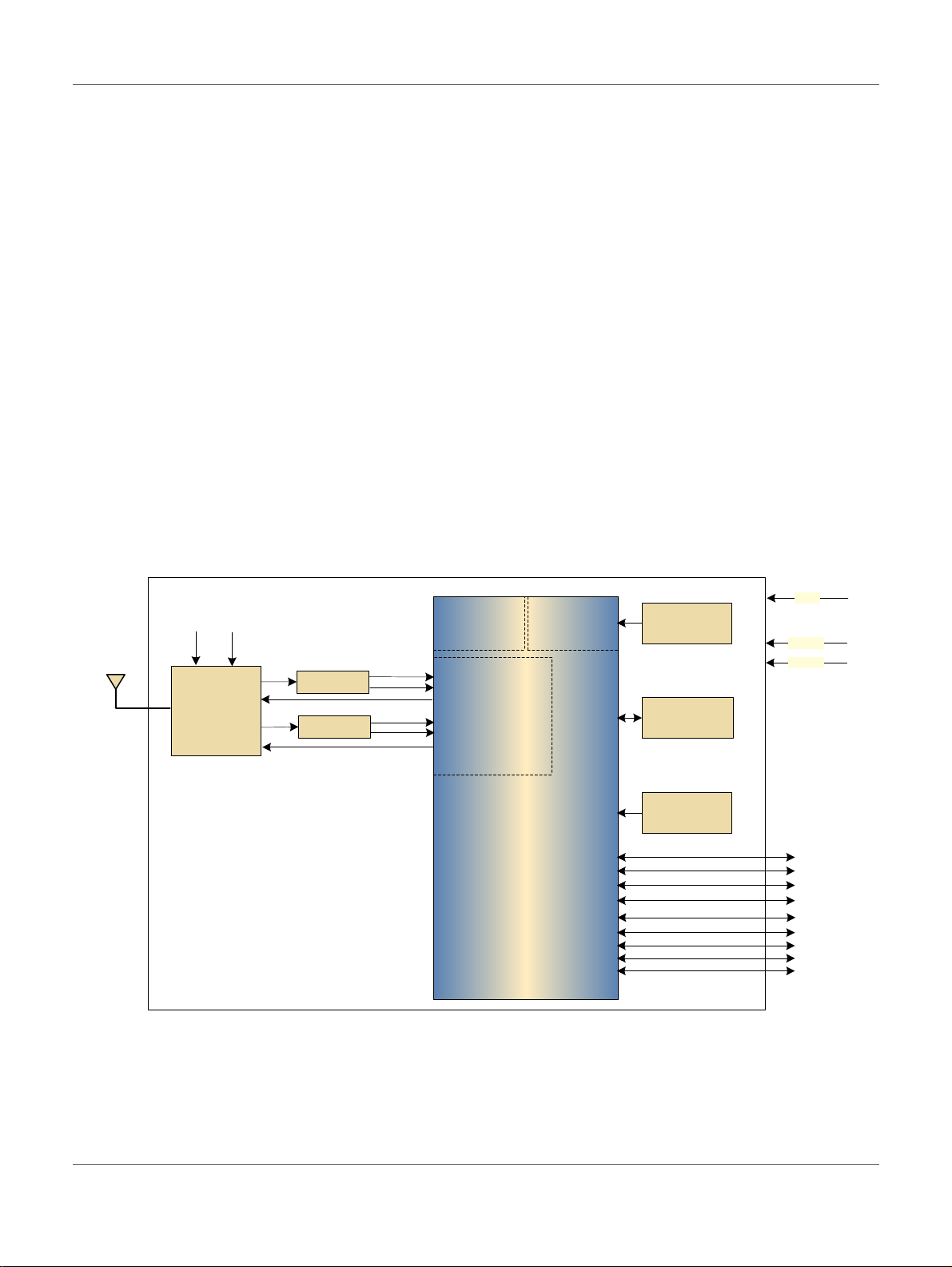
1.1 Features Description
Sequans GM01Q module includes Monarch SQN3330 Cat-M1 baseband, a
complete dual band RF front end, memory and required circuitry to meet
3GPP E-UTRA (Long Term Evolution - LTE, Release 13) Cat-M1 UE
specifications.
For more information on the core technology specifications see the section
References on page iv. The term GM01Q module refers to the hardware and
the associated embedded software.
Figure 1-1: GM01Q Block Diagram
Table 1-1 on page 2 provides detail on general features of the GM01Q.
Table 1-2 on page 2 provides detail for the LTE-related features of the GM01Q.
GM01Q DATASHEET PROPRIETARY 1
SEQUANS Communications

GM01Q’s ECCN and part number are detailed in the Section 3.1 ECCN and
Part Number on page 7.
Table 1-1: General Features
PRODUCT FEATURES
FEATURES DESCRIPTION
General interfaces
•JTAG
• I2C (reserved)
•USIM
• SPI (reserved)
•GPIO
• UART (x3, including one reserved)
Supported Frequency Bands One of the following LTE Bands sets:
• GM01R63QR5 : LTE bands B2, B4, B12
• GM01R63QR6 : LTE bands B3, B28
• GM01R63QR7 : LTE bands B1, B2, B3, B4, B5, B8, B12, B13, B14, B17, B18, B19,
B20, B25, B26, B28, B66
Operation voltages
Packaging
•V
•LGA module
(range from 3.1 V to 4.5 V)
bat1
• 108 pads (21.35 x 20.25 x 1.79 mm)
• RoHS compliant, halogen-free
Operating temperature
• RF compliant -30°C to +60°C (ambient)
• Operational: -40°C to +85°C (board)
See also Section 3.3 Environmental Operating Conditions on page 10.
Humidity
Table 1-2: LTE Fea t ur e s
Standard compliance
• 3GPP E-UTRA Release 13 compliant
• 10% to 85%
See also Section 3.3 Environmental Operating Conditions on page 10.
GM01Q DATASHEET PROPRIETARY 2
SEQUANS Communications

PRODUCT FEATURES
FEATURES DESCRIPTION
Table 1-2: LTE Features (Continued)
PHY
MAC
• One UL and one DL transceiver
• Support of HD-FDD Duplexing
• Channel 1.4 MHz bandwidth
• Normal and extended cyclic prefix
• Support of MPDCCH
• Modulation
- DL: QPSK, 16QAM
- UL: QPSK, 16QAM
• All coding schemes corresponding to modulations
• All channel coding (turbo-coding with interleaver, tail biting convolutional coding,
block and repetition coding) and CRC lengths
• Sounding (including in special subframes)
• Control and data in special subframes
• All power control schemes and DL power allocation schemes
• HARQ Incremental Redundancy and Chase Combining, with bundling or multiplexing
• Measurements and computations related to CQI (Channel Quality Indicator), PMI
(Pre-coding Matrix Indicator) and RI (Rank Indicator), RSRP, and RSRQ
• UEPCOP (from 3GPP Release 12) Power Saving Mode
• Random Access procedure in normal and special subframes
• Scheduling Request, Buffer Status Reporting, and Power Headroom Reporting
• Discontinuous reception (DRX, eDRX) with long and short cycles
• Fast scanning
• Hosted configuration
•IPv4, IPv6
•RoHC
• Location based services
• Advanced QoS features
RLC
PDCP
• ARQ modes: UM, AM, and TM
• Ciphering and deciphering: NULL, AES, SNOW 3G
• Integrity and protection: AES, SNOW 3G
RRC
• MIB and new SIB1bis
• Intra and inter-frequency measurements and handover
• Up to 8 Data Radio Bearers supported
• Support of CE (Coverage Extension) Mode
NAS and above
•NAS
•SMS over SG
• LWM2M Client
3 PROPRIETARY GM01Q DATASHEET
SEQUANS Communications

2
Regulatory Approval
Note:
Attention
GM01R63QR5 FCC-ID: 2AAGMGM01Q (single modular approval)
GM01R63QR7 FCC-ID: 2AAGMGM01QA (single modular approval)
above identified LTE radio module is not intended to be provided to
This
end-users but is for installation by OEM integrators only.
Installation/Integration
OEM integrators must follow Sequans installation instructions to provide for and benefit from
FCC compliant module integrations and must abide especially by the following:
The only FCC-compliant LTE bands are : band 2, band 4, band 12 and band 13.
The maximum antenna gain values (accounting for cable attenuation) to comply with the FCC
maximum ERP/EIRP limits and with RF Exposure rules:
• LTE band 2 (1800 MHz): 2.1 dBi
• LTE band 4 (1700 MHz): 2 dBi
• LTE band 12 (700 MHz): -2 dBi
• LTE band 13 (780 MHz): -2.4 dBi
The Sequans' module integration guidelines must be closely followed.
Compliance of host integrations of the module is limited to hosts adaptation
designs which are identical to Sequans' reference design.
This section applies to GM01R63QR5 and GM01R63QR7 part numbers.
Host integrations with adaption designs deviating from Sequans' reference
design require either class 2 permissive change to this modular approval or a
separate host approval with different FCC-ID;
Host integrations with co-located (simultaneously operating) radio
transmitters must be evaluated in accordance with FCC multi-transmitter
rules and may require either class 2 permissive change to this modular
approval or a separate host approval with different FCC-ID, dependent on the
result of the evaluation; Inquiry at FCC or a TCB is urgently recommended.
Integrations of the module into host products which are intended for portable
use, i.e. less than 20cm distance between its radiating structures (antenna) and
the body of nearby persons, or which otherwise put additional technical
requirements like Hearing Aid compatibility require either class 2 permissive
change to this modular approval or a separate host approval with different
FCC-ID;
GM01Q DATASHEET PROPRIETARY 4
SEQUANS Communications

REGULATORY APPROVAL
Compliance with Unwanted Emission Limits for Digital Device
If the OEM host integration fully complies with the above described reference
design and can completely inherit and rest on compliance of the existing
modular approval the OEM remains still responsible to show compliance of
the overall end-product with the FCC limits for unwanted conducted and
radiated emissions from the digital device (unintentional radio) portion of
such end-product (commonly addressed as part 15B compliance or similar).
End-product Labelling
•FCC-ID
The module's FCC-ID must either be visible from the exterior of the
product
on
(e.g. per window) or per electronic
an additional exterior label per the following or similar string:
display, or shall be displayed
host
contains FCC-ID: 2AAGMGM01Q
• Digital Device - Unwanted Emissions Notice
If the end-product falls under part 15 of the FCC rules (it
following user
printed
in the manual in case the host is too small):
This device complies with Part 15 of the FCC Rules.Operation is
subject to the following two conditions:
(1) This device may not cause harmful interference,
and
(2) This device must accept any interference received, including
interference that may cause undesired operation.
notice on its exterior acc. to part
15.19 (the notice may be
shall display the
• Further Labelling Requirements may apply dependent on the FCC rule
parts relevant
to the host product.
• End-product User Instructions / Notices in the Manual
At a minimum, end-product users must be provided with the following
notices at a prominent location of the product literature furnished with the
product:
* Product Modifications
Modifications not expressly approved by the party responsible for
compliance could void the user's authority to operate this
equipment.
* RF Exposure Compliance
This equipment complies with FCC radio frequency radiation exposure
rules and limits set forth for an uncontrolled environment, when
installed and operated with minimum distance of 20cm between its
radiating structures (antenna) and the body of nearby persons and
when not operated simultaneously with other nearby
radio-transmitters.
• Maximum Antenna Gain
The user instructions of end-produc
ntenna connectors for the modular radio transmitter providing the
a
connect other antennae than those which may or may not be bundle
to
with
the end-product must list the maximum allowed antenna gain values
as derived from those given above, accounting for the cable attenuations
the actual inst
5 PROPRIETARY GM01Q DATASHEET
allation.
SEQUANS Communications
ts equipped with standard external
option
d
of

• Digital Device - Unwanted Emissions Notice
REGULATORY APPROVAL
If the end-product is or contains a digital device (unintention
ions) and is not exempted by its use case (like vehicular use) th
port
following pa
rt 15.105 (b) user notice shall be provided at prominent loca-
al radio
tion of the product literature:
This equipment has been tested and found to comply with the limits
for a Class B digital device, pursuant to part 15 of the FCC rules.
These limits are designed to provide reasonable protection against
harmful interference in a residential installation.
This equipment generates uses and can radiate radio frequency
energy and, if not installed and used in accordance with the
instructions, may cause harmful interference to radio
communications. However, there is no guarantee that interference
will not occur in a particular installation. If this equipment does
cause harmful interference to radio or television reception, which
can be determined by turning the equipment off and on, the user is
encouraged to try to correct the interference by one or more of the
following measures:
o Reorient or relocate the receiving antenna.
o Increase the separation between the equipment and receiver.
o Connect the equipment into an outlet on a circuit different from
that to which the receiver is connected.
o Consult the dealer or an experienced radio/TV technician for help
• Further User Notices
May be required dependent on the FCC rule parts relevant to
the host
product.
e
Non-allowed User Instructions
•
The end-product user guidance may NOT incl
to
install or de-install the module.
ude instructions about how
GM01Q DATASHEET PROPRIETARY 6
SEQUANS Communications

Physical Characteristics
3
3.1 ECCN and Part Number
The orderable part numbers of the GM01Q module are as follows, according
to the supported LTE bands.
• GM01R63QR5 for mass production modules: LTE Bands 2, 4, 12
• GM01R63QR6 for mass production modules: LTE Bands 3, 28
• GM01R63QR7 for engineering samples: LTE Bands 1, 2, 3, 4, 5, 8, 12, 13, 14,
17, 18, 19, 20, 25, 26, 28, 66
Table 3-1 lists the FEM implemented in the module circuitry for each
orderable part number.
Table 3-1: Front-End Module Type per Orderable Part Number
Orderable Part Number PA implemented in the Module
GM01R63QR5 Skyworks® SKY68001
GM01R63QR6 Skyworks® SKY68001
GM01R63QR7 Skyworks® SKY68020
The ECCN of the GM01Q module is 5A992.c. CCATS number is G175554.
The following comment from licensing officer is reported on the license
information:
• This encryption item is described in paragraph B to note 3 (mass market
note) of category 5 part 2. It is authorized for export and reexport under
section 740.17(B)(3) of the export administration regulations (EAR).
GM01Q DATASHEET PROPRIETARY 7
SEQUANS Communications

PHYSICAL CHARACTERISTICS
ELECTRICAL OPERATING CONDITIONS
3.2 Electrical Operating Conditions
3.2.1 Detailed Information
Table 3-2 describes the electrical operating conditions for GM01Q.
Table 3-2: Electrical Operating Conditions
Direction Minimum Typical Maximum
VBAT1 In 3.1 V 4.5 V
SIM_VCC (1.8 V or 3.0 V) Out 1.62 V 1.8 V 1.98 V
2.7V 3.0V 3.3V
1V8
See notes below.
3V0
See note 2 below.
VCC1_PA In 2.85 V 3.0 V 3.3 V
VCC2_PA In 2.85 V 3.0 V 3.3 V
Out 1.71 V 1.8 V 1.89 V
Out 2.85 V 3.0 V 3.15 V
Note:
1. The maximum current consumption allowed from the 1V8
reference pin is 100 mA.
2. Each output reference voltage (1V8, 3V0) can be either
running or powered off depending on the internal software
configuration. They should not be used to power external IC
or parts that require permanent supply.
GM01Q DATASHEET PROPRIETARY 8
SEQUANS Communications

PHYSICAL CHARACTERISTICS
>K
ϯϴϰD,nj
dyK
^<zϲϴϬϬϭ
Žƌ
^<zϲϴϬϮϬ
&>^,
>K
>K
s
dϭ
ϯϭϰϱs
>K
ϮϮђ,
ϮϮђ,
ϮϮђ,
ϭϬђ&
ϭϬђ&
ϮϮђ&
ϭϬђ&
нϭsϭ
ϲϬϬŵ
нϭsϴ
ϲϬϬŵ
нϯsϬ
ϲϬϬŵ
EsD
W>>
&
s^/D
Ϯп^/D
нϭϴsнϯϬsϯϬŵ
нϯsϬϯϴϬŵ
нϭsϴϯϬŵ
ϭsϴͺZ'Ϯŵ
нϯsϬ
ϵϬŵ
нϭsϴ
ϯϱϬŵ
>K
>K
>K
>K
E
E
E
ϭŵ
нϯsϬ
ϯϬŵ
нϭsϴ
ϴϬŵ
нϭsϭ
ϱϬϬŵ
нϭϴsнϯϬsϯϬŵ
yd>
ϭϬђ&
W
ϯϮŬ,nj
Wsͺ><Z&
WDhͺs/ϭ WDhͺs/Ϯ
ϭϬђ&
WDhͺ>yϭsϭ
WDhͺ>yϭsϴ
WDhͺ>yϯsϬ
WDhͺK^KWDhͺK^/
WDhͺ
^/ϭͺs
WDhͺ
^/Ϭͺs
Zd
ϮsϱͺZ'
ϭϱŵ
W^ZD
ELECTRICAL OPERATING CONDITIONS
3.2.2 GM01Q Power Tree
Figure 3-1 provides a representation of the power tree of the GM01Q. All
current values are maximum RMS current.
Note: SKY68001 is the Front-End module for GM01R63QR5 and
GM01R63QR6. SKY68020 is the Front-End module for
GM01R63QR7.
Figure 3-1: GM01Q Power Tree
9 PROPRIETARY GM01Q DATASHEET
SEQUANS Communications

3.2.3 Power Supplies Environment
sdϭ
^YEϯϯϯϬ
W 'DϬϭY
ϯsϬ
W
^<zϲϴϬϮϬ
Žƌ
^<zϲϴϬϬϭ
sϮͺW
sϭͺW
Figure 3-2 illustrates the connections between the RF front-end power
supplies of the GM01Q.
PHYSICAL CHARACTERISTICS
ENVIRONMENTAL OPERATING CONDITIONS
Figure 3-2: GM01Q LTE RF Front-End Power Supplies Diagram
3.3 Environmental Operating Conditions
3.3.1 Temperature
• RF compliant: -30°C to +60°C (ambient)
• Operational, with additional software to limit TxPower: -40°C to +85°C
(measured on board)
• Storage: -40°C to +85°C
3.3.2 Humidity
• Operating: 10% to 85% (non condensing)
• Storage: 5% to 85% (non condensing)
GM01Q DATASHEET PROPRIETARY 10
SEQUANS Communications

PHYSICAL CHARACTERISTICS
POWER SUPPLY DIMENSIONING
3.4 Power Supply Dimensioning
Important: - Information provided here is estimated peak current consump-
tion for the GM01Q Module in various LTE Tx/Rx configurations,
with and without the DC/DC losses. It represents the maximum
RMS current.
- The power consumption depends on LTE band of operation. The
figures in Table 3-1 are provided for LTE Band 13 only. Please
contact your Sequans’ representative for other LTE Bands figures.
- Average and detailed power consumption figures are provided
in Sequans’ Software Release Notes.
Table 3-3: Measured Peak Current and Peak Power Consumption (LTE Band 13)
Measured Peak
Power Consumption
RRC Connected, 0dBm Tx, with UL and DL traffic 0.9 W 210 mA
RRC Connected, 10dBm Tx, with UL and DL traffic 1.1 W 250 mA
RRC Connected, 23dBm Tx, with UL and DL traffic 2.0 W 485 mA
Measured Battery Peak Current
(for V
BAT1
=4.2 V)
11 PROPRIETARY GM01Q DATASHEET
SEQUANS Communications

3.5 I/O Characteristics
The voltage and current characteristics of the various IO pads of the GM01Q
versus IO bank supply voltage are illustrated in the tables below.
Caution: Note that the Voh values in the tables below do not apply to
GPIOs configured in open drain mode. GPIOs can be individually
configured in open drain mode. When in open drain mode they
either drive the line to V
an external pullup resistance. The PCB designer must ensure that
the voltage on these pads never exceeds Vih of the IO group to
which they belong.
Refer to GM01Q Pin List to know the type of IO pad used on every
termination.
PHYSICAL CHARACTERISTICS
I/O CHARACTERISTICS
, or leave it floating, to be pulled up by
ol
• The Minimum values for I
and Ioh should not be exceeded to guarantee
ol
that the logical level are not spoiled for each pad type.
• The Nominal values for I
and Ioh represent the nominal values for the pad
ol
type. They are provided for information only.
•The Maximum values for I
and Ioh represent the maximal values for the
ol
pad type. They are provided for information only.
• By default, during boot time:
– The pad defined as GPIO as default function, with BIDIR or
BIDIR_WAKE types, are configured as input, output disabled, with no
internal pull-up and no internal pull-down.
– The pads defined as RFDATA as alternate function are configured as
input, output disabled, with no internal pull-up and no internal
pull-down.
Contact Sequans's Support Team for detail on persistent AT Commands
availability to change these default behaviors.
Table 3-4: DC Characteristics for Digital IOs, Voltage 1.8 V - BIDIR and IN Types
Parameter Drive Strength Min. Nom. Max. Unit
V
IL
Input Low Voltage
00.54V
V
IH
Input High Voltage
V
OL
Output Low Voltage
V
OH
Output High Voltage
GM01Q DATASHEET PROPRIETARY 12
SEQUANS Communications
1.26 3.6 V
00.45V
1.35 1.8 V

PHYSICAL CHARACTERISTICS
I/O CHARACTERISTICS
Table 3-4: DC Characteristics for Digital IOs, Voltage 1.8 V - BIDIR and IN Types
Parameter Drive Strength Min. Nom. Max. Unit
V
T
Threshold Point
V
T+
Schmitt Trigger Low to High Threshold Point
V
T-
Schmitt Trigger High to Low Threshold Point
V
T PU
Threshold Point with Pull-up Resistor Enabled
V
T PD
Threshold Point with Pull-down Resistor Enabled
V
T+ PU
Schmitt Trigger Low to High Threshold Point with Pull-up Resistor Enabled
V
T- PU
Schmitt Trigger High to Low Threshold Point with Pull-up Resistor Enabled
V
T+ PD
Schmitt Trigger Low to High Threshold Point with Pull-down Resistor Enabled
0.79 0.87 0.94 V
1 1.12 1.22 V
0.61 0.71 0.8 V
0.79 0.86 0.93 V
0.8 0.87 0.95 V
1 1.12 1.21 V
0.61 0.7 0.8 V
1.01 1.13 1.23 V
V
T- PD
0.62 0.72 0.81 V
Schmitt Trigger High to Low Threshold Point with Pull-down Resistor Enabled
I
I
±10 µA
Input Leakage Current @ VI=1.8V or 0V
I
OZ
±10 µA
Tri-state Output Leakage Current @ VO=1.8V or 0V
Input Capacitance 3 pF
R
PU
56 89 148 kOhm
Pull-up Resistor
R
PD
52 90 167 kOhm
Pull-down Resistor
I
OL
2 mA 1.2 2.2 3.6 mA
Low Level Output Current at VOL(max)
4 mA 2.3 4.3 7.1 mA
8 mA 4.6 8.6 14.3 mA
13 PROPRIETARY GM01Q DATASHEET
SEQUANS Communications

PHYSICAL CHARACTERISTICS
I/O CHARACTERISTICS
Table 3-4: DC Characteristics for Digital IOs, Voltage 1.8 V - BIDIR and IN Types
Parameter Drive Strength Min. Nom. Max. Unit
I
OH
2 mA 1.0 2.4 4.6 mA
High Level Output Current at VOH(max)
4 mA 2.0 4.7 9.2 mA
8 mA 4.0 9.4 18.4 mA
Table 3-5: DC Characteristics - IN_PMU Type
Parameter Drive Strength Min. Nom. Max. Unit
V
IL
00.27V
Input Low Voltage
V
IH
1.56 3.6 V
Input High Voltage
Table 3-6: DC Characteristics - BIDIR_WAKE Type
Parameter Min. Nom. Max. Unit
V
IL
Input Low Voltage
00.27V
V
IH
Input High Voltage. See note below related to maximum value.
V
OL
Output Low Voltage
V
OH
Output High Voltage
1.56 3.6 V
00.2V
1.63 1.98 V
GM01Q DATASHEET PROPRIETARY 14
SEQUANS Communications

PHYSICAL CHARACTERISTICS
AUXILIARY ADC
3.6 Auxiliary ADC
ADC specification is described in Table 3 -7.
Table 3-7: ADC Specification
Performance
Specification
Description
Value
UnitMin. Typ ic al Max.
ADC voltage
range
ADC tolerance After calibration. The tolerance
considered is the highest value
between the percentage and the
absolute voltage mentioned.
ADC resolution Nominal resolution 10 bit
ADC input
capacitance
ADC input
resistance
ADC input capacitance.
See the note below to prevent current
leakage in low-power mode.
ADC input resistance.
See the note below to prevent current
leakage in low-power mode.
0.1 1.8 V
Highest of
-2% or -5 mV
1MOhm
Highest of
+2% or +5 mV
2pF
% or mV
Important: If the ADC input is interfacing with an external device which
doesn’t drive 0V when the GM01Q is in Sleeping Mode, then an
external analog switch (such as FET) must be connected to ADC
input pin to prevent any current leakage in PMU sleeping state.
15 P
SEQUANS Communications
ROPRIETARY GM01Q DATASHEET

3.7 Performance
Table 3-8 and Table 3- 9 present the GM01Q module’s performance in the
supported LTE Bands.
Table 3-8: Output Power
PHYSICAL CHARACTERISTICS
PERFORMANCE
GM01Q
Module Version
GM01R63QR5 B2, B4, B12 23 +1/-1.7
GM01R63QR6 B3, B28 23 +1/-1.7
GM01R63QR7 B1, B2, B3, B4, B5, B8, B12, B13, B14, B17, B18, B19, B20, B25, B26,
B28, B66
LTE Bands
Conducted Power (dBm)
Bandwidth 1.4 MHz, 6 RB
23 +1/-1.7
Table 3-9: RF Sensitivity
Typ. Sensitivity level (dBm)
GM01Q
Module Version
GM01R63QR5 B2, B4, B12 -104
GM01R63QR6 B3, B28 -104
GM01R63QR7 B1, B2, B3, B4, B5, B8, B12, B13, B14, B17, B18, B19, B20, B25,
B26, B28, B66
LTE B an ds
Bandwidth 1.4 MHz, 6 RB,
MCS-5, BLER <5%
-104
3.8 Component Reliability
Note: Information related to component reliability will be provided in a
future edition of this document.
GM01Q DATASHEET PROPRIETARY 16
SEQUANS Communications

PHYSICAL CHARACTERISTICS
PACKAGE DESCRIPTION
3.9 Package Description
3.9.1 Module Footprint
The module weight is 1.6 g.
Figure 3-3: Module Top and Side View and Dimensions
Figure 3-4: Module General Bottom View and Dimensions
17 PROPRIETARY GM01Q DATASHEET
SEQUANS Communications

PHYSICAL CHARACTERISTICS
PACKAGE DESCRIPTION
Figure 3-5: Module Detailed Bottom View and Dimensions
GM01Q DATASHEET PROPRIETARY 18
SEQUANS Communications

PHYSICAL CHARACTERISTICS
PACKAGE DESCRIPTION
3.9.2 Marking Information
Figure 3-6: GM01Q Marking Description (to be updated)
Table 3-10: Marking Details
Symbol Description
aSequans’ Logo
b GM01Q Product Name
c Monarch / RoHS logo
d IMEI: XXXXXXXXXXXXXXX (15 digits)
e S/N: VZQYYMMDDNNNNSSS (16 digits)
VZQ: is immovable (3digits)
YYMMDD: Manufacturing Date(YY: Year, MM: Month, DD: Date)
NNNN: Panel Counter(4 digits 0001~9999);
SSS: Piece counter( 001~020)
fMade in PRC
g IMEI Barcode
hS/N Barcode
19 PROPRIETARY GM01Q DATASHEET
SEQUANS Communications

3.10 Packing Information
The module is delivered in Tape-and-Reel as described in Figure 3-7. The sizes
indicated are in mm. Please zoom in the figure to read the numbers.
Each reel contains up to 2000 modules. Each carton contains up to 5 reels.
PHYSICAL CHARACTERISTICS
PACKING INFORMATION
Figure 3-7: Packing Tape and Reel Description
GM01Q DATASHEET PROPRIETARY 20
SEQUANS Communications

PHYSICAL CHARACTERISTICS
STORAGE CONDITIONS
3.11 Storage Conditions
Note: Additional storage conditions impacting the mounting process
are provided in Section 3.12 Mounting Considerations on page 22.
The module is MSL3 compliant.
1. Calculated shelf life in sealed bag : 12 months at < 40°C and < 90% RH
2. Peak package body temperature: 250°C
3. After bag is opened, devices that will be subjected to reflow solder or other
high temperature process must be:
a) mounted within 168 hours of factory conditions ≤ 30°C/60%RH, or
b) Stored as per J-STD-033
4. Devices require bake, before mounting, if
a) Humidity Indicator Card reads >10% for level 2a-5a devices or >60% for
level 2 devices when read at 23±5°C
b) 3a or 3b above are not met
5. If baking is required, refer to IPC/FEDEC J-STD-033 for bake procedure.
Note: Level and body temperature are defined by IPC/JEDEC
J-STD-020.
21 PROPRIETARY GM01Q DATASHEET
SEQUANS Communications

3.12 Mounting Considerations
The GM01Q can support up to 3 reflows with 250°C maximum.
Figure 3-8: Reflow Profile
Table 3-11: Reflow Parameters
PHYSICAL CHARACTERISTICS
MOUNTING CONSIDERATIONS
Parameter Setting
Peak package body temperature To be defined
Liquidous Time To be defined
Preheat/Soak To be defined
Ramp-up rate To be defined
Ramp-down rate To be defined
GM01Q DATASHEET PROPRIETARY 22
SEQUANS Communications

Signal and Pins
4
4.1 GM01Q Pinout
The signals and all the related details are listed in the MS-Excel companion
file delivered together with the present document in a PDF portfolio.
The pads listed in Table 4-1 are connected to ground.
Table 4-1: Ground and Thermal Pads
Pad # Pad Name Comment
1 20 22 24 26 28 30 31 32 33 34 42 43 45 46 53
55 62 63 64 65 66 68 69 70 71 72 73 74 86 87
T1 T2 T3 T4 T5 T6 T7 T8 T9 T10 T11 T12
T13 T14 T15 T16 T17 T18 T19 T20 T21 T22
T23 T24 T25 T26 T27 T28 T29 T30
GND All GND pads shall be connected to the same
copper.
GND T1 to T30 pads are used as both GND and thermal
drops.
GM01Q DATASHEET PROPRIETARY 23
SEQUANS Communications

4.2 UART Interfaces
'DϬϭY
ƉƉůŝĐĂƚŝŽŶ
dyϬϭϮ dy
ZyϬϭϮ Zy
Zd^ϬϭϮ Zd^
d^ϬϭϮ d^
Z/E'Ϭ Z/E'
Figure 4-1 represents the typical implementation for the hardware flow
control for UART0, UART1 and UART2. TXD and RXD signals are
mandatory. RTS and CTS are strongly recommended. The other signals are
optional.
GM01Q is designed for use as DCE (Data Communication Equipment).
Based on the conventions for DCE-DTE connections, the DCE device will
communicate with the customer application (DTE) using the following
signals:
• Port TXD on Application sends data to the module’s TXD signal line.
• Port RXD on Application receives data from the module’s RXD signal line.
SIGNAL AND PINS
UART INTERFACES
Figure 4-1: UART0, UART1 and UART2 Signals Convention and Flow
Control
GM01Q DATASHEET PROPRIETARY 24
SEQUANS Communications

SIGNAL AND PINS
K>^dZd
sdϭ
WKtZͺE
Z^dE
ƚƐ
ƚƐϭ
tZD^dZd
sdϭ
WKtZͺE
Z^dE
ƚƐϭ
Z^dz>
WKtZͺE
ƚŚϭ
sdϭ
Z^dE
POWER-UP SEQUENCE
4.3 Power-up Sequence
The following timing requirement applies to the signals VBAT1, POWER_EN
and RESET_N. It must be respected for proper GM01Q’s behavior.
Note: The POWER_EN signal has no function for Monarch platform
modules. It is mentioned here for compatibility reasons with
Calliope platform modules.
Figure 4-2: VBAT1, POWER_EN and RESET_N Signals Timing Requirement
for Cold Start
Figure 4-3: VBAT1, POWER_EN and RESET_N Signals Timing Requirement
for Warm Start
Figure 4-4: VBAT1, POWER_EN and RESET_N Signals Timing Requirement
for Reset Cycle
The timing minimum values are listed in Ta bl e 4- 2.
Note: For cold start: ts+ts1=10 s maximum.
Table 4-2: VBAT1 and RESET_N Signal Timing Values
Symbol Description Minimum Duration Maximum Duration
th1 RESET_N hold time 1 µs -
ts VBAT1 setup time 1 ms -
ts1 RESET_N setup time 1 ms -
25 PROPRIETARY GM01Q DATASHEET
SEQUANS Communications

4.4 LTE Low Power Mode
4.4.1 General Information
Important: The GM01Q module is provided with an internal RTC whose
supply is VBAT1. As a consequence, VBAT1 should not be
removed, in order to keep RTC active.
The GM01Q will automatically enter in low-power mode. GM01Q can be
woken from low power mode by external sources through:
• SIM_DETECT input signal to cope with SIM card insertion or removal into
a SIM card connector with built-in hardware detection.
• The RTS0 input signal whenever data traffic is initiated by the host
connected to the module UART0 with hardware flow control; The default
configuration to wake-up the module is low level.
SIGNAL AND PINS
LTE LOW POWER MODE
• Two dedicated input signal WAKE0 and WAKE1. They are not configured
by default as wake-up source but a persistent AT command can enable
them. For instance, WAKE0 or WAKE1 can be used to detect an alarm from
an external IC such as a sensor.
GM01Q DATASHEET PROPRIETARY 26
SEQUANS Communications

SIGNAL AND PINS
LTE LOW POWER MODE
4.4.2 Detailed Behavior of IO Pads of BIDIR Type
• Behavior in PS-P or Active Mode
Figure 4-5 shows a simplified diagram of the Digital bi-directional IOs in
PS-P or active mode.
Figure 4-5: Digital Bi-Directional IOs in PS-P or Active Mode
• Behavior in PS-PM
In PS-PM the Digital bi-directional IOs are completly powered Off.
In PS-PM the Digital bi-directional IOs can be seen as high-impedance from
the outside.
Table 4-3 shows the Digital bi-directional IOs expected impedance value as
seen from the ouside in PS-PM.
Table 4-3: Digital Bi-Directional IOs Expected Impedance Value
(Seen from the Outside) in PS-PM
Typ ic al
50 MOhm
27 PROPRIETARY GM01Q DATASHEET
SEQUANS Communications

SIGNAL AND PINS
LTE LOW POWER MODE
4.4.3 Detailed Behavior of IO Pads of BIDIR_WAKE Type
• Behavior in PS-P or Active Mode
PMU bi-directional wake IOs are used as general purposed IO buffers in
PS-P or active mode. Figure 4-6 shows a simplified diagram of the PMU
bi-directional wake IOs in PS-P or active mode.
Note: The PMU bi-directional wake IOs output buffer requires the
3.0V power supply to be ON.
Figure 4-6: PMU Wake IOs in PS-P or Active Mode
GM01Q DATASHEET PROPRIETARY 28
SEQUANS Communications

SIGNAL AND PINS
LTE LOW POWER MODE
• Behavior in PS-PM.
Note: The PMU bi-directional wake IOs output buffer is disabled in
PS-PM.
Figure 4-7 shows a simplified diagram of the PMU bi-directional wake IOs
in PS-PM.
Figure 4-7: PMU Wake IOs in PS-PM Mode
In PS-PM, all PMU bi-directional wake IOs are high impedance with ultra
low leakage current. This corresponds to a minimum impedance of
180 MOhm at the maximum input supply voltage of 3.6 V.
If an event is presented on the wake IO pad and this wake IO has been
configured to be sensitive on that event, this will take the system back to
Active mode.
29 PROPRIETARY GM01Q DATASHEET
SEQUANS Communications

SIGNAL AND PINS
LTE LOW POWER MODE
Table 4-4 shows the values of the measured leakage current (measurements
taken on silicon) for the PMU bi-directional wake IOs.
Table 4-4: Measured leakage current for the PMU bi-directional wake IOs.
Minimum Typ ical Maximum
3 nA 4 nA 12 nA
Table 4-5 shows values of the external pull-up/pull-down resistor to be
used on the PMU bi-directional wake IOs pads.
Table 4-5: External pull-up/pull-down resistor to be used on the PMU bi-directional wake
IOs Pads.
Minimum Typ ical Maximum
1 kOhm 10 kOhm 100 kOhm
Table 4-6 shows details about the PMU bi-directional wake IOs pulses
detection mechanism timings.
Table 4-6: Details about the PMU bi-directional wake IOs pulses detection mechanism
timings
Maximum pulse width
that is guaranteed to be ignored
11.1 ns 100 µs
Minimum pulse width
that is guaranteed to be seen
GM01Q DATASHEET PROPRIETARY 30
SEQUANS Communications

Acronyms
A
Acronym Definition
AFE Analog Front-End
APC Automatic Control Power
CE Coverage Extension
COO Country of origin
CPU Central Processing Unit
DC/DC Direct current converter
DDR Double Data Rate (SDRAM)
DL Downlink
DPLL Digital Phase-Locked Loop
ECCN Export Control Classification Number
EPS Evolved Packet System
ESD Electro-static discharge
ETSI European Telecommunications Standard Institute
FCC Federal Communications Commission (USA)
GND Ground
GPIO General Purpose Input Output
HBM Human Body Model (ESD)
I/O Input/Output
I2C Inter-integrated circuit (bus)
GM01Q DATASHEET PROPRIETARY 31
SEQUANS Communications

Acronym Definition
IETF
IMEI International Mobile Equipment Identity
IMS Instant Messaging Service
IP Internet Protocol
JTAG
LDO Low Drop-Out regulator
LGA Large Grid Array
LNA Low-Noise Amplifier
LTE Long Term Evolution, or 4G. Standard is developed by the 3GPP
Internet Engineering Task Force. See
Joint Test Action Group. See
IEEE 1149.7 specification
https://www.ietf.org/
www.3gpp.org.
MM Machine Model (ESD)
NAS Network Access Server
NVM Non Volatile Memory
OEM Original Equipment Manufacturer
OMADM Open Mobile Alliance Device Management
PCB Printed Circuit Board
PHY Physical Layer
PLL Phase-Locked Loop
PMIC Power Management Integrated Circuit
pSRAM Pseudo-Static Random Access Memory
QTY Quantity
RAM Random Access Memory
RAN Radio Access Network
RB Resource Block
RF Radio Frequency
RFIC RF Integrated Circuit
GM01Q DATASHEET PROPRIETARY 32
SEQUANS Communications

Acronym Definition
RoHS Restriction of Hazardous Substances
RTC Real-Time Clock
Rx Reception
S/N or SN: Serial Number
SAW Surface Acoustic Wave (filters)
SDM Socketed Device Model (ESD)
SDRAM Synchronous Dynamic Random Access Memory
SIM Subscriber Identification Module
SMS Short Message Service
SPI Serial Peripheral Interface
TCXO Temperature-controlled crystal oscillator
Tx Transmission
UART Universal asynchronous receiver transmitter.
UE User Equipment
UICC Universal integrated circuit card (SIM)
UL Uplink
XTAL Crystal
33 PROPRIETARY GM01Q DATASHEET
SEQUANS Communications
 Loading...