

Page 1

No.11S098-03
1
STC-GE33OX/GEC33OX
Users guide Rev. 1.03
Sentech Power Plus
VGA Color / Monochrome CCD
GigE Vision Camera
STC-GE33OX
STC-GEC33OX
Users guide
Sentech Co., Ltd
Page 2
No.11S098-03
2
STC-GE33OX/GEC33OX
Users guide Rev. 1.03
Revisions
Rev
Date
Changes
Note
1.00
2011/08/29
New document
1.01
2012/01/31
Update
Change, add and delete the camera control commands
Add the strobeSignal for the output signal
Change the GenICam command / Camera command reference table
1.02
2012/04/12
Update
Update the GenICam command / Camera command reference table
1.03
2017/04/17
Update
Address, TEL, FAX number for relocation
Page 3

No.11S098-03
3
STC-GE33OX/GEC33OX
Users guide Rev. 1.03
Contents
1 The connector specifications ......................................................................................................................................... 6
1.1. RJ45 connector .............................................................................................................................................................. 6
1.2. Power/IO connector ........................................................................................................................................................ 7
1.2.1 Input signal ............................................................................................................................................................... 8
1.2.2 Output signals ........................................................................................................................................................... 8
1.3. DC IRIS lens connector .................................................................................................................................................. 9
2 I/O circuits ...................................................................................................................................................................... 10
2.1 Input circuit .................................................................................................................................................................... 10
2.2 Output circuit ................................................................................................................................................................. 12
3 User configurable FPGA (XILINX) ................................................................................................................................ 13
3.1 User configurable FPGA (XILINX) information ......................................................................................................... 13
3.1.1 Device information............................................................................................................................................. 13
3.1.2 User program examples .................................................................................................................................... 13
3.2 Block diagram and explanation ................................................................................................................................ 14
3.2.1 Block Diagram ................................................................................................................................................... 14
3.2.2 Explanations of data flows ................................................................................................................................ 15
3.2.3 Important design consideration of data timing and handling ............................................................................. 24
3.3 Connection information between the devices .......................................................................................................... 25
3.3.1 Connection between the user configurable FPGA (XILINX) and the Sentech FPGA ....................................... 25
3.3.2 Connection between user configurable FPGA (XILINX) and DDR2 ................................................................. 27
3.3.3 Connection between the user configurable FPGA (XILINX) and the EEPROM ............................................... 28
3.4 Development guideline ............................................................................................................................................. 29
3.4.1 Module and constraints files .............................................................................................................................. 29
3.4.2 Important design cautions ................................................................................................................................. 29
3.4.3 Notice for use DDR2 memory ........................................................................................................................... 30
3.4.4 Recommend the image data handle between the Sentech FPGA and the user configurable FPGA ............... 31
3.4.5 Copy guard function .......................................................................................................................................... 31
3.4.6 Schematics of the user configurable FPGA (XILINX) ....................................................................................... 31
4 The camera output timing charts ................................................................................................................................. 32
4.1 The horizontal timing ................................................................................................................................................ 32
4.1.1 Color Bayer order (This information is only for STC-GEC33OX) ...................................................................... 32
4.2 The vertical timing .................................................................................................................................................... 33
4.2.1 Full scanning ..................................................................................................................................................... 33
4.2.2 AOI .................................................................................................................................................................... 34
4.3 The transferring image ............................................................................................................................................. 35
Page 4

No.11S098-03
4
STC-GE33OX/GEC33OX
Users guide Rev. 1.03
5 Camera function modes ................................................................................................................................................ 36
5.1 Normal mode ............................................................................................................................................................ 36
5.2 Pulse width trigger mode .......................................................................................................................................... 37
5.2.1 Timing ................................................................................................................................................................ 37
5.2.2 Exposure timing with the positive polarity trigger signal ................................................................................... 38
5.2.3 Exposure timing with the negative polarity trigger signal .................................................................................. 38
5.3 Edge preset trigger mode ......................................................................................................................................... 39
5.3.1 Timing ................................................................................................................................................................ 39
5.3.2 Exposure timing with the positive polarity trigger signal ................................................................................... 40
5.3.3 Exposure timing with the negative polarity trigger signal .................................................................................. 40
5.4 Edge preset trigger mode (The trigger input while the image is out) ....................................................................... 41
5.4.1 Timing ................................................................................................................................................................ 41
5.4.2 Exposure timing with the positive polarity trigger signal ................................................................................... 42
5.4.3 Exposure timing with the negative polarity trigger signal .................................................................................. 42
5.5 H reset mode ............................................................................................................................................................ 43
6 The communication protocol specifications .............................................................................................................. 44
6.1 The communication method ..................................................................................................................................... 44
6.2 The communication settings ..................................................................................................................................... 44
6.3 The communication format ....................................................................................................................................... 45
6.4 The camera control commands ................................................................................................................................ 47
6.4.1 The camera control commands list ................................................................................................................... 47
6.4.2 Description of the camera control commands (Device code: 000000) ............................................................. 50
6.4.3 Description of the camera control commands (Device code: 100000) ............................................................. 59
6.4.4 Sequence for the command saves to the EEPROM ......................................................................................... 70
6.5 GenICam command / Camera command reference table ....................................................................................... 71
Page 5

No.11S098-03
5
STC-GE33OX/GEC33OX
Users guide Rev. 1.03
This document is the connectivity and operation users guide for
STC-GE33OX/GEC33OX.
Page 6
No.11S098-03
6
STC-GE33OX/GEC33OX
Users guide Rev. 1.03
1 The connector specifications
1.1. RJ45 connector
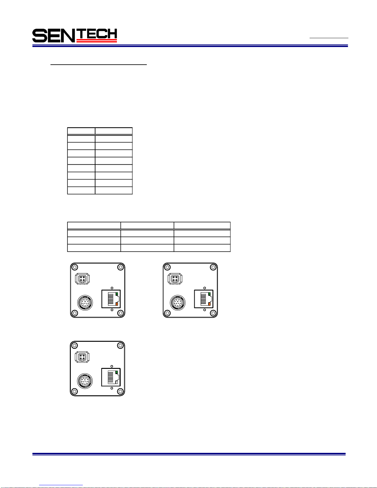
Caution: This product is a PoE type. Apply power (+10.8 to 26.4Vdc) through the power/IO connector when PoE is
not supported.
Pin assignment
Note. Power supply connection comprise PoE (IEEE802.3af).
LED information
Power ON the camera Green LED: Blinking
1Gb transferring
Yellow LED: OFF, Green LED: Blinking 100Mb transferring
NIC, HUB or LAN cable is not support 1Gb. Please use 1Gb supported NIC, HUB and LAN cable.
Please check the NIC and HUB setting is “1Gb transferring” when use with 1Gb supported NIC and
HUB.
When snapping of the CAT5e cable, possibility to change the transferring speed from 1Gb to 100Mb.
Please change the CAT5e cable.
Pin No.
Signal name
1
TA+
2
TA-3TB+
4 TC+
5
TC-
6 TB-
7
TD+
8 TD-
Yellow LED
Green LED
Status
Orange light ON Green light ON
Power ON
Orange light ON
Green light blinking 1Gb transfering
Light OFF
Green light blinking 100Mb transfering
Page 7
No.11S098-03
7
STC-GE33OX/GEC33OX
Users guide Rev. 1.03
1.2. Power/IO connector
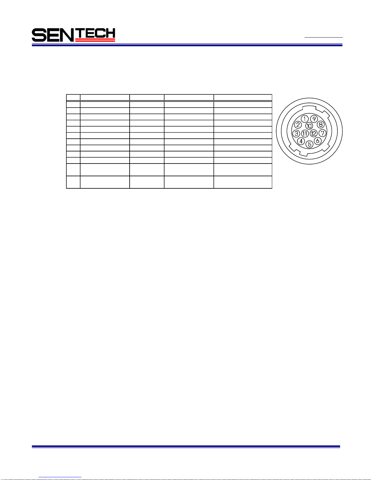
Connector: HR10A-10R-12PB (Hirose) or equivalent.
This connector is for DC power input and the input and output signals.
Pin assignment
Note.1: All I/Os (Pin number 3 through 10) are user assignable.
Note.2: DO NOT connect or disconnect the power/IO connector while the power input though PoE.
No. Signal type IO direction Spec. Initial signal
1 POWER IN GND - GND -
2 POWER IN - +10.8 to 26.4Vdc -
3 OUT0_AUX_OP OUT Opt. Isolated FrametriggerWait out
4 OUT1_AUX_OP OUT Opt. Isolated ExposureActive out
5 OUT2_AUX_OP OUT Opt. Isolated Open
6 OUT3_AUX_OP OUT Opt. Isolated Open
7 OUT4_AUX_OP OUT Opt. Isolated Open
8 IN0_AUX_OP IN Opt. Isolated TRG In
9 IN1_AUX_OP IN Opt. Isolated Open
10 IN2_AUX_OP IN Opt. Isolated Open
11 IO VCC IN - IO VCC -
+3 to +26.4Vdc
12 IO GND - IO GND -
Refer Fig. 3
12pin connector
Page 8

No.11S098-03
8
STC-GE33OX/GEC33OX
Users guide Rev. 1.03
1.2.1 Input signal
TRG IN: Input the trigger signal
High: Voltage of the “IO VCC IN”
Low: Smaller than 0.4V
1.2.2 Output signals
Set the output signals from the power/IO connector.
The following six output signals are selectable with the software or communication.
A) FrameTriggerWait
The user can check the camera conditions, which are the camera expose and the image output
processing by the trigger signal with this FrameTriggerWait signal.
a) High status (Voltage of the “IO VCC IN”): No processing by the trigger signal
The camera accepts the trigger signal
b) Low status (0V): The camera is expose and the image output processing by
the trigger signal
The camera default setting is the input trigger signal is INVALID while low status for this signal.
When the exposure starts while the image output by next trigger signal, please change the camera setting
(Device code: 00H, Command: 13H) to accept the trigger signal while the image output.
The noise appears on the image when start exposure while the image output. In this case, please change
the “H reset” for the exposure start mode (Device code: 00H, Command: 12H) to change the exposure
start point to next HD timing.
B) UserOutput
The status of this UserOutput signal can change with the “UserOutputValue”.
C) ExposureActive
The user can check the exposure time with this ExposureActive signal.
a) High status (Voltage of the “IO VCC IN”): The camera is exposing
b) Low status (0V): The camera is not expose
D) TriggerAuxiliary
This TriggerAuxiliary signal is the input trigger signal.
E) TriggerInternal
This TrigerInternal signal is the input trigger signal with the trigger delay time.
F) SensorReadOut
This SensorReadOut signal is the FVAL signal, which is the image output period of the time.
G) StrobeSignal
The StrobeSignal signal is the strobe control signal.
Page 9
No.11S098-03
9
STC-GE33OX/GEC33OX
Users guide Rev. 1.03
1.3. DC IRIS lens connector
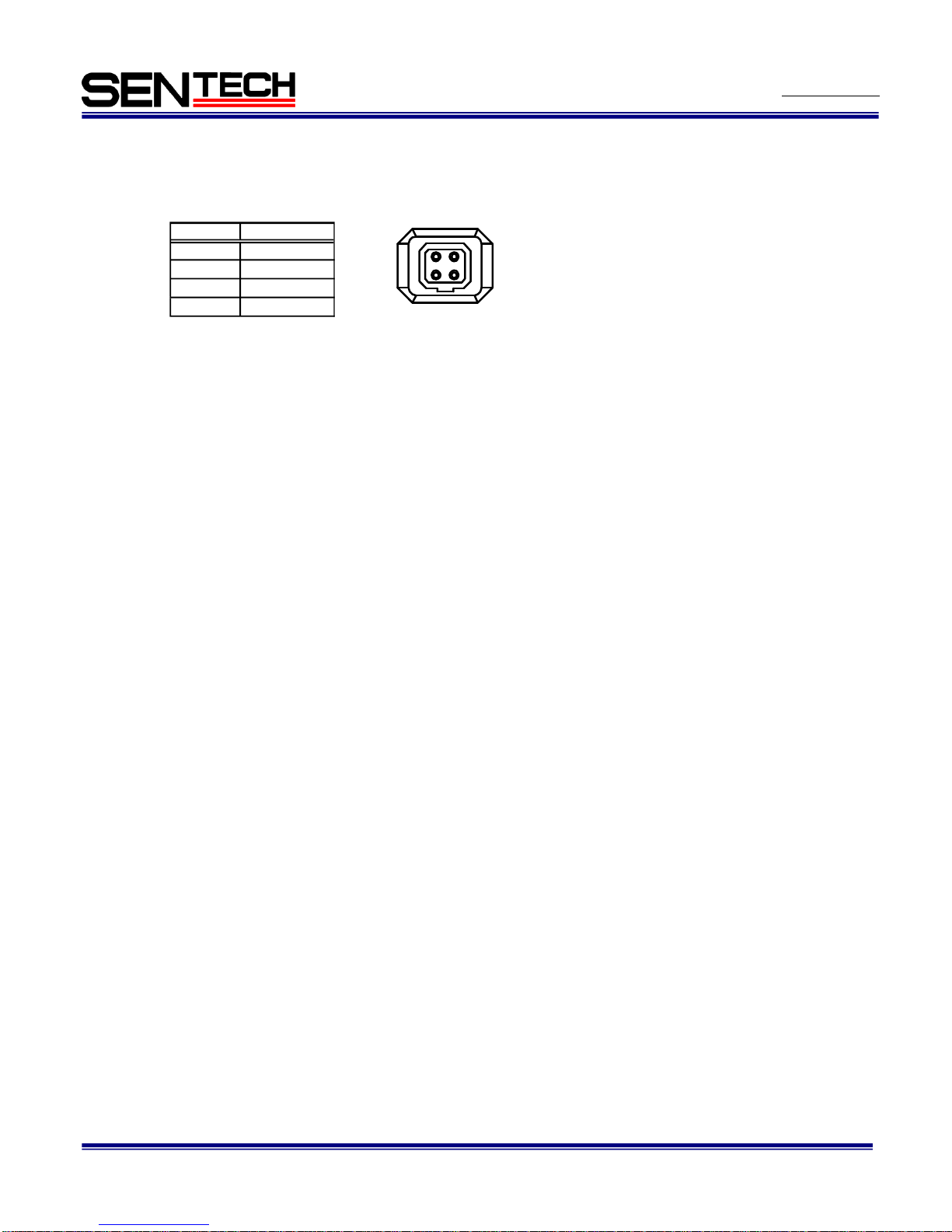
Connector: M1951 (EMUDEN) or equivalent.
Pin assignment
1 2
3 4
Pin No.
Signal name
1
DAMP-
2
DAMP+
3
DRIVE+
4 DRIVE-
Page 10
No.11S098-03
10
STC-GE33OX/GEC33OX
Users guide Rev. 1.03
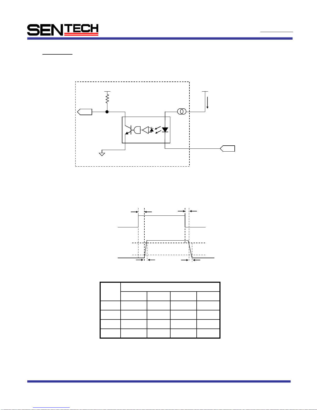
2 I/O circuits
2.1 Input circuit
Response timing
Input circuits
CAMERA
Response time
11[ns]
11[ns]
11[ns]
11[ns]
Tf
520[ns]
545[ns]
584[ns]
689[ns]
Ts
100[ns]
100 [ns]
100[ns]
100[ns]
Tr
3.0[us]
3.0[us]
2.8 [us]
2.5[us]
Td
24[V]
12[V]
5.0[V]
3.3[V]
IO_VCC
10%
90%
Td
Ts
Tr
Tf
USER INPUT
INPUT
OPTO ISOLATOR
SHARP:PC400J00000F
IO_VCC
CAM_VCC
If
INPUT
USER_INPUT
Maximum consumption of If is 6 mA
Page 11
No.11S098-03
11
STC-GE33OX/GEC33OX
Users guide Rev. 1.03
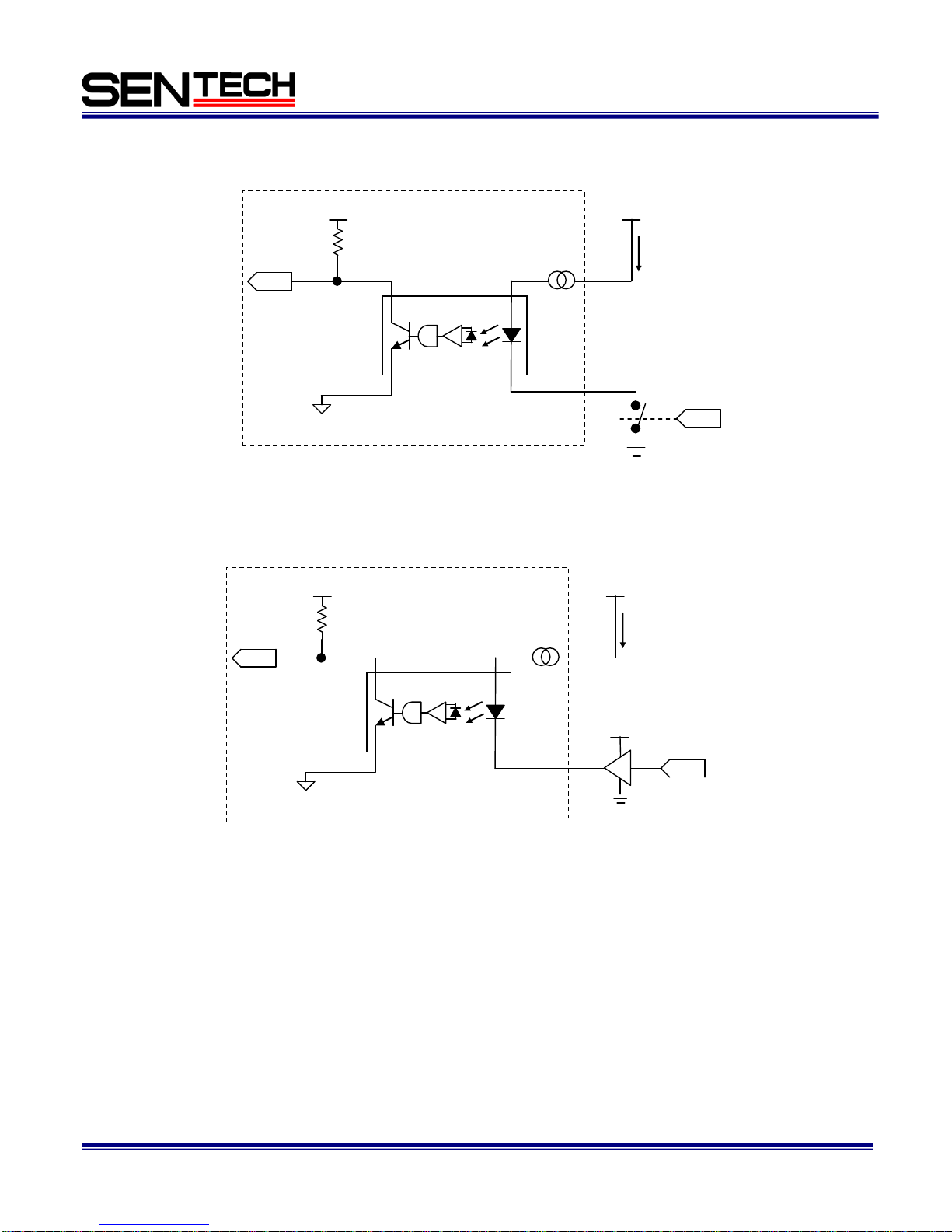
Example circuit for the input signal
USER_INPUT
OPTO ISOLATOR
SHARP:PC400J00000F
IO_VCC
CAMERA
CAM_VCC
IO_GND
If
INPUT
OPTO ISOLATOR
SHARP:PC400J00000F
IO_VCC
CAMERA
CAM_VCC
IO_GND
If
INPUT
IO_VCC
USER_INPUT
Page 12
No.11S098-03
12
STC-GE33OX/GEC33OX
Users guide Rev. 1.03
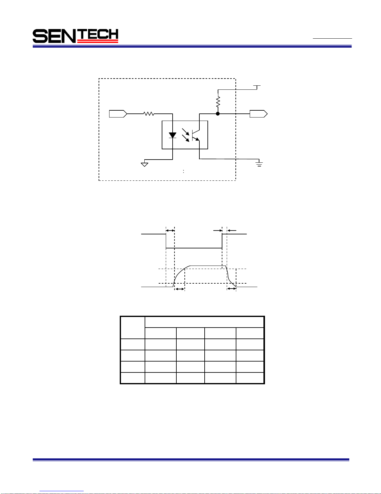
2.2 Output circuit
Response timing
Output circuits
OPTO ISOLATOR
SHARP PC354NJ0000F
IO_VCC
USER_OUTPUT
OUTPUT
IO_GND
10k Ohm
CAMERA
Ts
Td
10%
90%
Tr
Tf
OUTPUT
USER_OUTPUT
Response time
10.9[us]
6.9[us]
3.8[us]
3.1[us]
Tf
2.8[us]
2.8[us]
2.2[us]
2.2[us]
Ts
31.0[us]
42.3[us]
60.2[us]
67.5[us]
Tr
28.4[us]
35.2[us]
30.4 [us]
29.6[us]
Td
24[V]
12[V]
5.0[V]
3.3[V]
IO_VCC
Page 13
No.11S098-03
13
STC-GE33OX/GEC33OX
Users guide Rev. 1.03
3 User configurable FPGA (XILINX)
The customer would program the provided FPGA (XILINX) with its own proprietary code and the customer would
also have complete control over the “Memory” utilization.
Sentech checks the camera for proper operation by “Disabling” around the customer’s code and memory control.
3.1 User configurable FPGA (XILINX) information
3.1.1 Device information
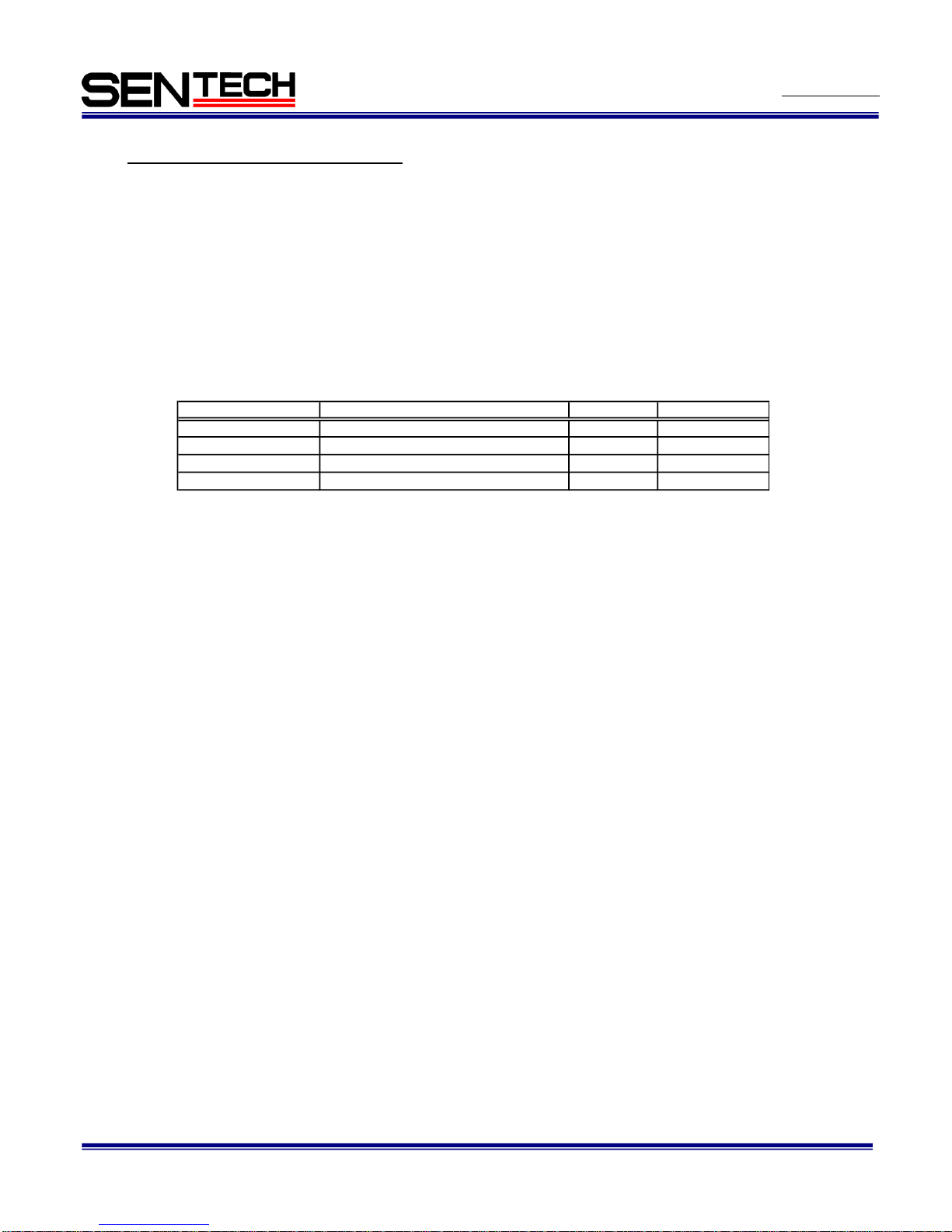
The manufacturer names and item numbers of the user configurable FPGA and the peripheral devices are
listed in the table-1.
3.1.2 User program examples
Implementation of proprietary algorithm
Image processing and conversion
Image storage
Image analysis
Pattern comparison and others
Device Part number Size Manufacture
FPGA XC3SD1800A (Package: CSG484) 1800 k gate XILINX
DDR2 W9725G6JB-25 32 MB Winbond
EEPROM M95512-RMN6TP 512 kbit ST Micro
Configuration ROM M25P80-VMP6G 8 Mbit Micron
(Table-1) FPGA and the peripheral devices
Page 14
No.11S098-03
14
STC-GE33OX/GEC33OX
Users guide Rev. 1.03
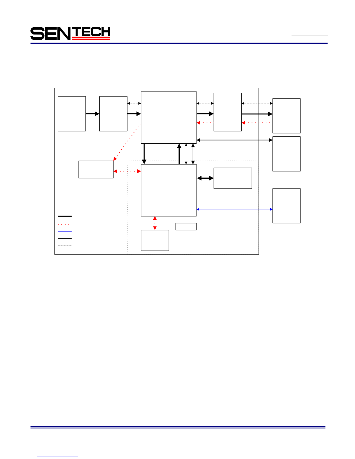
3.2 Block diagram and explanation
3.2.1 Block Diagram
CCD CDS/AD
Sentech
FPGA
Gig-E
I/F
User configuration
FPGA (XILINX)
Camera
Gigabit-
Ethernet
port
DDR2
Memory
(32MB)
Image data
UART
User configuration
FPGA (XILINX) area
Configuration
SPI BUS
EEPROM
(512Kbit)
Configuration
ROM (8Mbit)
12bit image data
Clock/FVAL/LVAL
25MHz
Power/IO
connector
JTAG
connector
3 inputs
5 outputs
JTAG
(TCK, TMS, TDI, TDO)
I/O
JTAG
Fig.1 Block diagram
Page 15

No.11S098-03
15
STC-GE33OX/GEC33OX
Users guide Rev. 1.03
3.2.2 Explanations of data flows
3.2.2.1 Image data
3.2.2.1.1 Image data flow
1) The analog image signal created by the CCD is processed through CDS (Correlated Double Sampling)
section and then is converted into digital data by the A/D converter.
2) This data is sent to "Sentech FPGA" for further processing.
3) Once the data is sent into "Sentech FPGA", the image data can be routed to "User Configurable FPGA".
Three different extraction points are provided in "Sentech FPGA" for this purpose. Please see
Section-3.2.2.1.2-2) for more details.
4) This data is further processed by the program you create in "User Configurable FPGA".
5) Now, the data should be returned to "Sentech FPGA". In this process, again, three different points are
provided in "Sentech FPGA" to return the data to. Please see Section-3.2.2.1.1. 3) for more details.
6) The data is sent to "GigE I/F (Interface)" and sent out through the Ethernet connector.
Page 16
No.11S098-03
16
STC-GE33OX/GEC33OX
Users guide Rev. 1.03
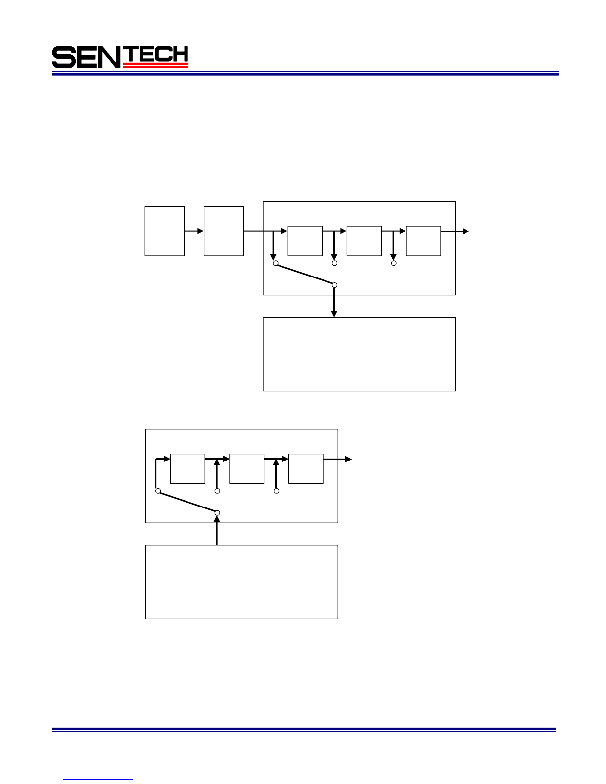
3.2.2.1.2 Image data extraction and insertion
The image data generated by the CCD is converted into 12-bit digital data as the section 3.2.2.1.1
explained. Then this data is extracted into the user FPGA, processed and inserted back to Sentech
FPGA.
1) Image data flow block diagram
CCD CDS/AD
Sentech
FPGA
User configurable
FPGA (XILINX)
DIN0 - 11
White
Balance
Gamma
Color
Interpolation
The image data from Sentech FPGA to user configurable FPGA
A B C
Sentech
FPGA
User configurable
FPGA (XILINX)
DOUT0 - 11
White
Balance
Gamma
Color
Interpolation
The image data from user configurable FPGA to Sentch FPGA
CBA
Fig. 2 Image data flow block diagram
Page 17

No.11S098-03
17
STC-GE33OX/GEC33OX
Users guide Rev. 1.03
2) Data extraction from Sentech FGPA
The 12-bit image data is extracted from Sentech FPGA as DIN11-0 into the user FPGA from any points
listed below. These points A, B and C are indicated in fig.2 (Image data flow block diagram).
A) For the color camera
A. CCD raw data
B. Data after the white balance processing
C. Data after the white balance and the gamma processing
B) For the color camera
A or B. CCD raw data
C. Data after the gamma processing
3) Data extraction from user configurable FGPA
After processing the 12-bit image data in the user FPGA, the data is inserted back to the Sentech FPGA
as DOUT11-0 at any points listed below. These points A, B and C are, again, indicated in fig.2 (Image
data flow block diagram).
A) For the color camera:
A. Before the white balance, the gamma and color interpolation processing
B. Before the gamma and the color interpolation processing
C. Before the color interpolation processing
B) For the monochrome camera
A or B Before the gamma processing
C Before the output from the camera (No processing)
4) Data assignment list
Please see section 3.3 for the data assignment.
It is not necessary to consider these data pin assignments if use the pin assignment and the timing
constraints file (Power_plus_000.ucf).
Page 18
No.11S098-03
18
STC-GE33OX/GEC33OX
Users guide Rev. 1.03
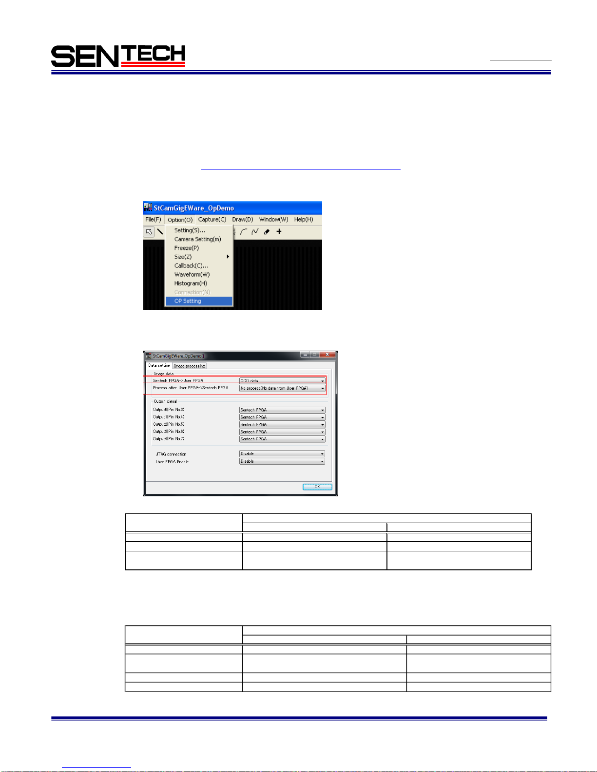
5) Image data switching method
As explained in the section 3.2.2.1.2, there are three points to extract out the image data from the
Sentech FPGA and the image process at Sentech FPGA after the image data send back from the user
configurable FPGA. There are two different methods to achieve this switching.
A) By using Sentech GUI “StCamGigEWare_OpDemo”
Also please see User configurable FPGA (XILINX) Sample Codes.
a) Select “OP Setting” under “Option” in the menu.
b) Select which image data sends from “Sentech FPGA” to “User configurable FPGA” at
“Sentech FPGA -> User FPGA”
c) Select the image process at Sentech FPGA after the image data send back from “User configurable
FPGA” at “Process after User FPGA -> Sentech FPGA”
Selection
Color camera Monochrome camera
CCD data CCD raw data CCD raw data
White balance processed data White balance processed image data CCD raw data
White balance and White balance processed and Gamma processed image data
gamma processed data gamma processed image data
Image data from Sentech FPGA
Selection
Color camera Monochrome camera
No process No image data from the User FPGA No image data from the User FPGA
White balance, gamma and White balance, gamma and Gamma processing
color interpolation color interpolation processing
Gamma and color interpolation Gamma and color interpolation processing Gamma processing
Color interpolation color interpolation processing No processing
Image process at Sentech FPGA after the image data send back from User FPGA
(Table-2) Image data selection from Sentech FPGA
(Table-3) Image process at Sentech FPGA
Page 19

No.11S098-03
19
STC-GE33OX/GEC33OX
Users guide Rev. 1.03
B) By changing the register value through the UART
Also please see section “6 The communication protocol specifications”.
a) Set the image data between FPGAs (Device code: 20H, command: C0H).
Page 20
No.11S098-03
20
STC-GE33OX/GEC33OX
Users guide Rev. 1.03
3.2.2.2 Configuration data
1) The FPGA program created by users is sent to "Configuration ROM" through the Ethernet connector as
"Configuration data".
2) The data is sent through "GigE I/F" and "Sentech FPGA" to "Configuration ROM" and stored.
(Note) Please see “User configurable FPGA (XILINX) uploading instructions” for more detailed
information.
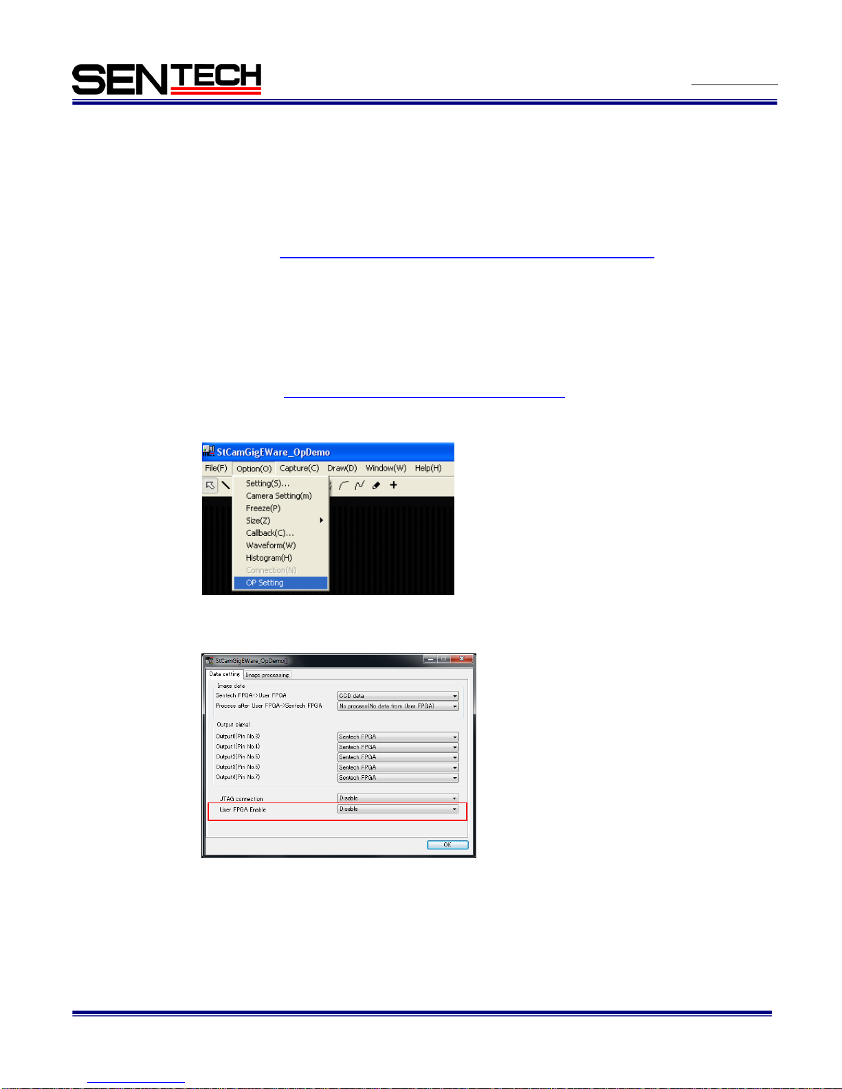
3) Select “Enable” at “User FPGA Enable” when the user configurable FPGA has to configure with the
uploaded configure data for the user configurable FPGA.
The user configurable FPGA does not work if select “Disable” at “User FPGA Enable”.
A) By using Sentech GUI “StCamGigEWare_OpDemo”
Also please see User configurable FPGA (XILINX) Sample Codes.
a) Select “OP Setting” under “Option” in the menu.
b) Select which image data sends from “Sentech FPGA” to “User configurable FPGA” at
“Sentech FPGA -> User FPGA”
B) By changing the register value through the UART
Also please see section “6 The communication protocol specifications”.
a) Set 01H for the “Use FPGA Enable” (Device code: 20H, command: 19H).
Page 21
No.11S098-03
21
STC-GE33OX/GEC33OX
Users guide Rev. 1.03
3.2.2.3 JTAG
1) This JTAG connection is provided for the debugging procedures of the "User Configurable FPGA" program.
JTAG connector is connected to "User Configurable FPGA".
(Note) The rear panel of the camera masks JTAG connector. Rear panel kit is available from Sentech for
JTAG accessibility.
(Note) Please see “User configurable FPGA (XILINX) JTAG accessing instructions” for more detailed
information.
3.2.2.4 User I/Os
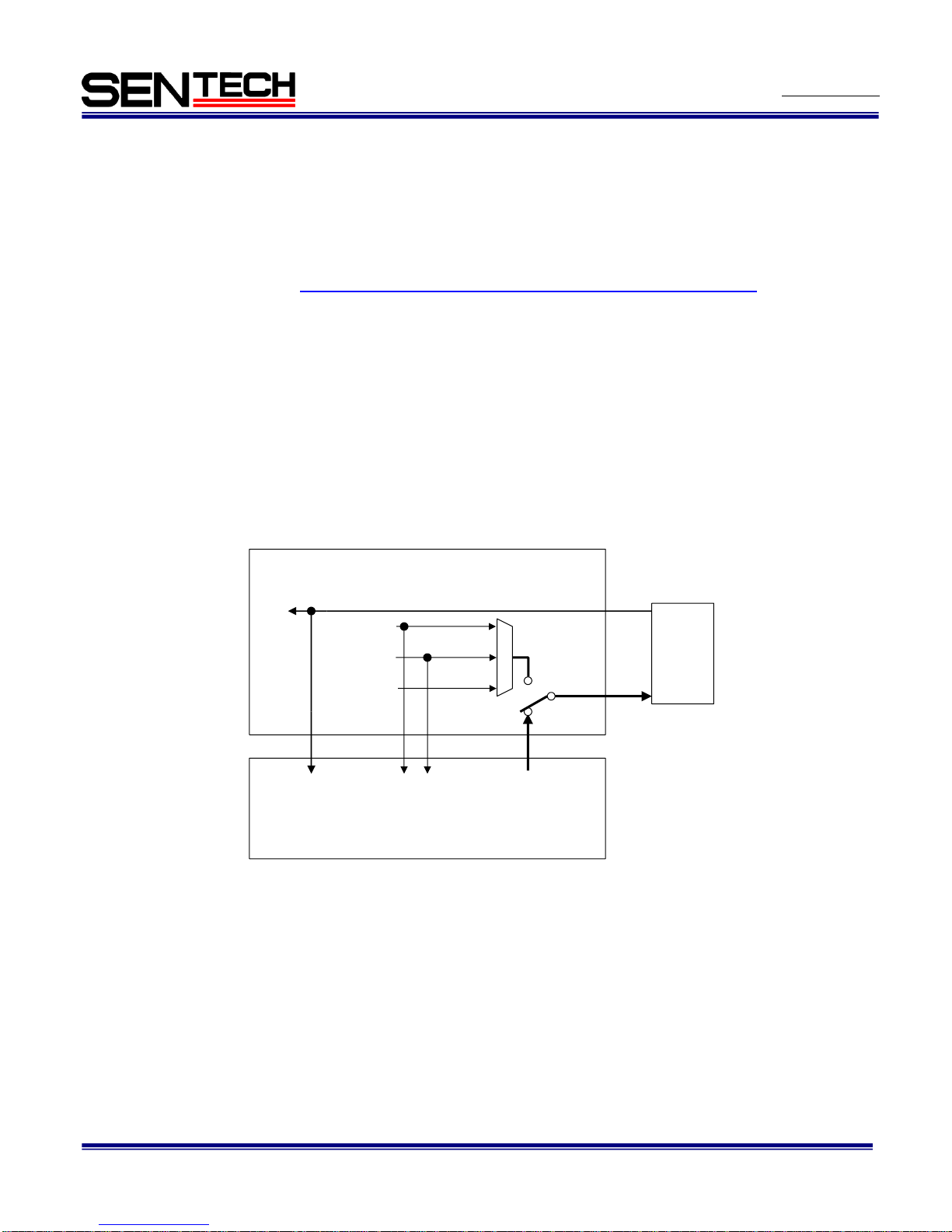
The camera provides total of eight I/O points. Three are designated as inputs and five as outputs. Each I/O
point can be assigned (or connected) to any points in "Sentech FPGA" or "User Configurable FPGA".
Please see table-4 and 2 I/O circuits for more details.
(Note) Input’s assignments in the Sentech FPGA are limited for the functions of “Exposure out” and “Trigger
ready”.
1) Conceptual I/O connection diagram
Fig. 3 User I/Os diagram
Sentech FPGA
User configurable FPGA (XILINX)
IN x 3
Power/IO
connector
ExposureActive
FrameTriggerWait
Other OUTs
TRG IN
Other 2 IN
OUT x5
IN x3
x5
OUT x5IN x3
ExposureActive FrameTriggerWait
Page 22
No.11S098-03
22
STC-GE33OX/GEC33OX
Users guide Rev. 1.03
2) I/O port switching method
There are two different methods to achieve this switching.
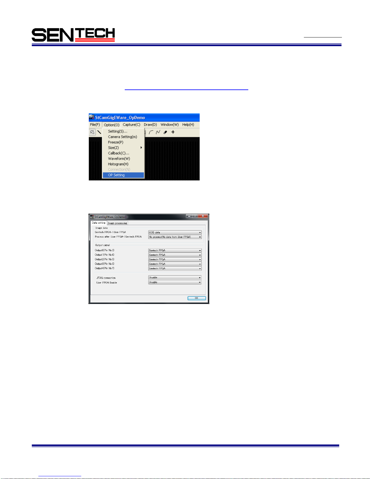
A) By using Sentech GUI “StCamGigEWare_OpDemo”
Also please see User configurable FPGA (XILINX) Sample Codes.
a) Select “OP Setting” under “Option” in the menu.
b) Select which FPGA (Sentech FPGA or user configurable FPGA) send the output signal to 12pin
power/IO connector at I/O Out0 to I/O Out4.
In case of above window:
Sentech FPGA send output signals to Output 1 and 2 of 12pin power/IO connector.
User configurable FPGA send output signals to Output 3, 4 and 5 of 12pin power/IO connector.
B) By changing the register value through the UART
Also please see section “6 The communication protocol specifications”.
a) Set the output signal selection (Device code: 20H, command: C1H).
Select the output signal from the Sentech FPGA or the user configurable FPGA for each output.
b) Set the signals of the Power/IO connector (Device code: 00H, command: F0H, F8H and F9H).
Select the output signal from the Sentech FPGA when select output signal from the Sentech FPGA.
Page 23
No.11S098-03
23
STC-GE33OX/GEC33OX
Users guide Rev. 1.03
3.2.2.5 UART through Ethernet connector
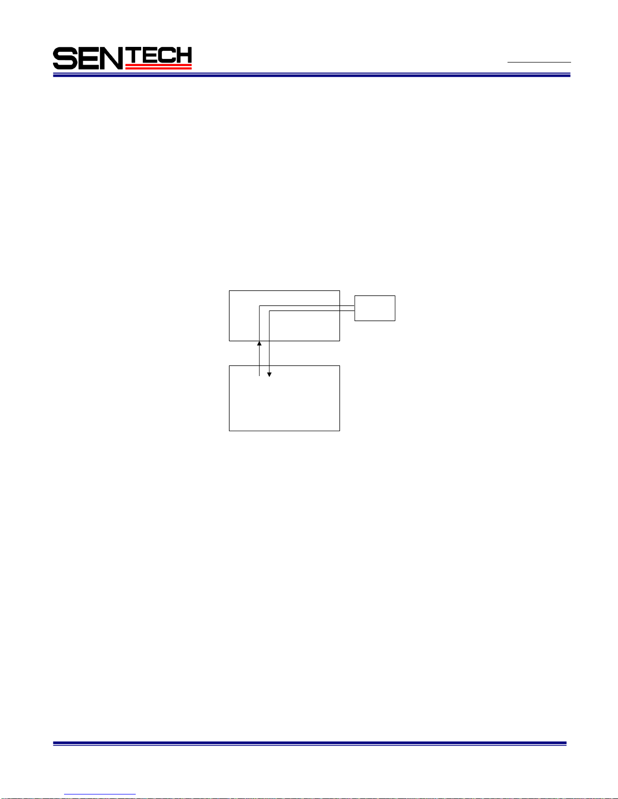
The camera provides a serial communication channel (UART1) through Ethernet connector for the user
configurable FPGA. Through this communication channel, you can change register values in "User
configurable FPGA".
1) Please change the UART port from the UART0 to the UART1.
1) Please setup UART port as following
Baud rate: 115,200bps
Data bit: 8bit
Parity: None
Stop bit: 1bit
Flow control: None
Fig. 4 UART diagram
Sentech FPGA
User configurable
FPGA (XILINX)
Ethernet
connector
USER_
TXD_PC
USER_
RXD_PC
Page 24
No.11S098-03
24
STC-GE33OX/GEC33OX
Users guide Rev. 1.03
3.2.3 Important design consideration of data timing and handling
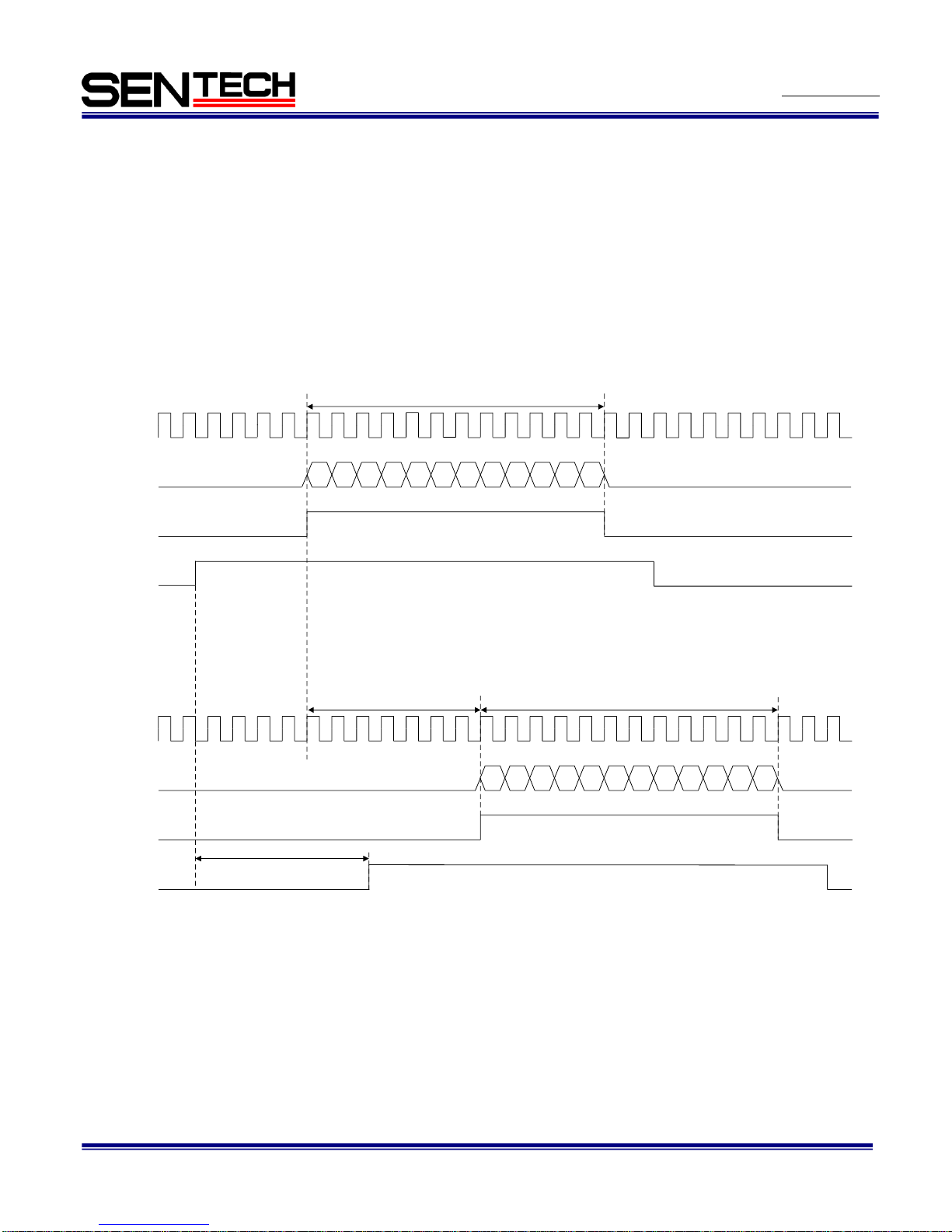
In the design process of the video processing program, follow the below conditions of the data timings.
1) DIN (image data), LVALIN and FVALIN are activated at the rising edges of CLKIN as the data comes into the
user FPGA.
2) As the data sent back to the Sentech FPGA, add the delay equivalent to the process time in the user FPGA
on LVALIN and FVALIN.
3) As the data is sent back to the Sentech FPGA, DIN (image data), LVALIN and FVALIN must be activated at
the rising edges of CLKIN.
CLKIN: 36.81MHz
CLKIN
DIN [11:0]
LVALIN
FVALIN
D0 D1 D2 D3 D4 Dx
CLKIN
DOUT [11:0]
LVALOUT
FVALOUT
D0 D1 D2 D3 D4 Dx
Number of clock for
image processing
Number of clock for
image processing
Number of pixel in 1 horizontal
Number of pixel in 1 horizontal
Fig. 5 The image data input timing to user configurable FPGA
Fig.6 The image data output timing form user configurable FPGA after image processing
Page 25
No.11S098-03
25
STC-GE33OX/GEC33OX
Users guide Rev. 1.03
3.3 Connection information between the devices
It is not necessary to consider these data pin assignments if use the pin assignment and the timing constraints file
(power_plus_000.ucf).
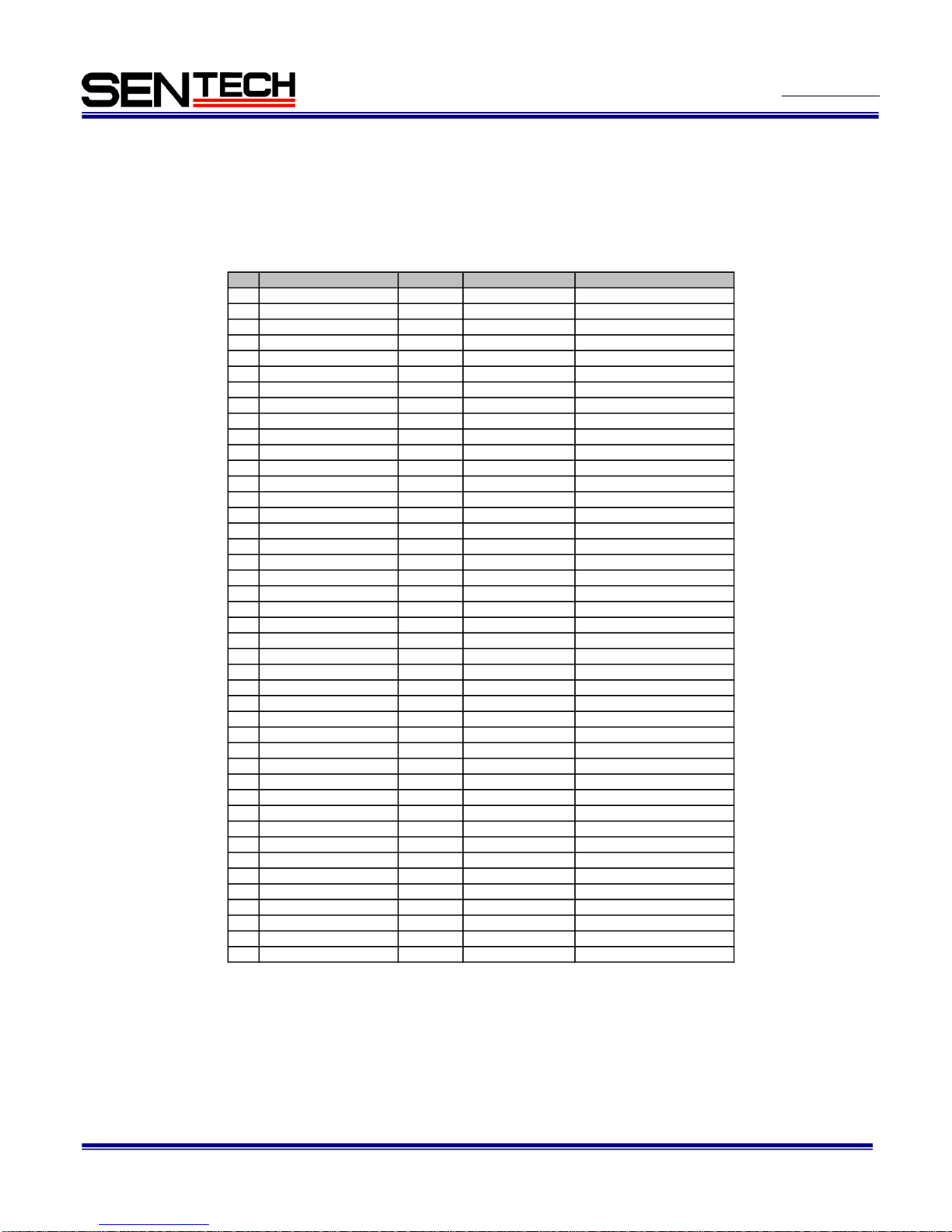
3.3.1 Connection between the user configurable FPGA (XILINX) and the Sentech FPGA
(Table-4) Connection between the user configurable FPGA (XILINX) and the Sentech FPGA
No Signal Name Direction Discription Pin No. of User FPGA
1 DIN0 input Image Data bit0 B6
2 DIN1 input Image Data bit1 A6
3 DIN2 input Image Data bit2 A7
4 DIN3 input Image Data bit3 A5
5 DIN4 input Image Data bit4 B3
6 DIN5 input Image Data bit5 B4
7 DIN6 input Image Data bit6 A3
8 DIN7 input Image Data bit7 A4
9 DIN8 input Image Data bit8 A8
10 DIN9 input Image Data bit9 B11
11 DIN10 input Image Data bit10 B8
12 DIN11 input Image Data bit11 A11
13 FVALIN input FVAL C13
14 LVALIN input LVAL C15
15 DOUT0 output Image Data bit0 B13
16 DOUT1 output Image Data bit1 B15
17 DOUT2 output Image Data bit2 A16
18 DOUT3 output Image Data bit3 A9
19 DOUT4 output Image Data bit4 A17
20 DOUT5 output Image Data bit5 B9
21 DOUT6 output Image Data bit6 C4
22 DOUT7 output Image Data bit7 C6
23 DOUT8 output Image Data bit8 C7
24 DOUT9 output Image Data bit9 C8
25 DOUT10 output Image Data bit10 C9
26 DOUT11 output Image Data bit11 C12
27 FVALOUT output FVAL A13
28 LVALOUT output LVAL A14
29 CLKIN input CLK F11
30 SYS_RST_N input SYSTEM_RESET AA12
31 USER_TXD_PC input UART_TX E22
32 USER_RXD_PC output UART_RX G22
34 USER_OUT_AUX0 output USER_I/O P22
35 USER_OUT_AUX1 output USER_I/O R22
36 USER_OUT_AUX2 output USER_I/O R20
37 USER_OUT_AUX3 output USER_I/O U22
38 USER_OUT_AUX4 output USER_I/O V20
39 USER_IN_AUX0 input USER_I/O W22
40 USER_IN_AUX1 input USER_I/O Y22
41 USER_IN_AUX2 input USER_I/O W19
42 ExposureActive input EXP_OUT N17
43 FrameTriggerWait input TRG_RDY N18
44 USER_TRG output TRG_OUT D22
Page 26

No.11S098-03
26
STC-GE33OX/GEC33OX
Users guide Rev. 1.03
(Note) Signal directions indicated as inputs and outputs are referencing to the user FPGA. “Input” means a
signal from the Sentech FPGA to the user FPGA and “output” means from the user FPGA to Sentech
FPGA.
Image data transferred between the Sentech FPGA and the user FPGA is 12-bit data. The MSB (Most
Significant Bit) is bit-11 and the LSB (Least Significant Bit) is bit-0. “DIN0-11”is the data from the Sentech
FPGA to the user PGA, and “DOUT0-11” is the data from the user PGA to the Sentech FPGA.
Please sets Float, Pull-up or Pull-down for unused input signal of the user configurable FPGA.
Please sets Pull-up or Pull-down, or sets [H] or [L] with RTL code, for unused output signal of the user
configurable FPGA.
Page 27
No.11S098-03
27
STC-GE33OX/GEC33OX
Users guide Rev. 1.03
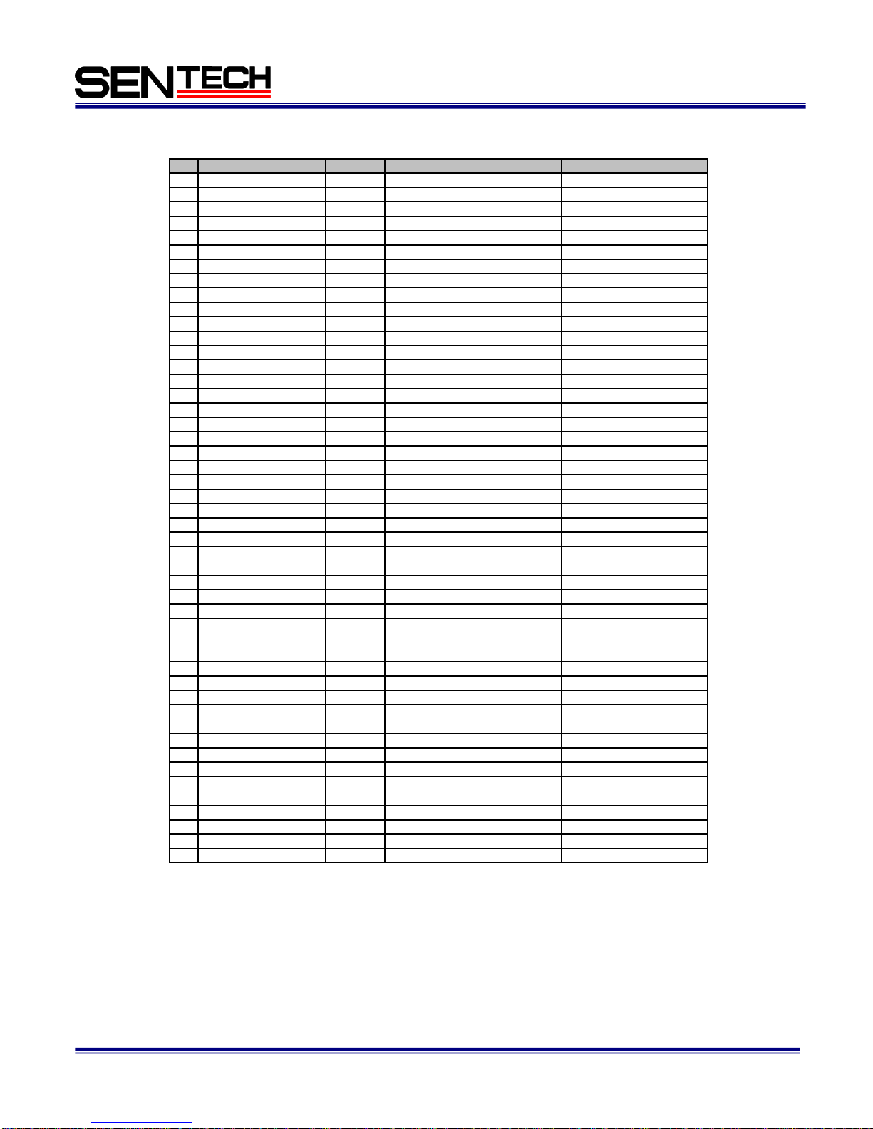
3.3.2 Connection between user configurable FPGA (XILINX) and DDR2
(Note) Signal directions indicated as inputs and outputs are referencing to the user FPGA. “Input” means a
signal from the DDR2 to the user FPGA and “output” means from the user FPGA to DDR2.
Please sets Float, Pull-up or Pull-down for unused input and I/O signal of the user configurable FPGA.
Please sets Pull-up or Pull-down, or sets [H] or [L] with RTL code, for unused output signal of the user
configurable FPGA.
(Table-5) Connection between user configurable FPGA (XILINX) and DDR2
No Signal Name Direction Discription Pin No. of User FPGA
1 DDR_A0 output Address0 G1
2 DDR_A1 output Address1 K5
3 DDR_A2 output Address2 K4
4 DDR_A3 output Address3 L5
5 DDR_A4 output Address4 K6
6 DDR_A5 output Address5 K3
7 DDR_A6 output Address6 K2
8 DDR_A7 output Address7 M5
9 DDR_A8 output Address8 L6
10 DDR_A9 output Address9 V3
11 DDR_A10 output Address10 V4
12 DDR_A11 output Address11 W2
13 DDR_A12 output Address12 W3
14 DDR_A13 - Not use F1
15 DDR_A14 - Not use F5
16 DDR_A15 - Not use F4
17 DDR_BA0 output Bank address0 H5
18 DDR_BA1 output Bank address1 H1
19 DDR_BA2 - Not use H2
20 DDR_D0 I/O Data0 Y1
21 DDR_D1 I/O Data1 W1
22 DDR_D2 I/O Data2 R3
23 DDR_D3 I/O Data3 T4
24 DDR_D4 I/O Data4 T1
25 DDR_D5 I/O Data5 R5
26 DDR_D6 I/O Data6 T6
27 DDR_D7 I/O Data7 T5
28 DDR_D8 I/O Data8 P6
29 DDR_D9 I/O Data9 P2
30 DDR_D10 I/O Data10 P1
31 DDR_D11 I/O Data11 N5
32 DDR_D12 I/O Data12 L3
33 DDR_D13 I/O Data13 M2
34 DDR_D14 I/O Data14 K1
35 DDR_D15 I/O Data15 L1
36 DDR_RAS# output Command inputs F4
37 DDR_CAS# output Command inputs G5
38 DDR_WE# input Command inputs G6
39 DDR_CKE output Clock enable H6
40 DDR_CK output Clock U4
41 DDR_CK# output Clock U5
42 DDR_LDQS I/O Data strobe for lower byte U2
43 DDR_LDQS# I/O Data strobe for lower byte V1
44 DDR_UDQS I/O Data strobe for upper byte M6
45 DDR_UDQS# I/O Data strobe for upper byte N7
46 DDR_ODT output On-die termination F2
47 DDR_LDM output Input data mask for lower byte U1
48 DDR_UDM output Input data mask for upper byte R6
Page 28
No.11S098-03
28
STC-GE33OX/GEC33OX
Users guide Rev. 1.03
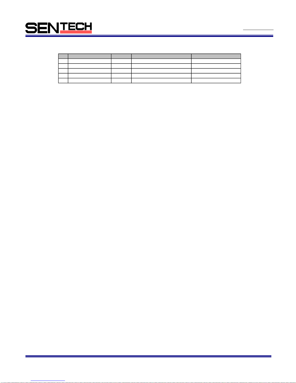
3.3.3 Connection between the user configurable FPGA (XILINX) and the EEPROM
(Note) Signal directions indicated as inputs and outputs are referencing to the user FPGA. “Input” means a
signal from the DDR2 to the user EEPROM and “output” means from the user FPGA to EEPROM.
Please sets Float, Pull-up or Pull-down for unused input signal of the user configurable FPGA.
Please sets Pull-up or Pull-down, or sets [H] or [L] with RTL code, for unused output signal of the user
configurable FPGA.
No Signal Name Direction Discription Pin No. of User FPGA
1 ROM_512KBIT_CLK output Serial Clock for ROM U20
2 ROM_512KBIT_nS output Chip Select for ROM T17
3 ROM_512KBIT_DATA output Serial Data input for ROM T20
4 ROM_512KBIT_Q input Serial Data output for ROM T18
5 ROM_512KBIT_nW output Write Protect for ROM R19
(Table-6) Connection between the user configurable FPGA (XILINX) and the EEPROM
Page 29
No.11S098-03
29
STC-GE33OX/GEC33OX
Users guide Rev. 1.03
3.4 Development guideline
3.4.1 Module and constraints files
3.4.1.1 Top file
Top file is Power_plus.001.v file. Assign own codes onto this file.
3.4.1.2 Pin assignment and the timing constraints file
Pin assignment and the timing constraints file is power_plus.000.ucf file.
Add all constraints of own design onto this constraints file.
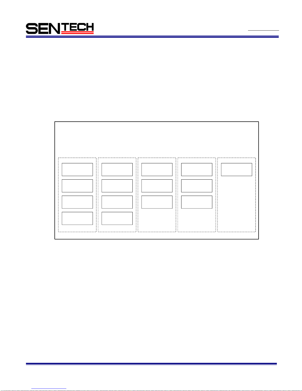
3.4.1.3 Structure of the sample code
3.4.2 Important design cautions
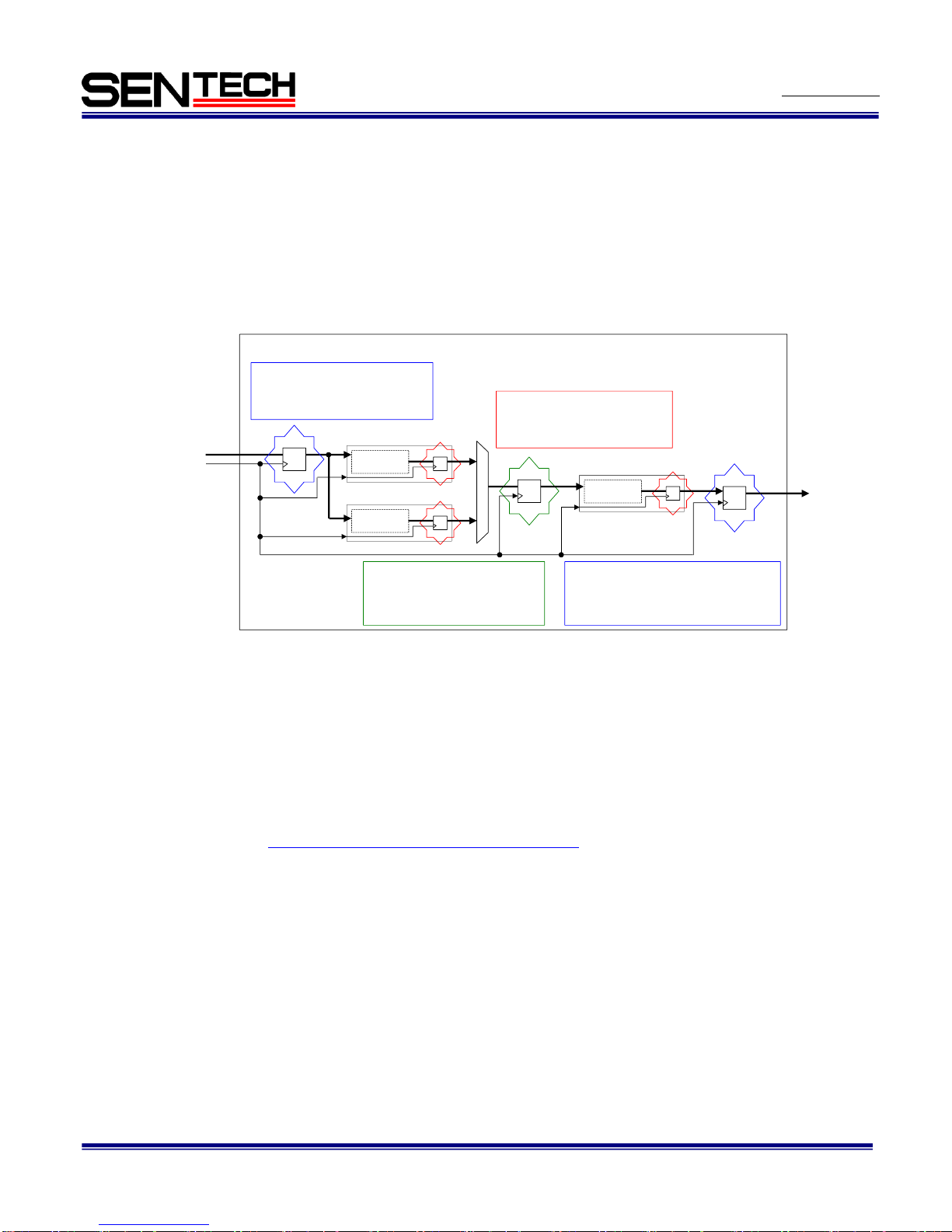
As you design the program in the user FPGA, it is essential to synchronize all processes to the clock pulse
rising edges given from the FPGA's pin number F11 (symbol CLKIN). Follow the four important notices listed
below along with the (Fig-8) Conceptual drawing of the FPGA programming.
Caution
1) Latch all signal timings of the image data, LVAL and FVAL coming from Sentech FPGA at the rising edges
of the clock pulse (symbol CLKIN).
2) In the same manner, the signal timings of the image data, LVAL and FVAL after image processing must be
latched at the rising edges of the clock pulse (symbol CLKIN).
3) When a selector is used in the process as shown as an example in the drawing, the signal timings of the
image data, LVAL and FVAL must be latched at the rising edges of the clock pulse (symbol CLKIN).
4) The image data, LVAL and FVAL must be latched at the rising edges of the clock pulse (symbol CLKIN)
before sending them back to Sentech FPGA.
dis_erea_number_top
(Verilog)
mig_dcm_ddr2
(Xilinx IP Core)
mig_ddr2_wrapper
(ngc)
frame_memory_cnt
(ngc)
bin_caluc_gc
(Verilog)
img_sig_delay_2c
(Verilog)
div_capture_bin
(Verilog)
gc_dis_number_top
(Verilog)
edge_detect_top
(ngc)
img_sig_delay_1line_7c
(Verilog)
div_capture
(Verilog)
uart_top
(ngc)
cnt_device_dna
(Verilog)
dis_device_dna
(Verilog)
DNA_PORT_inst
(Xilinx Library)
Top module
power_plus_001
(Veriolog)
Control Frame Memory
for DDR2 Function
Binarize &
Calculate
center of gravity
Function
Detect Edge
Function
Read Device DNA
Function
Recive UART
Function
Fig. 7 Structure of the sample code
Page 30
No.11S098-03
30
STC-GE33OX/GEC33OX
Users guide Rev. 1.03
3.4.3 Notice for use DDR2 memory
DDR2 memory control IP core for the sample code was made by MIG3.3 (Core Generator) with the below
settings.
The generated file
(¥ipcore_dir¥mig_dcm_ddr2¥mig_dcm_ddr2¥user_design¥par¥mig_dcm_ddr2_infrastructure_tip.v) was
changed as below:
The timing constraints file, which is made by the IP core belong to ISE
(¥ipcore_dir¥mig_dcm_ddr2¥mig_dcm_ddr2¥user_design¥par¥mig_dcm_ddr2.ucf) is reflect to the
power_plus_000.ucf file.
The optional setting of the ISE was changed as below from the default setting, to use DDR2 memory.
Setting Item Setting Value
Burst Length 4
Burst Type Sequential
Output Driver Strength Fullstrength
RTT(nominal)-ODT 75Ohm
DQS# Enable Enable
USE DCM check
Class for Address and Control Class II
Class for Data Class II
Debug Signal for Memory Controller Disable
System Clock Signal-Ended
105 line of mig_dcm_ddr2_infrastructure_top.v
/*
generate
if(`CLK_TYPE == "DIFFERENTIAL") begin : DIFF_ENDED_CLKS_INST
IBUFGDS_LVDS_25 SYS_CLK_INST
(
.I (sys_clk),
.IB (sys_clkb),
.O (sys_clk_ibuf)
);
end else if(`CLK_TYPE == "SINGLE_ENDED") begin : SINGLE_ENDED_CLKS_INST
IBUFG SYS_CLK_INST
(
.I (sys_clk_in),
.O (sys_clk_ibuf)
);
end
endgenerate
*/
// CHANGE BY SENSOR TECHNOLOGY
assign sys_clk_ibuf = sys_clk_in;
Category Property name Value
Synthesis Options
Keep Hierarchy
Soft
(Table-7) Setting of MIG3.3
(Table-8) Optional setting of ISE
Page 31
No.11S098-03
31
STC-GE33OX/GEC33OX
Users guide Rev. 1.03
3.4.4 Recommend the image data handle between the Sentech FPGA and the user configurable FPGA
Recommend to make the image processing with synchronize CLKIN when make the image processing in the
user configurable FPGA.
Recommend to set timing restriction for secure the timing margin of CLKIN and the image data (DIN, DOUT,
LVALIN, LVALOUT, FVALIN, FVALOUT) between the Sentech FPGA and the user configurable FPGA.
Please check the sample code for details.
3.4.5 Copy guard function
The user configurable FPGA (XILINX: XC3SD1800A) supports “Device DNA security function” for the FPGA
design protection.
The user configurable FPGA has 57 bit unique ID. This ID can use for the security key.
Please check the XILINX application note: WP266.
3.4.6 Schematics of the user configurable FPGA (XILINX)
Please check Schematics of user configurable FPGA (XILINX).
Image
processing 1
Image
processing 2
Image
processing 3
User configurable FPGA
The image data (DIN, LVALIN, FVALIN)
from the Sentech FPGA is
Flip-Flop output with the rising edge
of CLKIN after input image data
The image data (DIN, LALIN, FVALIN)
at each image processing is
Flip-Flop output with the rising edge
of CLKIN
When select the image data,
the image data (DIN, LVALIN, FVALIN)
is Flip-Flop output with the rising edge
of CLKIN after select the image data
The image data (DOUT, LVALOUT, FVALOUT)
to the Sentech FPGA is Flip-Flop output with the
rising edge of CLKIN
Output signals to
Sentech FPGA
DOUT [11:0]
LVALOUT
FVALOUT
Input signals from
Sentech FPGA
DIN
[11:0]
LVALIN
FVALIN
CLKIN
Fig. 8 Recommend image data handle
Page 32
No.11S098-03
32
STC-GE33OX/GEC33OX
Users guide Rev. 1.03
4 The camera output timing charts
4.1 The horizontal timing
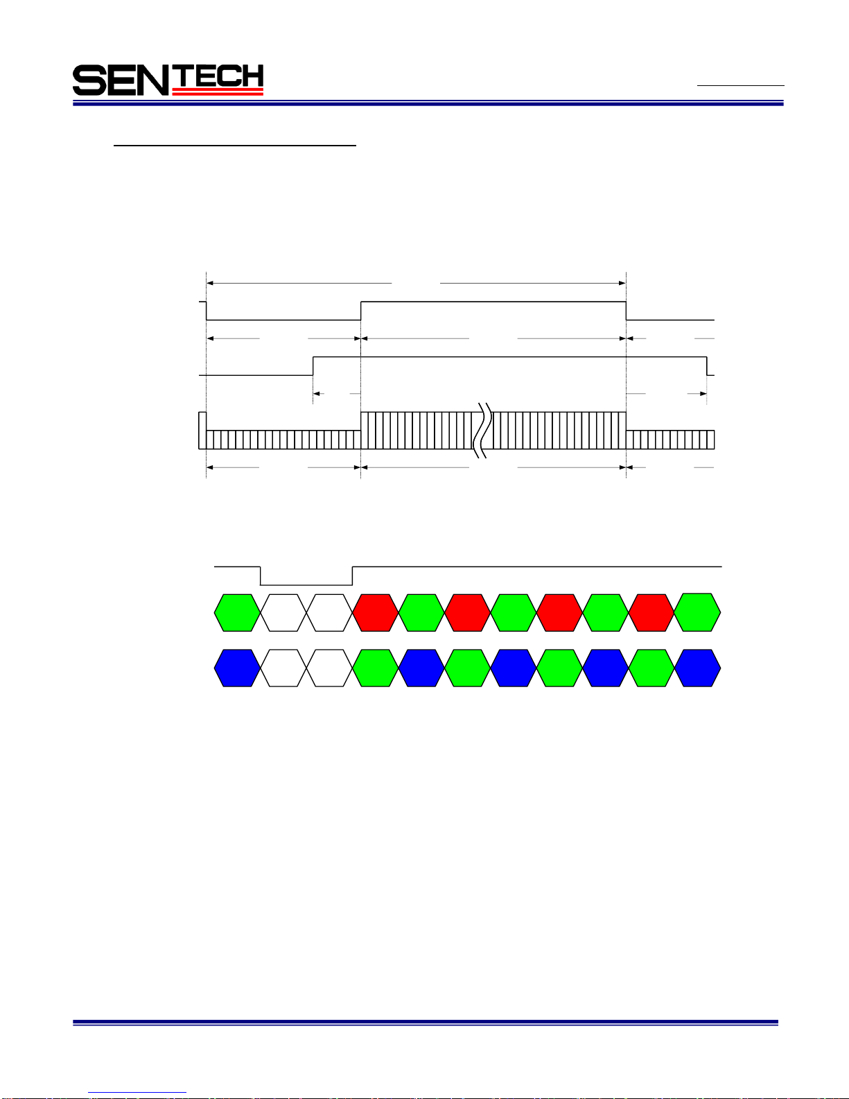
1 CLK = 27.1605 nseconds
4.1.1 Color Bayer order (This information is only for STC-GEC33OX)
R1 Gr1 R2
Gb1 Gb2B1
Gr2
B2
Video out
Line 1
・・・
Video out
Line 2
LVAL
R3
Gb3
Gr3B3・・・
・・・
・・・
・・・・・・
132 CLK648 CLK
Video out
LVAL
DVAL
Horizontal blanking
780 CLK
One horizontal (1H)
648 CLK132 CLK
132 CLK
Video output
132 CLK
94 CLK
38
CLK
FVAL
Page 33
No.11S098-03
33
STC-GE33OX/GEC33OX
Users guide Rev. 1.03
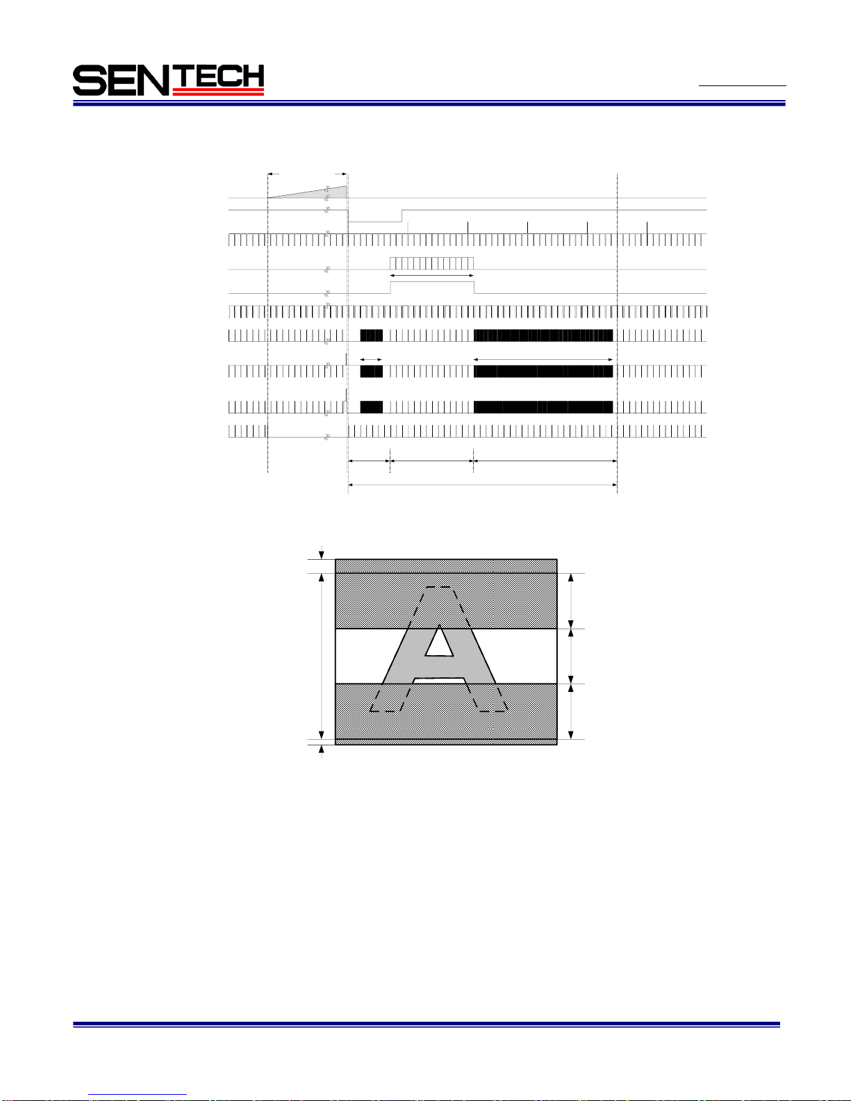
4.2 The vertical timing
4.2.1 Full scanning
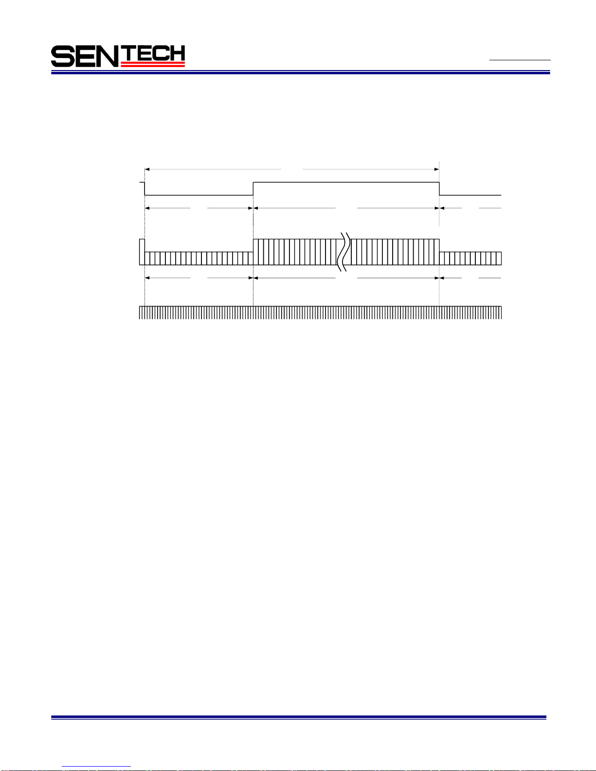
1 H = 21.1852 µseconds, 89.910172 Hz
31H494H
Video out
FVAL
Vertical blanking
525H
One vertical (1V)
494H31H
31H
Video output
1
2
493
494
31H
LVAL
Page 34
No.11S098-03
34
STC-GE33OX/GEC33OX
Users guide Rev. 1.03
4.2.2 AOI
Internal HD
Internal VD
Video out
EXT_TRIG
FIX_TRIG
(Common)
10 20 30 40 50
Exposure time
V1
V2
V3
SUB
FVAL
LVAL
Number of the
effective lines [Y]
High speed
transfer [X+a]
High speed transfer [f+g-X-Y]
Blanking (Front)
[BLK_F]
Number of the effective lines [Y]
Total number of the line at 1 frame [TOTAL_LINE]
Blanking (Back)
[BLK_B)
CCD effective
lines
Blanking
(Front)
Effective
lines
Optical black
+
Dummy bit
Blanking
(Back)
Optical black
Page 35
No.11S098-03
35
STC-GE33OX/GEC33OX
Users guide Rev. 1.03
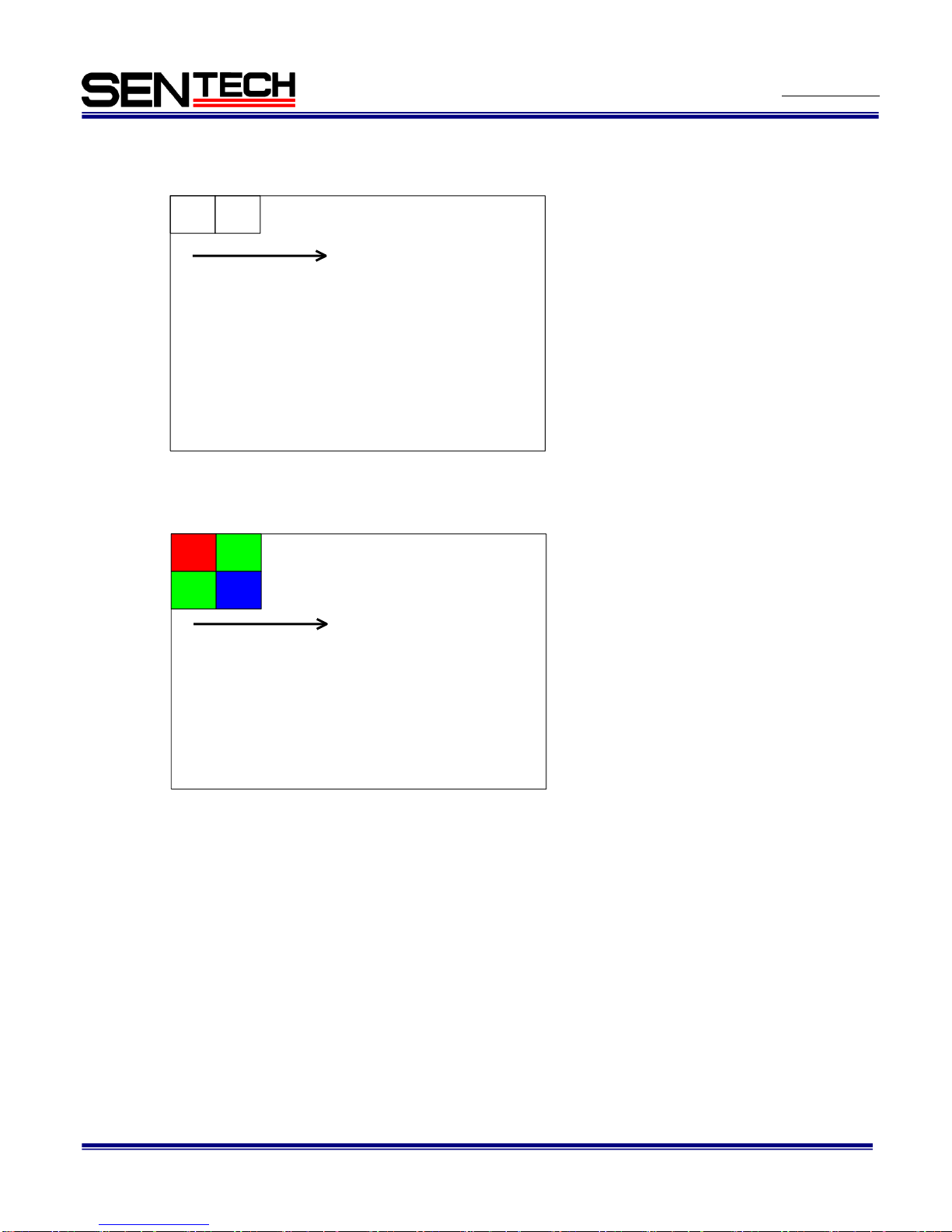
4.3 The transferring image
STC-GE33OX (Monochrome)
Pixeln of Data: The transferring pixel
n: The order number
STC-GEC33OX (Color)
Pixelmn of Data: The transferring pixel
m: The line number
n: The order number
Pixel1 of
Data
Pixel2 of
Data
Pixel11 of
Data
Pixe12 of
Data
Pixel21 of
Data
Pixel22 of
Data
Page 36
No.11S098-03
36
STC-GE33OX/GEC33OX
Users guide Rev. 1.03
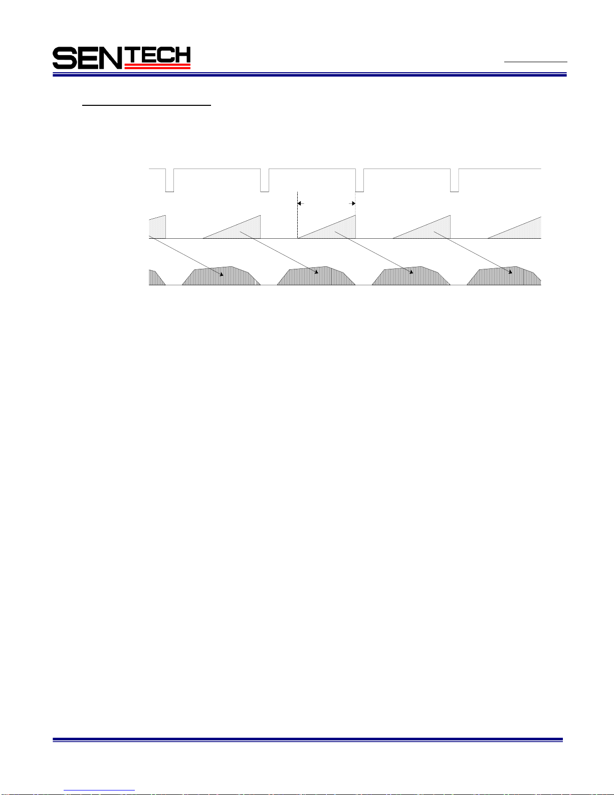
5 Camera function modes
5.1 Normal mode
E x p o s u r e
t i m e
I n t e r n a l V D
CCD
e x p o s u r e
V i d e o o u t
Page 37
No.11S098-03
37
STC-GE33OX/GEC33OX
Users guide Rev. 1.03
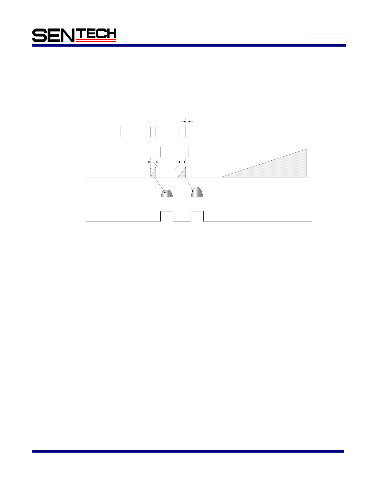
5.2 Pulse width trigger mode
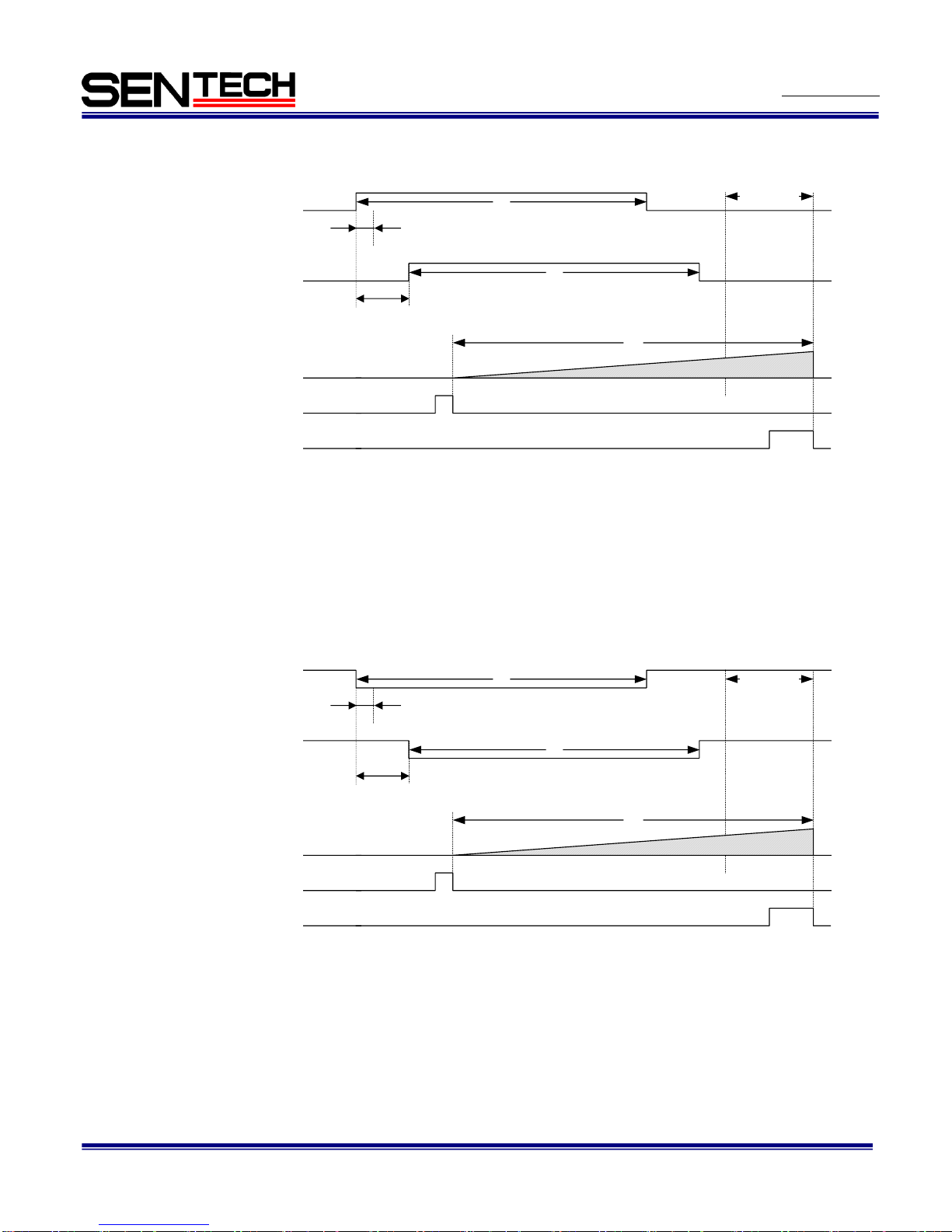
In this trigger mode with positive polarity, the camera exposure starts at the rising edge of the trigger pulse and
stops at the falling edge of the trigger pulse. Therefore, In the case of the exposure positive polarity is selected, the
exposure periods are the high states of the trigger pulse.
5.2.1 Timing
Note.1: The video output is going to be V reset by the next internal HD signal immediate after the exposure is
finished.
Note.2: The exposure time sets by the pulse width of the trigger signal.
Exposure
time
Max. 1H
Internal VD
CCD exposure
Trigger signal
(Positive)
Video out
*Note. 1
*Note. 2
FVAL
Page 38
No.11S098-03
38
STC-GE33OX/GEC33OX
Users guide Rev. 1.03
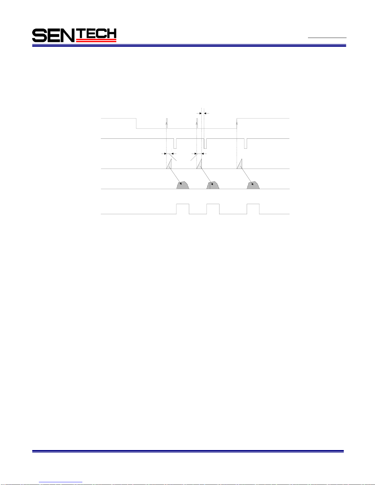
5.2.2 Exposure timing with the positive polarity trigger signal
Note.1: The trigger signal is removed by the filtering if the pulse width of the input trigger signal is less than 30
CLK.
Please input the trigger signal has more then 31 CLK pulse width.
Note.2: The exposure is going to start 75 CLK after the rising edge of the trigger signal.
5.2.3 Exposure timing with the negative polarity trigger signal
Note.1: The trigger signal is removed by the filtering if the pulse width of the input trigger signal is less than 30
CLK.
Please input the trigger signal has more then 31 CLK pulse width.
Note.2: The exposure is going to start 75 CLK after the rising edge of the trigger signal.
T1'
SUB
SG
(127 CLK)
Input Trigger signal
Exposure time
Exposure time: T1' = T1 + 127 CLK
T1
30 CLK
Filtering *Note.1
Trigger signal
(With Photocoupler delay)
T1
Less than
5 useconds
T1'
SUB
SG
(127 CLK)
Input Trigger signal
Exposure time
Exposure time: T1' = T1 + 127 CLK
T1
30 CLK
Filtering *Note.1
Trigger signal
(With Photocoupler delay)
T1
Less than
60 useconds
Page 39
No.11S098-03
39
STC-GE33OX/GEC33OX
Users guide Rev. 1.03
5.3 Edge preset trigger mode
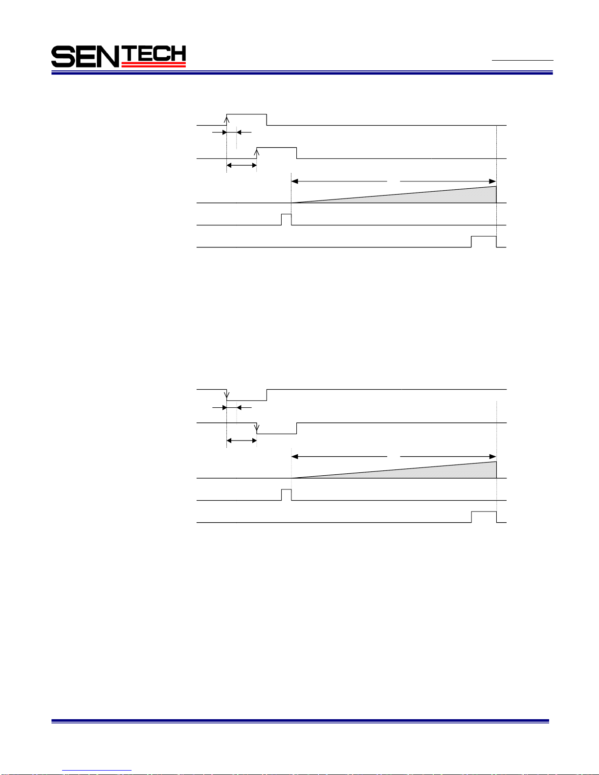
In this trigger mode, the camera exposure starts at the rising edge of the trigger pulse. Exposure duration time is
preset by the DIP Switch settings.
5.3.1 Timing
Note.1: The video output is going to be V reset by the next internal HD signal immediate after the exposure is
finished.
Note.2: The exposure time sets by the preset electronic shutter speed.
Exposure
time
Max. 1H
Internal VD
CCD exposure
Trigger signal
(Rising edge)
Video out
*Note. 1
*Note. 2
FVAL
Page 40
No.11S098-03
40
STC-GE33OX/GEC33OX
Users guide Rev. 1.03
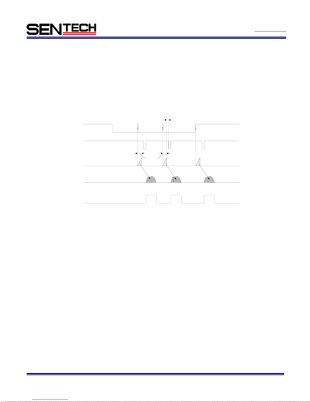
5.3.2 Exposure timing with the positive polarity trigger signal
Note.1: The trigger signal is removed by the filtering if the pulse width of the input trigger signal is less than 30
CLK
Please input the trigger signal has more then 31 CLK pulse width.
Note.2: The exposure is going to start 75 CLK after the rising edge of the trigger signal.
5.3.3 Exposure timing with the negative polarity trigger signal
Note.1: The trigger signal is removed by the filtering if the pulse width of the input trigger signal is less than 30
CLK
Please input the trigger signal has more then 31 CLK pulse width.
Note.2: The exposure is going to start 75 CLK after the rising edge of the trigger signal.
Input Trigger signal
Exposure time
T1'
SUB
SG
Exposure time: T1' = Preset exposure time
Filtering *Note.1
30CLK
Trigger signal
(With Photocoupler delay)
Less than
5 useconds
Input Trigger signal
Exposure time
T1'
SUB
SG
Exposure time: T1' = Preset exposure time
Filtering *Note.1
30CLK
Trigger signal
(With Photocoupler delay)
Less than
60 useconds
Page 41
No.11S098-03
41
STC-GE33OX/GEC33OX
Users guide Rev. 1.03
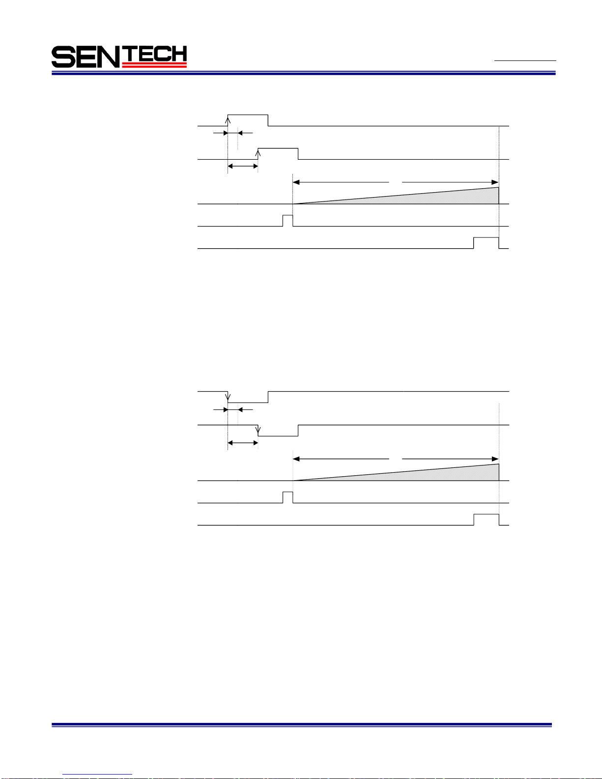
5.4 Edge preset trigger mode (The trigger input while the image is out)
In this trigger mode, the camera exposure starts at the rising edge of the trigger pulse. Exposure duration time is
preset by the DIP Switch settings.
It is necessary to disable the trigger signal mask with the communication when the trigger signal input is required
while the image is out.
It is necessary to set the “H reset” at the exposure start mode for do not generate the additional noise on the image
5.4.1 Timing
Note.1: The video output is going to be V reset by the next internal HD signal immediate after the exposure is
finished.
Note.2: The exposure time sets by the preset electronic shutter speed.
Exposure
time
Max. 1H
Internal VD
CCD exposure
Trigger signal
(Rising edge)
Video out
*Note. 1
*Note. 2
FVAL
Page 42
No.11S098-03
42
STC-GE33OX/GEC33OX
Users guide Rev. 1.03
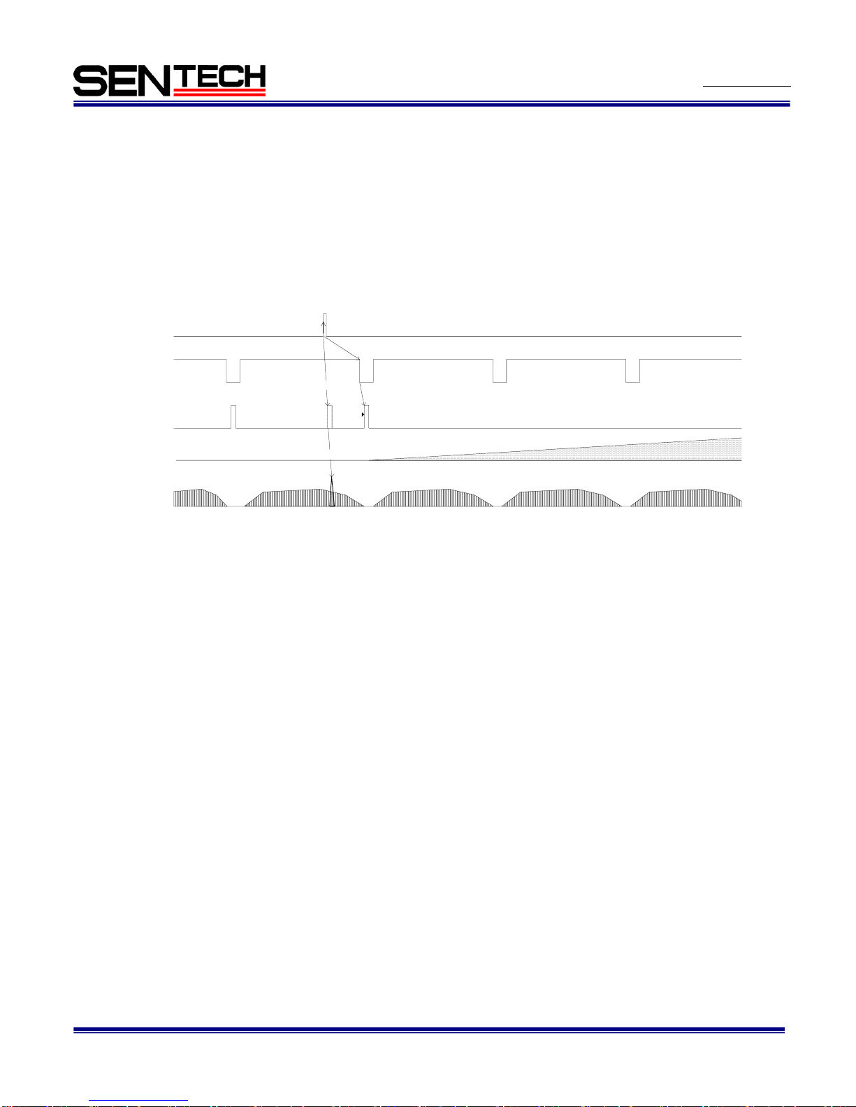
5.4.2 Exposure timing with the positive polarity trigger signal
Note.1: The trigger signal is removed by the filtering if the pulse width of the input trigger signal is less than 30
CLK
Please input the trigger signal has more then 31 CLK pulse width.
Note.2: The exposure is going to start 75 CLK after the rising edge of the trigger signal.
5.4.3 Exposure timing with the negative polarity trigger signal
Note.1: The trigger signal is removed by the filtering if the pulse width of the input trigger signal is less than 30
CLK
Please input the trigger signal has more then 31 CLK pulse width.
Note.2: The exposure is going to start 75 CLK after the rising edge of the trigger signal.
Input Trigger signal
Exposure time
T1'
SUB
SG
Exposure time: T1' = Preset exposure time
Filtering *Note.1
30CLK
Trigger signal
(With Photocoupler delay)
Less than
5 useconds
Input Trigger signal
Exposure time
T1'
SUB
SG
Exposure time: T1' = Preset exposure time
Filtering *Note.1
30CLK
Trigger signal
(With Photocoupler delay)
Less than
60 useconds
Page 43
No.11S098-03
43
STC-GE33OX/GEC33OX
Users guide Rev. 1.03
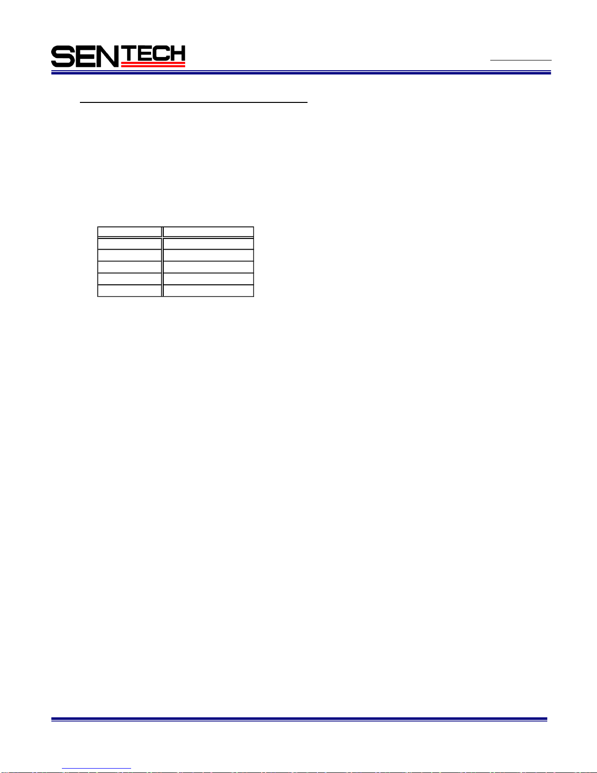
5.5 H reset mode
In this mode, the exposure can be start during the video is out from the camera without the horizontal noises.
Therefore, generates the SUB pulse to sweep the charges during the horizontal blanking to prevent from getting
horizontal noises.
The image is getting the horizontal noises caused by generates the SUB pulse during the video out in normal mode,
which is this mode is OFF.
The maximum delay to start exposure from the trigger input is 1H.
Next HD
Video out
SUB pulse
Internal HD
CCD exposure
Trigger signal
(Rising edge)
Noise
Normal SUB pulse timing
Page 44
No.11S098-03
44
STC-GE33OX/GEC33OX
Users guide Rev. 1.03
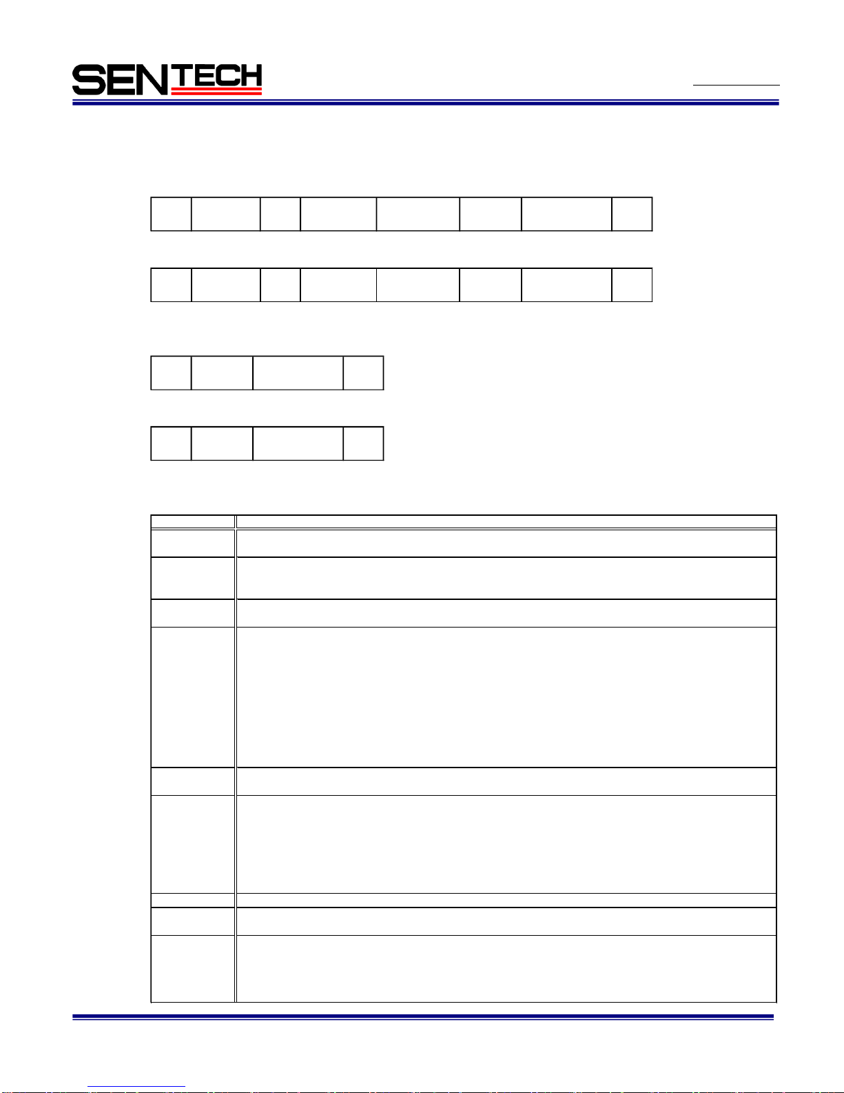
6 The communication protocol specifications
This camera has the communication function that enables external devises like PC control the camera functions.
Please use “StCamGigEWare” or “StGigECtrl” communication software or use following the communication
protocol to communicate to the camera.
6.1 The communication method
UART (RS232C), Binary communication
6.2 The communication settings
Settings
Baud rate 115,200bps
Data bit 8bit
Parity None
Stop bit 1bit
Flow control None
Page 45
No.11S098-03
45
STC-GE33OX/GEC33OX
Users guide Rev. 1.03
6.3 The communication format
A. The sending data format from the PC to the camera is as follows:
a. Send the read command
b. Send the write command
B. The receiving data format from the camera is as follows:
a. After sent the read command
b. After sent the write command
C. Descriptions of the format
SOF Data length Data EOF
(8bit) (8bit) (Data length byte) (8bit)
SOF Device code Read Page selection Command code Data length Data EOF
(8bit) (6bit) (1bit) (1bit) (8bit) (8bit) (Dummy, 1byte) (8bit)
Name
SOF
Device code
Read / Write
Page selection
Command
code
Data length
Data
The data length is depending on the command when send write command.
The value of the data is depending on the command
Sets (or gets) the value is as “03H” always
End of the frame
Result of the sending command
EOF
Receiving code
Please check from the following page.
Data length (Unit: byte)
The data length is depending on the command after sent read command.
Receiving data
The data length is “00H” after sent write command.
Sending data
The data length is 1 byte when send read command.
The data of the EEPROM is replaced by sent data when sent write command.
The camera sends the receiving coce as "01H" to the PC after the data of the EEPROM is replaced.
Sets (or gets) the value is as “02H” always.
Sets (or gets) “1” when send write command.
Sets “0” when access to the command register of the camera
The data of the command register is replaced by the sent data when sent write command.
The data of the EEPROM is not replaced.
Sets “1” when access to the EEPROM of the camera
The camera works with the data of the EEPROM when the power on the camera.
Gets the data from the EEPROM when sent read.
Start of the frame
Descriptions
Sets "000000" when access to the camera function setting.
Sets (or gets) “0” when send read command.
Gets current data from the command register when sent read command.
Sets "100000" when access to the camera extend function setting.
Please check the "The camera commands list" and "Description of the camera control commands"
SOF Device code Write Page selection Command code Data length Data EOF
(8bit) (6bit) (1bit) (1bit) (8bit) (8bit) (Data length byte) (8bit)
SOF Data length Receiving code EOF
(8bit) (8bit) "00" (8bit) (8bit)
01H: OK (ACK), 14H: Time out error (Two seconds),
16H: Data length error (Not mach), 17H: EPPROM write error
Page 46

No.11S098-03
46
STC-GE33OX/GEC33OX
Users guide Rev. 1.03
D. Example command
Send the read command to read the 00H address data of the register
02, 00, 00, 01, 00, 03
SOF, (Device code/Read/Register), Command code, Data length, Data, EOF
The return command
02, 01, 00, 03
Page 47
No.11S098-03
47
STC-GE33OX/GEC33OX
Users guide Rev. 1.03
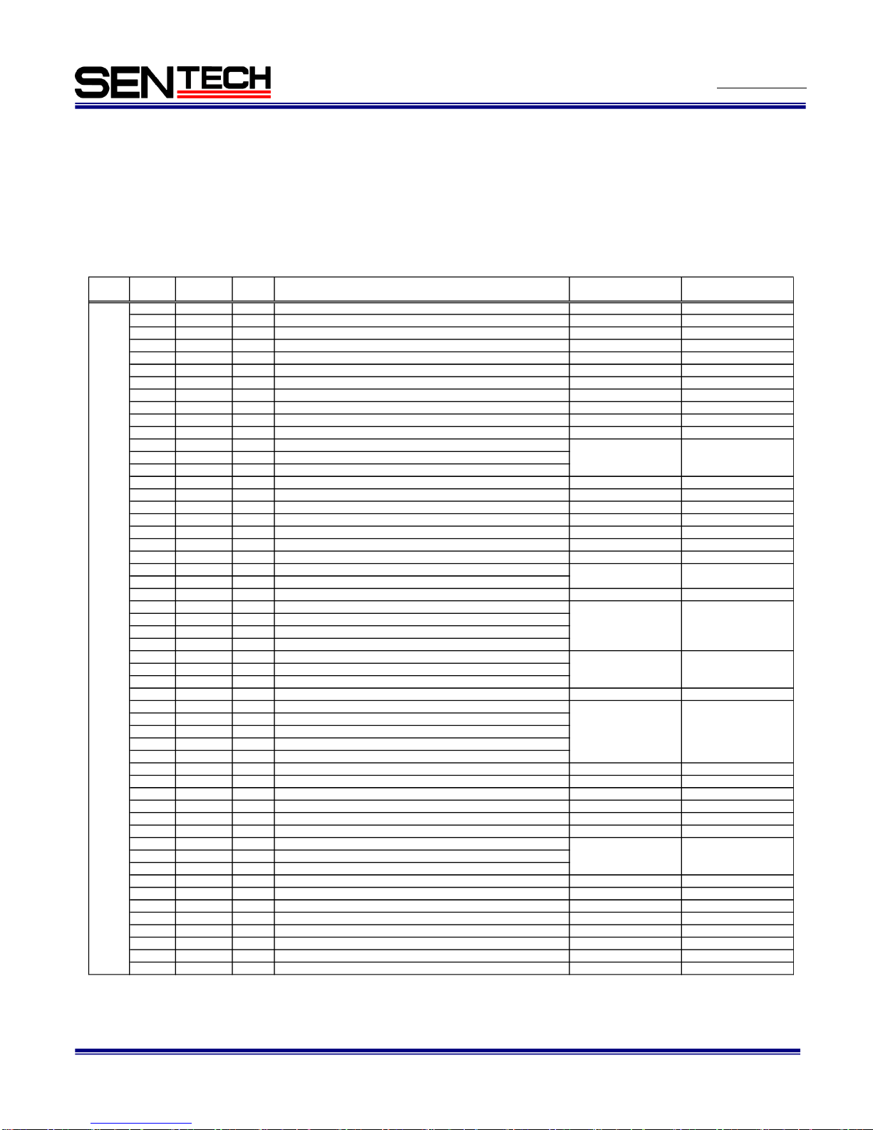
6.4 The camera control commands
6.4.1 The camera control commands list
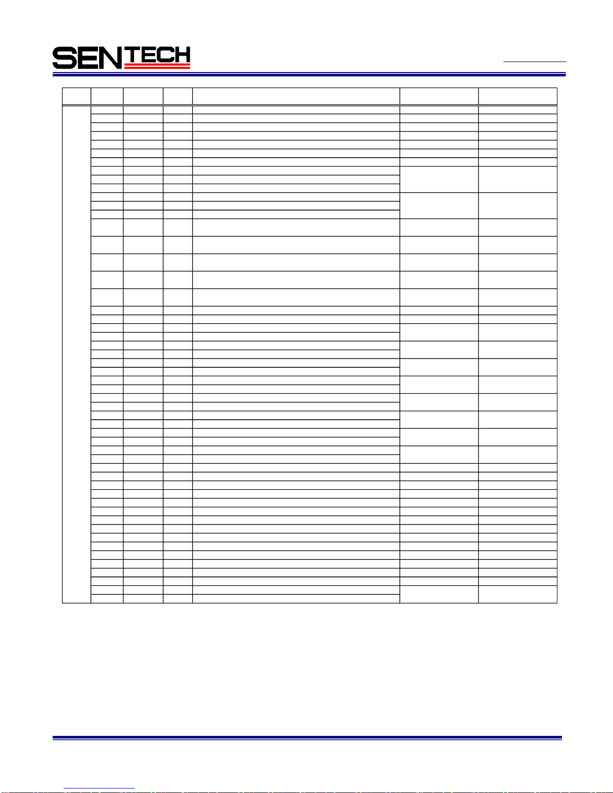
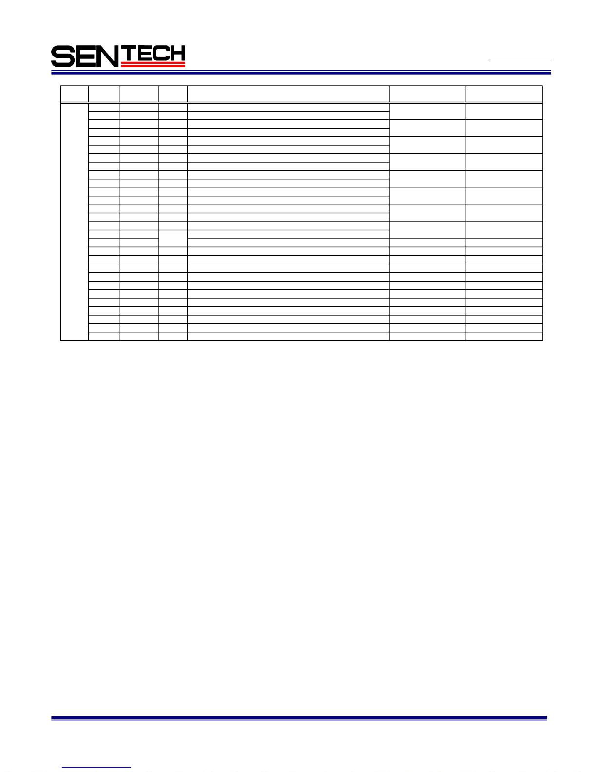
Note. 1: The data unit of the each command is 1byte (8bit).
Note. 2: The data can be saved to the EEPROM if “x” in the “Save to EEPROM” column in the list.
Note. 3: The camera is operating with the data of the EEPROM when the power on the camera.
Read / Write
00 to 0FH Reserved
10H Read / Write x The camera function mode 1 (8bit: D[7..0])
11H Read / Write x The camera function mode 2 (8bit: D[7..0])
12H Read / Write x The camera function mode 3 (8bit: D[7..0])
13H Read / Write x The camera function mode 4 (8bit: D[7..0])
14 to15H Reserved
16H Read / Write x Software trigger mode (8bit: D[7..0])
17H Read / Write x Image data reset (8bit: D[7..0])
18H Reserved
19H Read / Write x Image output formant (8bit: D[7..0])
1A to1FH Reserved
20H Read / Write x The exposure time (useconds) of the electronic shutter (24bit: D[7..0])
21H Read / Write x The exposure time (useconds) of the electronic shutter (24bit: D[15..8])
22H Read / Write x The exposure time (useconds) of the electronic shutter (24bit: D[24..16])
23 - 2FH Reserved
30H Read / Write x CDS gin (8bit: D[7..0])
31H Read / Write x The digital gain (8bit: D[7..0])
32H Read / Write x The gain offset (8bit: D[7..0])
33 to 37H Reserved
38H Read / Write x The clamp level (8bit: D[7..0])
39 to 3DH Reserved
3EH Read / Write x White clip for the test pattern (16bit: D[15..8])
3FH Read / Write x White clip for the test pattern (16bit: D[7..0])
40 to 4FH Reserved
50H Read / Write x The trigger delay time (useconds) (Integer) (24bit: D[7..0])
51H Read / Write x The trigger delay time (useconds) (Integer) (24bit: D[15..8])
52H Read / Write x The trigger delay time (useconds) (Integer) (24bit: D[23..16])
53H Read / Write x The trigger delay time (useconds) (Decimal) (8bit: D[7..0])
54H Read / Write x The strobe signal delay time (useconds) (Integer) (24bit: D[7..0])
55H Read / Write x The strobe signal delay time (useconds) (Integer) (24bit: D[15..8])
56H Read / Write x The strobe signal delay time (useconds) (Integer) (24bit: D[23..16])
57H Read / Write x The strobe signal delay time (useconds) (Decimal) (8bit: D[7..0])
58H Read / Write x Frame rate (Hz) (Integer) (16bit: D[7..0])
59H Read / Write x Frame rate (Hz) (Integer) (16bit: D[15..8])
5AH Read / Write x Frame rate (Hz) (Decimal) (24bit: D[7..0])
5BH Read / Write x Frame rate (Hz) (Decimal) (24bit: D[15..8])
5CH Read / Write x Frame rate (Hz) (Decimal) (24bit: D[23..16])
5D to 77H Reserved
78H Read / Write x Test pattern selection (8bit: D[7..0])
79H Read / Write x Image effect selection (8bit: D[7..0])
7A to 7FH Reserved
80H Read / Write EEPROM control (8bit: D[7..0])
81 to 8FH Reserved
90H Read / Write x The strobe signal delay time (useconds) (Integer) (24bit: D[7..0])
91H Read / Write x The strobe signal delay time (useconds) (Integer) (24bit: D[15..8])
92H Read / Write x The strobe signal delay time (useconds) (Integer) (24bit: D[23..16])
93H Read / Write x The strobe signal delay time (useconds) (Decimal) (8bit: D[7..0])
94 to EFH Reserved
F0H Read / Write x The signals of the power/IO connector (8bit: D[7..0])
F1H Read / Write x UserOutput signal for the power/IO connector (8bit: D[7..0])
F2 to F7H Reserved
F8H Read / Write x The signals of the power/IO connector (8bit: D[7..0])
F9H Read / Write x The signals of the power/IO connector (8bit: D[7..0])
FA to FFH Reserved
-
-
0
0 to 2,000,000
0
0 to 99
0
0 to 2,000,000
9
0 to 31
1,023
0 to 4,095
-
00H
-
-
---
00H
00H
-
0
0 to 2,000,000
Device
Code
000000
Save to
EEPROM
-
60H
-
00H
0
0FH0-
00H
The factory adjusted value
-
0 to 99
00H
Function
Command
No.
-
89H
Data range
Initial data
-
The factory adjusted value
-
0
0 to 255
0 to 16,777,215
00H
00H
-
-
-
-
20H
00H
00H
-
89.91172
0.72028 to 360.33325
-
-
-
-
-
-
-
Page 48
No.11S098-03
48
STC-GE33OX/GEC33OX
Users guide Rev. 1.03
Read / Write
00 to 17H Reserved
18H Read / Write x JTAG for User configurable FPGA (8bit: D[7..0])
19H Read / Write User configurable FPGA Enable (8bit: D[7..0])
1A to 1FH Reserved
20H Read / Write x Exposure mode (8bit: D[7..0])
21H Read / Write x AGC maximum limit (8bit: D[7..0])
22H Reserved
23H Read / Write x The upper limit of the electronic shutter for auto shutter (20bit: D[7..0])
24H Read / Write x The upper limit of the electronic shutter for auto shutter (20bit: D[15..8])
25H Read / Write x The upper limit of the electronic shutter for auto shutter (20bit: D[20..16])
26H Read / Write x The lower limit of the electronic shutter for auto shutter (20bit: D[7..0])
27H Read / Write x The lower limit of the electronic shutter for auto shutter (20bit: D[15..8])
28H Read / Write x The lower limit of the electronic shutter for auto shutter (20bit: D[20..16])
29H Read / Write x Weight1 for ALC (8bit: D[7..0]) D3 to D0: 0 to 15
D7 to D4: 0 to 15
2AH Read / Write x Weight2 for ALC (8bit: D[7..0]) D3 to D0: 0 to 15
D7 to D4: 0 to 15
2BH Read / Write x Weight3 for ALC (8bit: D[7..0]) D3 to D0: 0 to 15
D7 to D4: 0 to 15
2CH Read / Write x Weight4 for ALC (8bit: D[7..0]) D3 to D0: 0 to 15
D7 to D4: 0 to 15
2DH Read / Write x Weight5 for ALC (8bit: D[7..0]) D3 to D0: 0 to 15
D7 to D4: 0
2EH Read / Write x Target brightness for ALC (8bit: D[7..0])
2FH Read / Write x ALC peak-average (8bit: D[7..0])
30H Read / Write x Vertical_1 position for the ALC weight area (16bit: D[7..0])
31H Read / Write x Vertical_1 position for the ALC weight area (16bit: D[15..8])
32H Read / Write x Vertical_2 position for the ALC weight area (16bit: D[7..0])
33H Read / Write x Vertical_2 position for the ALC weight area (16bit: D[15..8])
34H Read / Write x Vertical_3 position for the ALC weight area (16bit: D[7..0])
35H Read / Write x Vertical_3 position for the ALC weight area (16bit: D[15..8])
36H Read / Write x Vertical_4 position for the ALC weight area (16bit: D[7..0])
37H Read / Write x Vertical_4 position for the ALC weight area (16bit: D[15..8])
38H Read / Write x Horizontal_1 position for the ALC weight area (16bit: D[7..0])
39H Read / Write x Horizontal_1 position for the ALC weight area (16bit: D[15..8])
3AH Read / Write x Horizontal_2 position for the ALC weight area (16bit: D[7..0])
3BH Read / Write x Horizontal_2 position for the ALC weight area (16bit: D[15..8])
3CH Read / Write x Horizontal_3 position for the ALC weight area (16bit: D[7..0])
3DH Read / Write x Horizontal_3 position for the ALC weight area (16bit: D[15..8])
3EH Read / Write x Horizontal_4 position for the ALC weight area (16bit: D[7..0])
3FH Read / Write x Horizontal_4 position for the ALC weight area (16bit: D[15..8])
40H Read / Write x White balance mode (8bit: D[7..0])
41H Read / Write x Preset_1 white balance (Red gain) (8bit: D[7..0])
42H Read / Write x Preset_1 white balance (Gr gain) (8bit: D[7..0])
43H Read / Write x Preset_1 white balance (Blue gain) (8bit: D[7..0])
44H Read / Write x Preset_1 white balance (Gb gain) (8bit: D[7..0])
45H Read / Write x Preset_2 white balance (Red gain) (8bit: D[7..0])
46H Read / Write x Preset_2 white balance (Gr gain) (8bit: D[7..0])
47H Read / Write x Preset_2 white balance (Blue gain) (8bit: D[7..0])
48H Read / Write x Preset_2 white balance (Gb gain) (8bit: D[7..0])
49H Read / Write x Preset_3 white balance (Red gain) (8bit: D[7..0])
4AH Read / Write x Preset_3 white balance (Gr gain) (8bit: D[7..0])
4BH Read / Write x Preset_3 white balance (Blue gain) (8bit: D[7..0])
4CH Read / Write x Preset_3 white balance (Gb gain) (8bit: D[7..0])
4DH Reserved
4EH Read / Write x Threshold for auto white balance (16bit: D[7..0])
4FH Read / Write x Threshold for auto white balance (16bit: D[16..8])
-
-
3,072
0 to 4,095
0
0 to 255
0
0 to 255
0
0 to 255
0
0 to 255
0
0 to 255
0
0 to 255
0 to 255
0
0 to 255
0
0 to 255
0
00H
0
0 to 255
0
0 to 255
0
0 to 255
Device
Code
Save to
EEPROM
-
-
255
100000
0
Function
Command
No.
196
Data range
Initial data
0 to 255
0 to 255
01H
0 to 255
1AH
11H
-
128
0 to 1,048,575
11H
11H
-
00H
0
0 to 1,048,575
11,122
00H
00H
0 to 647
36
0 to 493
0 to 493
0 to 493
298
32
-
-
612
0 to 647
252
0 to 647
396
0 to 647
0 to 493
462
Page 49
No.11S098-03
49
STC-GE33OX/GEC33OX
Users guide Rev. 1.03
Read / Write
50H Read / Write x Y_offset for AOI (8bit: D[7..0])
51H Read / Write x Y_offset for AOI (16bit: D[15..8])
52H Read / Write x Height for AOI (8bit: D[7..0])
53H Read / Write x Height for AOI (16bit: D[15..8])
54H Read / Write x X_offset for AOI (8bit: D[7..0])
55H Read / Write x X_offset for AOI (16bit: D[15..8])
56H Read / Write x Width for AOI (8bit: D[7..0])
57H Read / Write x Width for AOI (16bit: D[15..8])
58H Read / Write x Vertical_1 position for the white balance area (16bit: D[7..0])
59H Read / Write x Vertical_1 position for the white balance area (16bit: D[15..8])
5AH Read / Write x Vertical_2 position for the white balance area (16bit: D[7..0])
5BH Read / Write x Vertical_2 position for the white balance area (16bit: D[15..8])
5CH Read / Write x Horizontal_1 position for the white balance area (16bit: D[7..0])
5DH Read / Write x Horizontal_1 position for the white balance area (16bit: D[15..8])
5EH Read / Write x Horizontal_2 position for the white balance area (16bit: D[7..0])
5FH Read / Write x Horizontal_2 position for the white balance area (16bit: D[15..8])
60H Read / Write x Camera mode1 (8bit: D[7..0])
61 to 7FH Reserved
80H Read / Write x Push set white balance (Red gain) (8bit: D[7..0])
81H Read / Write x Push set white balance (Gr gain) (8bit: D[7..0])
82H Read / Write x Push set white balance (Blue gain) (8bit: D[7..0])
83H Read / Write x Push set white balance (Gb gain) (8bit: D[7..0])
84 to 91H Reserved
92H Read / Write x Iris lens manual adjustment (8bit: D[7..0])
93 to BFH Reserved
C0H Read / Write x Image data between FPGAs (8bit: D[7..0])
C1H Read / Write x Output signal selection (8bit: D[7..0])
C2 toFFH Reserved
-
-
-
00H
00H
-
8 <= X <= 648
X: X_offset + width
648
8 <= X <= 648
X: X_offset + width
Y: Y_offset + Height
494
2 <= Y <= 494
Y: Y_offset + Height
Device
Code
Save to
EEPROM
0
Command
No.
-
493
647
0
0
100000
Function
Data range
Initial data
0
0 to 255
00H
0 to 255
0
2 <= Y <= 494
0
0 to 255
01H
-
0
0
-
-
0 to 493
0 to 493
0 to 647
0 to 647
0 to 255
Page 50
No.11S098-03
50
STC-GE33OX/GEC33OX
Users guide Rev. 1.03
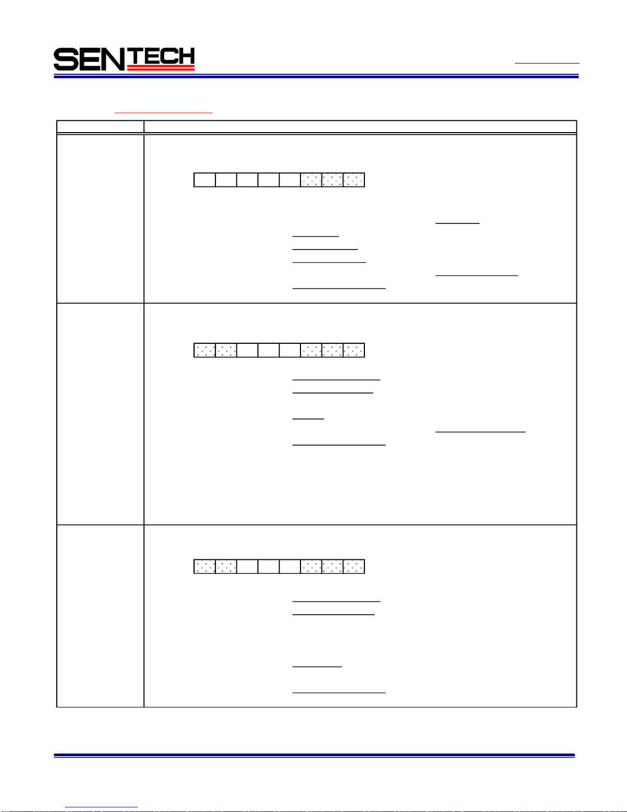
6.4.2 Description of the camera control commands (Device code: 000000)
(The under line settings are the factory default settings)
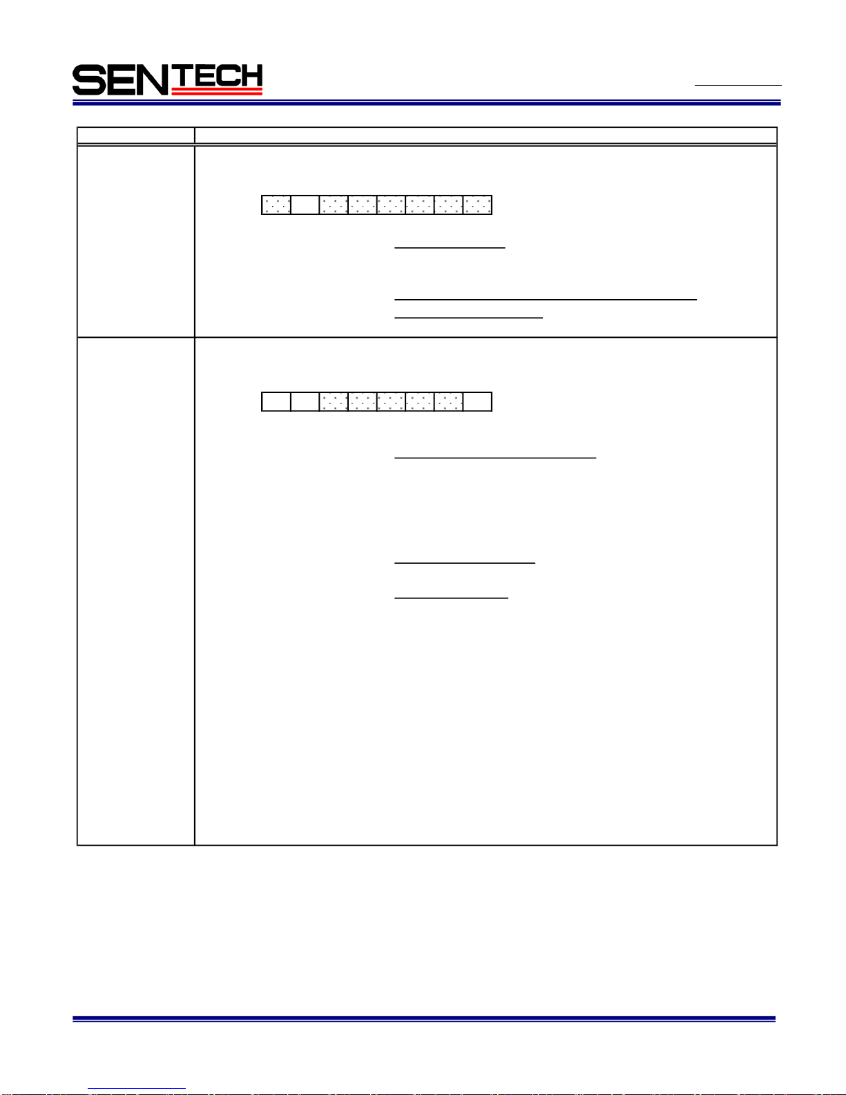
Command No.
10H:
MOD1[7..0]
D7: Continuous / Trigger mode
0: Auto, 1: Manual
D6: Trigger polarity
0: Positive, 1: Negative
D5: Trigger mode
0: Edge preset, 1: Pulse width
D4: Binning mode
0: OFF (Normal), 1: ON (Binning)
D3: Scanning mode 0: Full scanning, 1: Partial scanning
D2 to D0: No function Sets always as "001"
11H:
MOD2[7..0]
D7 to D6: No function Sets always as "00"
D5: TG reset
0: TG pertial reset, 1: TG pertial reset OFF
D4: Smear half reduction
0: OFF, 1: ON
D3: Function mode 0: Trigger mode, 1: Continuous mode
D2 to D0: No function Sets always as "111"
as manual.
12H:
MOD3[7..0]
D7 to D6: No function Sets always as "00"
D5: Trigger signal type
0: Software trigger,
1: Hardware triger
D4 to D3: Exposure start mode
00: Normal, 10 to 11: H reset,
D2 to D0: No function Sets always as "000"
Sets the camera function mode.
D[7..0]
Note.1: Function mode is enable when the "Continuous / Trigger mode (MOD1-D7)" is
Note.2: No video output without the trigger signal input while the camera works with
[The camera function mode 3] Initial data: 00H
the trigger mode.
01: No function (Prohibited setting. Do not set this value)
D[7..0]
(Trigger signal input from 5pin of Power/IO connector)
Command descriptions
[The camera function mode 2] Initial data: 0FH
[The camera function mode 1] Initial data: 89H
Sets the camera function mode.
D[7..0]
Sets the camera function mode.
D7 D6 D5 D4 D3 D2 D1 D0
D7 D6 D5 D4 D3 D2 D1 D0
D7 D6 D5 D4 D3 D2 D1 D0
Page 51
No.11S098-03
51
STC-GE33OX/GEC33OX
Users guide Rev. 1.03
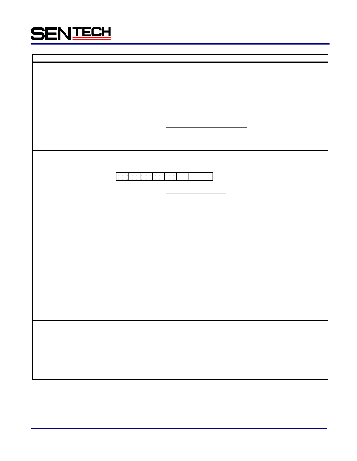
Command No.
13H:
MOD4[7..0]
D7: No function Sets always as "0"
D6: Trigger signal mask while image out
0: OFF,
D5 to D0: No function Sets always as "100000"
16H:
SOFTRG[7..0]
D7 to D6: Software trigger source selection
00: Programming software trigger,
10: Command software trigger,
(200 useconds pulse width trigger signal)
11: No function
(Prohibited setting. Do not set this value)
D5 to D1: No function Sets always as "00000"
D0: Generate command software trigger
0: Hold (Low state),
1: Generate command software trigger
(200 useconds high state)
Note.4: When select "Command software trigger", it's necessary to generate software
trigger signal with "Generate command software trigger(SOFTRIG-D0)".
Note. 3: When use "User configurable FPGA generates trigger",
Please generate the trigger signal has more than 200 useconds pulse duration
in the user configurable FPGA.
Command descriptions
[The camera function mode 4] Initial data: 60H
[Software trigger setting] Initial data: 00H
Sets the camera function mode.
D[7..0]
1: ON (Invalid the trigger signal while image is out)
Sets the source of the softwre trigger.
D[7..0]
Note.1: The software trigger source selection is enable when
01: User configurable FPGA generates trigger,
when "Trigger signal type (MOD3-D5)" is the software trigger (sets as 0).
Note. 2: When use "Programming software trigger",
Please make the program for set up the pulse duration, the trigger signal interval and
the generate the trigger signal with the "StGigE SDK".
D7 D6 D5 D4 D3 D2 D1 D0
D7 D6 D5 D4 D3 D2 D1 D0
Page 52
No.11S098-03
52
STC-GE33OX/GEC33OX
Users guide Rev. 1.03
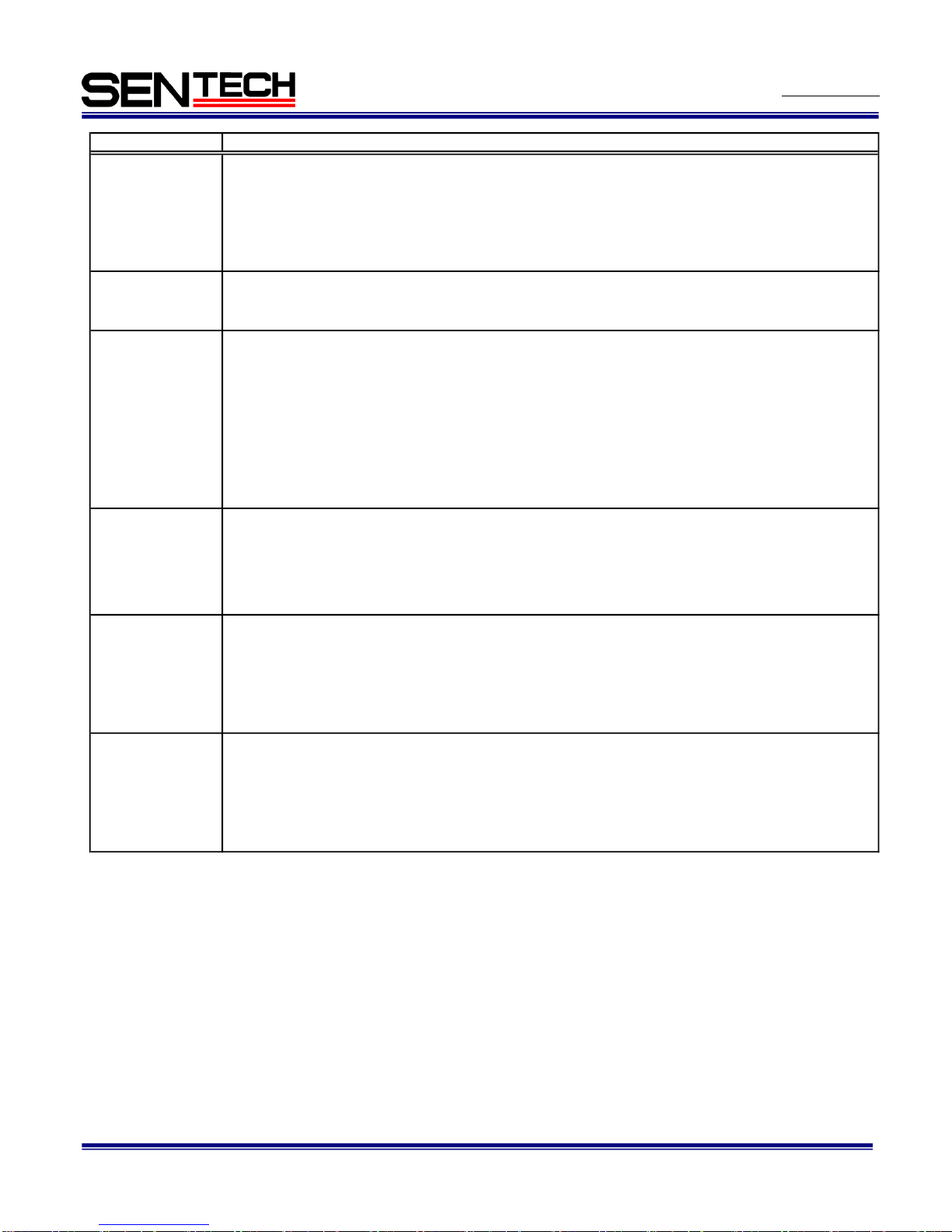
Command No.
17H:
IMAGEREST
[7..0]
D7 to D1: No function Sets always as "0000000"
D0: Image data reset
0: FVAL/LVAL/Image data reset,
(FVAL, LVAL and the image data are low state data),
1: FVAL/LVAL/Image data out
19H:
FORMATE
[7..0]
D7 to D3: No function Sets always as "00000"
D2 to D0:
20H: EXPTM
[7..0]
21H: EXPTM
[15..8]
22H: EXPTM
[23..16]
30H:
PGA[7..0]
D[7..0]
[Image data reset] Initial data: 00H
Reset the Image data (FVAL, LVAL and the image data).
Change from the reset to the image data out after start the image acquistion.
The image data is not output when reset the image data.
* CDS_BASEGAIN[15..0]:
The gain base offset (The value of the address 5EH and 5FH)
* GOFS[7..0]:
Command descriptions
[The exposure time (useconds) of the electronic shutter]
[CDS gain] Initial data: PGA[7..0] = 0, data range:0 to 255
Initial data: EXPTM[23..0] = 0, data range: 0 to 16,777,215
Sets the exposure time for electronic shutter.
Exposure time = EXPTM[23..0] useconds
When sets as 0, the electronic shutter is OFF.
The gain offset (The value of the address 32H)
Sets the CDS gain (programable gain).
CDS gain = 6.16 + 0.04 x (PGA[7..0] X 2 + GOFS[7..0]) dB
[Image output format] Initial data: 00H
Sets the image output format.
D[7..0]
Image output format
000: Mono8 (Monochrome) / BayerRG8 (Color),
001: Mono10 (Monochrome) / BayerRG10 (Color),
010: Mono10Packed (Monochrome) / BayerRG12 (Color),
011: Mono12 (Monochrome) / BayerRG10Packed (Color),
100: Mono12Packed (Monochrome) / BayerRG12Packed (Color),
101: No function (Monochrome) / RGB8Packed (Color),
110 to 111: No function (Prohibited setting. Do not set this value)
D7 D6 D5 D4 D3 D2 D1 D0
Page 53
No.11S098-03
53
STC-GE33OX/GEC33OX
Users guide Rev. 1.03
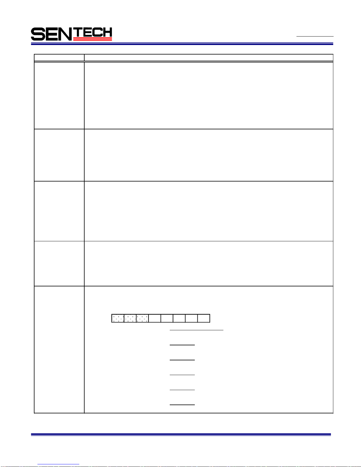
Command No.
31H:
DGB[7..0]
32H:
GOFS[7..0]
38H:
CLAMP[7..0]
3EH:
WHITE_CLIP
[15..8]
3FH:
WHITE_CLIP
[7..0]
50H:DELAY_I
[7..0]
51H: DELAY_I
[15..8]
52H: DELAY_I
[23..16]
53H:DELAY_F
[7..0]
Sets the white clip level for the white clip test pattern.
Delay time for the trigger signal = (DELAY_I[23..0]). (DELAY_F[7..0]) useconds
Command descriptions
[The delay time (usecond, integer) for the trigger signal]
Initial data: DELAY_I[23..0] = 0, data range: 0 to 2,000,000
Sets the delay time that is from the trigger signal input to start exposure as usecond.
[The white clip level for the white clip test pattern
Initial data: WHITE_CLIP[15..0] = 1,023, data range: 0 to 4,095
Initial data: DELAY_F[23..0] = 0, data range: 0 to 99
[The delay time (usecond, decimal) for the trigger signal]
Sets the delay time that is from the trigger signal input to start exposure as usecond.
Delay time for the trigger signal = (DELAY_I[23..0]). (DELAY_F[7..0]) useconds
[The digital gain] Initial data: DGB[7..0] = The factory adjusted value
Video level = (Input video level - CLAMP level ) x (1 + DGB[7..0] / 128) + CLAMP Level
* CLAMP Level
Clamp level (The calculated value of the address 38H)
Clamp level = (CLAMP[7..0] X 8 + 56) / 16 (for 8bit output)
[The gain offset]
[The clamp level] Initial data: CLAMP[7..0] = 9, data range: 0 to 31
Sets the clamp level (The clamp level of the black signal).
Automaticaly sets 31 when sets more then 31.
Initial data: GOFS[7..0] = The factory adjusted value, data range: 0 to 255
Clamp level = CLAMP[7..0] X 8 + 56 (for 12bit output)
Clamp level = (CLAMP[7..0] X 8 + 56) / 4 (for 10bit output)
Page 54
No.11S098-03
54
STC-GE33OX/GEC33OX
Users guide Rev. 1.03
Command No.
54H:
STROBEDELAY_I
[7..0]
55H:
STROBEDELAY_I
[15..8]
56H:
STROBEDELAY_I
[23..16]
57H:
STROBEDELAY_F
Initial data: STROBEDELAY_F[23..0] = 0, data range: 0 to 99
[7..0] Sets the delay time that is from the trigger signal input to the strobe signal output
(STROBEDELAY_I[23..0]). (STROBEDELAY_F[7..0]) useconds
58H:FPS_I
[7..0]
59H: FPS_I
[15..8]
0.72028 to 360.33325 Hz
89.91172 Hz (as initial data)
5AH:FPS_F
[7..0]
5BH:FPS_F
[15..8]
5CH:FPS_F
[23..16]
5DH:
IOSIGNAL_POL
[7..0]
D7 to D5: No function Sets always as "000"
D4:
0: Normal, 1: Reverse
D3:
0: Normal, 1: Reverse
D2:
0: Normal, 1: Reverse
D1:
0: Normal, 1: Reverse
D0:
0: Normal, 1: Reverse
[Frame rate (Hz, integer)] Initial data: FPS_F[15..0] = 89, data range: 0 to 360
Sets the frame rate as Hz.
Frame rate = (FPS_I[15..0]). (FPS_F[23..0]) Hz
Frame rate = (FPS_I[15..0]). (FPS_F[23..0]) Hz
Frame rate range:
Max frame rate for full resolution
D[7..0]
The polarity of the output signal for 4 pin of the power/IO connector
The polarity of the output signal for 3 pin of the power/IO connector
The polarity of the output signal for 6 pin of the power/IO connector
The polarity of the output signal for 5 pin of the power/IO connector
The polarity of the output signal for 7 pin of the power/IO connector
Command descriptions
[The delay time (usecond, integer) for the strobe signal]
Sets the delay time that is from the trigger signal input to the strobe signal output as usecond.
Delay time for the strobe signal =
(STROBEDELAY_I[23..0]). (STROBEDELAY_F[7..0]) useconds
Initial data: STROBEDELAY_I[23..0] = 0, data range: 0 to 2,000,000
[The delay time (usecond, decimal) for the trigger signal]
[IO signal polarity] Initial data: IOSIGNAL_POL[7..0] = 00H
Sets the polarity of the IO signals.
Delay time for the strobe signal =
[Frame rate (Hz, decimal)]
Initial data: FPS_F[23..0] = 91,172, FPS_I[15..0], data range: 0 to 99,999
Sets the frame rate as Hz.
D7 D6 D5 D4 D3 D2 D1 D0
Page 55
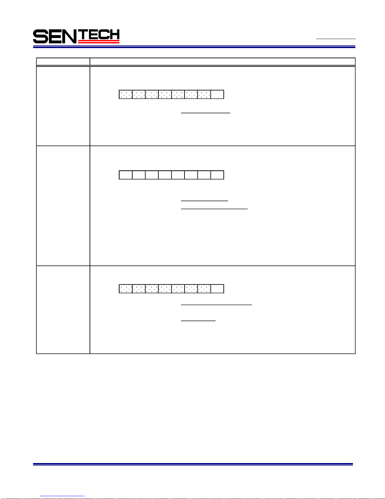
No.11S098-03
55
STC-GE33OX/GEC33OX
Users guide Rev. 1.03
Command No.
78H:
TESTP[7..0]
00H: Video output, 01H: Gray schale,
02H: Ramp wave, 03H: 100% White,
04H: White clip, 05H: Color bar (RGB bayer),
Others: Black
79H:
EFFCT[7..0]
D7:
0: Positive image, 1: Negative image
D6 to D0: Image effect
00H: No effect (Original), 01H: 9bit gradation,
02H: 8bit gradation, 03H: 7bit gradation,
04H: 6bit gradation, 05H: 5bit gradation,
06H: 4bit gradation, 07H: 3bit gradation,
08H: 2bit gradation, 09H: 1bit gradation,
0A to 7FH: No function
(Prohibited setting. Do not set these values)
80H:
E2P[7..0]
D[7..0]
D7 to D1: No function Sets always as "0000000"
D0: Write control to the EEPROM
0: Prohibited, 1: Accept
Sets the test pattern output form the camera.
D[7..0]
[Test pattern selection] Initial data: TESTP[7..0] = 00H
[EEPROM control] Initial data: E2P[7..0] = 00H
Command descriptions
[Image effect selection] Initial data: EFFCT[7..0] = 00H
Note. This bit is cleared to "0" automatically by the internal process after the execution
of the command.
Sets the imgae effect.
D[7..0]
Negative video / Positive video selection
D7 D6 D5 D4 D3 D2 D1 D0
D7 D6 D5 D4 D3 D2 D1 D0
D7 D6 D5 D4 D3 D2 D1 D0
Page 56
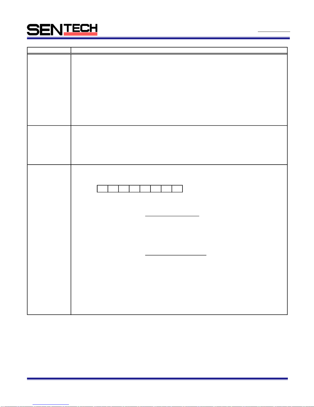
No.11S098-03
56
STC-GE33OX/GEC33OX
Users guide Rev. 1.03
Command No.
90H:
STROBEON_I
[7..0]
91H:
STROBEON_I
[15..8]
92H:
STROBEON_I
0: No strobe signal output
[23..16]
1 to 9: Active time is 10 useconds
More than 10 Active time is as set time
93H:
STROBEON_F
Initial data: STROBEDELAY_F[23..0] = 0, data range: 0 to 99
[7..0]
F0H:
OUTSEL[7..0]
D7 to D4:
0: FrameTriggerWait signal, 1: UserOutput signal,
2: ExposureActive signal, 3: TriggerAuxiliary signal,
5: SensorReadOut signal, 6: StrobeSignal signal,
7 to F: No function
D3 to D0:
0: FrameTriggerWait signal, 1: UserOutput signal,
2: ExposureActive signal, 3: TriggerAuxiliary signal,
5: SensorReadOut signal, 6: StrobeSignal signal,
7 to F: No function
Command descriptions
[The output signal selection for the power/IO connector] Initial data: OUTSEL[7..0] = 20H
Sets the output signal from the power/IO connector.
Sets the active time for the strobe signal as usecond.
Active time for the strobe signal = (STROBEON_I[23..0]). (STROBEON_F[7..0]) useconds
[The strobe signal active time (usecond, integer)]
Initial data: STROBEDELAY_I[23..0] = 0, data range: 0 to 2,000,000
Sets the active time for the strobe signal as usecond.
Active time for the strobe signal = (STROBEON_I[23..0]). (STROBEON_F[7..0]) useconds
(Prohibited setting. Do not set this value)
Output signal for 3 pin of the power/IO connector
"UserOutput signal for the power/IO connector(TEST2-D3,4)".
Note: When select "UserOutput signal", sets the status of the signal with
4: TriggerInternal signal (after mask and delay process),
(Prohibited setting. Do not set this value)
D[7..0]
Output signal for 4 pin of the power/IO connector
4: TriggerInternal signal (after mask and delay process),
Active time for the strobe signal specifies as below:
[The strobe signal active time (usecond, decimal)]
D7 D6 D5 D4 D3 D2 D1 D0
Page 57
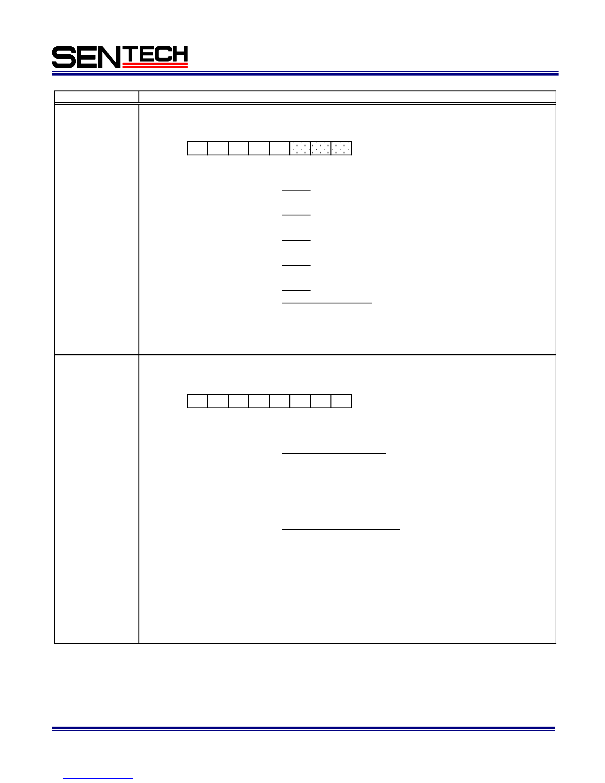
No.11S098-03
57
STC-GE33OX/GEC33OX
Users guide Rev. 1.03
Command No.
F1H:
TEST2[7..0]
D7:
0: Low, 1: High
D6:
0: Low, 1: High
D5:
0: Low, 1: High
D4:
0: Low, 1: High
D3:
0: Low, 1: High
D2 to D0:
No function Sets always as "000"
F8H:
OUTSEL1[7..0]
D7 to D4:
0: FrameTriggerWait signal, 1: UserOutput signal,
2: ExposureActive signal, 3: TriggerAuxiliary signal,
5: SensorReadOut signal,
6 to F: No function
D3 to D0:
0: FrameTriggerWait signal, 1: UserOutput signal,
2: ExposureActive signal, 3: TriggerAuxiliary signal,
5: SensorReadOut signal,
6 to F: No function
Output signal for 5 pin of the power/IO connector
"UserOutput signal for the power/IO connector(TEST2-D3,4)".
Note: When select "UserOutput signal", sets the status of the signal with
4: TriggerInternal signal (after mask and delay process),
(Prohibited setting. Do not set this value)
Note: UserOutput signal is enable when "UserOutput signal" select at enable when "UserOutput sig
Sets the status of the UserOutput signal.
D[7..0]
UserOutput signal for 7pin of the power/IO
UserOutput signal for 6pin of the power/IO
UserOutput signal for 5pin of the power/IO
UserOutput signal for 4pin of the power/IO
UserOutput signal for 3pin of the power/IO
"Output signal selection (OUTSEL)".
[UserOutput signal for the power/IO connector] Initial data: TEST2[7..0] = 00H
[The output signal selection for the power/IO connector] Initial data: OUTSEL1[7..0] = 00H
Sets the output signal from the power/IO connector.
Command descriptions
(Prohibited setting. Do not set this value)
D[7..0]
Output signal for 6 pin of the power/IO connector
4: TriggerInternal signal (after mask and delay process),
D7 D6 D5 D4 D3 D2 D1 D0
D7 D6 D5 D4 D3 D2 D1 D0
Page 58
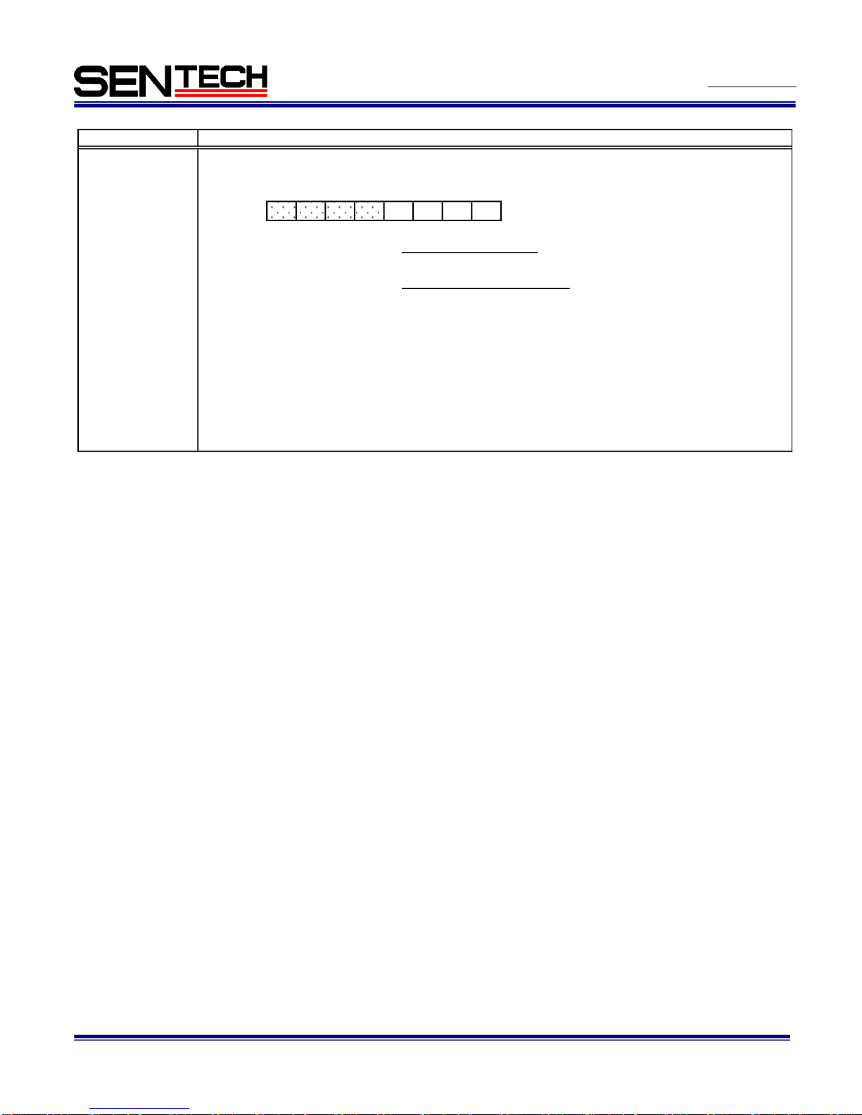
No.11S098-03
58
STC-GE33OX/GEC33OX
Users guide Rev. 1.03
Command No.
F9H:
OUTSEL2[7..0]
D7 to D4: No function Sets always as "0000"
D3 to D0:
0: FrameTriggerWait signal, 1: UserOutput signal,
2: ExposureActive signal, 3: TriggerAuxiliary signal,
5: SensorReadOut signal,
6 to F: No function
Command descriptions
Output signal for 7 pin of the power/IO connector
[The output signal selection for the power/IO connector] Initial data: OUTSEL2[7..0] = 00H
Sets the output signal from the power/IO connector.
D[7..0]
4: TriggerInternal signal (after mask and delay process),
(Prohibited setting. Do not set this value)
Note: When select "UserOutput signal", sets the status of the signal with
"UserOutput signal for the power/IO connector(TEST2-D3,4)".
D7 D6 D5 D4 D3 D2 D1 D0
Page 59
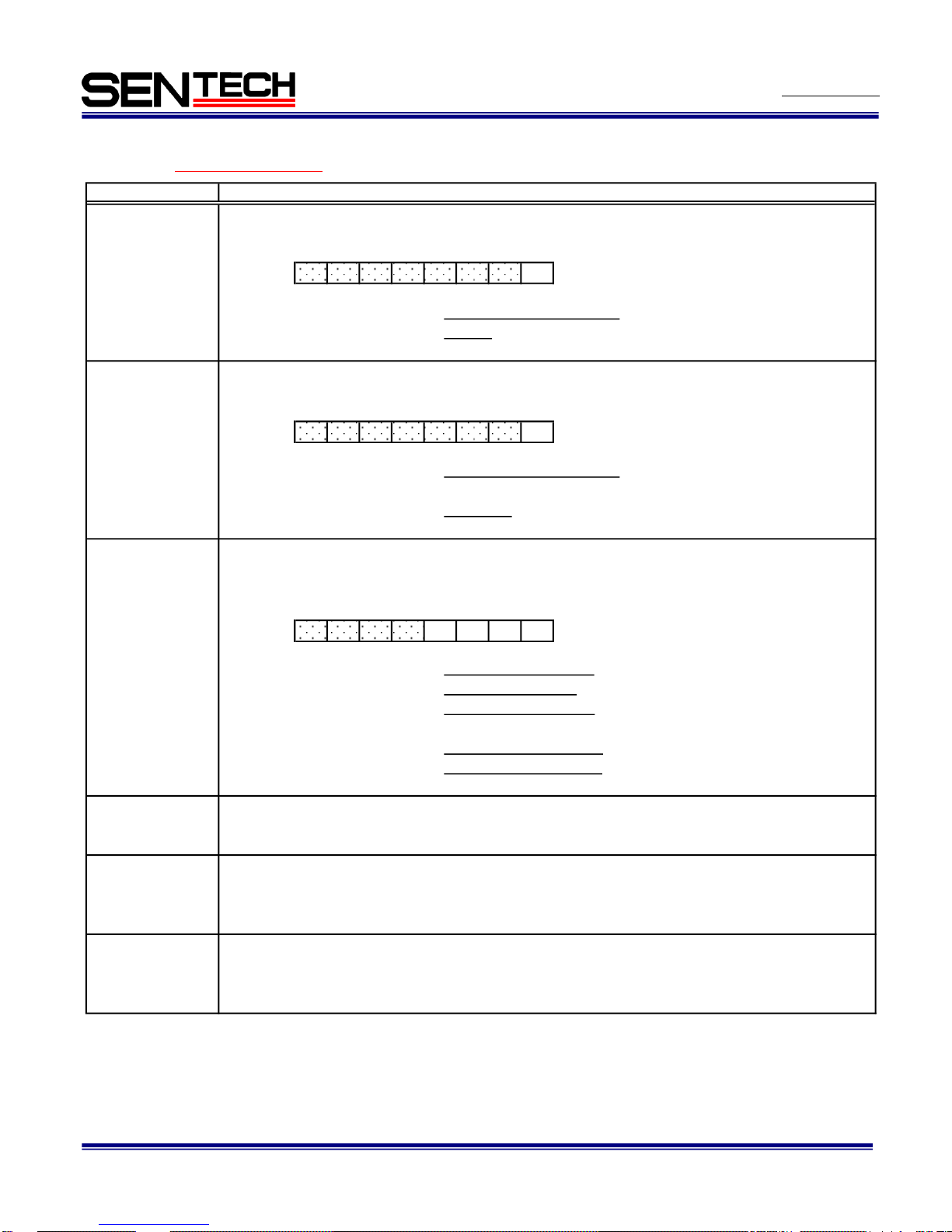
No.11S098-03
59
STC-GE33OX/GEC33OX
Users guide Rev. 1.03
6.4.3 Description of the camera control commands (Device code: 100000)
(The under line settings are the factory default settings)
Command No.
18H:[7..0]
D7 to D1:
No function Sets always as "0000000"
D0: JTAG
0: OFF, 1: ON
19H:[7..0]
D7 to D1:
No function Sets always as "0000000"
D0:
0: Disable, 1: Enable
20H:[7..0]
D7 to D4: No function Sets always as "0000"
D3: AGC
0: OFF (Fixed gain), 1: ON (AGC)
D2: Shutter mode
0: OFF (Fixed shutter), 1: ON (Auto shutter)
D1: Iris lens control method
0: OFF (Manual contro), 1: ON (Auto control)
D0: ALC priority
0: Lens control function, 1: Auto shutter
21H:[7..0]
23H:[7..0]
24H:[15..8]
25H:[20..16]
26H:[7..0]
27H:[15..8]
28H:[20..16]
Sets the lower limit of the electronic shutter for auto shutte as usecond.
[JTAG for the user configurable FPGA] Initial data: 00H
Sets the JTAG connection ON/OFF for the user configurable FPGA.
D[7..0]
[The user configurable FPGA enable] Initial data: 00H
Sets the user configurable FPGA is Enable/Disable when statrt up the camera.
D[7..0]
User configurable FPGA
D[7..0]
[The lower limit of the electronic shutter for auto shutter]
Initial data: 0, data range: 0 to 1,048,575
Sets the maximum limit for the AGC.
Initial data: 11,122, data range: 0 to 1,048,575
Sets the upper limit of the electronic shutter for auto shutte as usecond.
Command descriptions
[The upper limit of the electronic shutter for auto shutter]
[AGC maximum limit] Initial data: 255, data range: 0 to 255
[Exposure mode] Initial data: 00H
Sets the exposure mode, which is the AGC, the shutter mode and
the iris lens control method.
D7 D6 D5 D4 D3 D2 D1 D0
D7 D6 D5 D4 D3 D2 D1 D0
D7 D6 D5 D4 D3 D2 D1 D0
Page 60
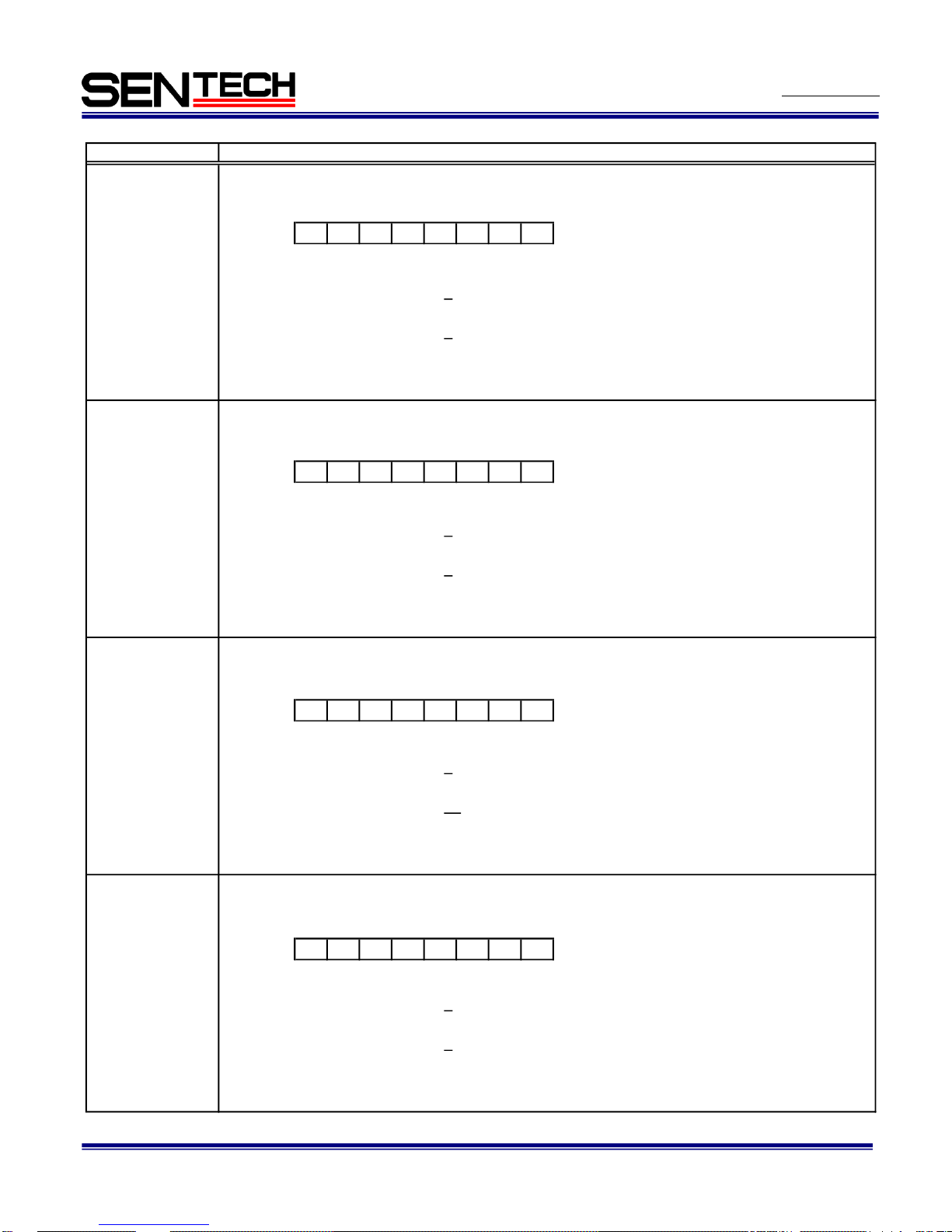
No.11S098-03
60
STC-GE33OX/GEC33OX
Users guide Rev. 1.03
Command No.
29H:[7..0]
D7 to D4: Weight for ALC weight area 2
1, Range: 0 to 15
D3 to D0: Weight for ALC weight area 1
1, Range: 0 to 15
2AH:[7..0]
D7 to D4: Weight for ALC weight area 4
1, Range: 0 to 15
D3 to D0: Weight for ALC weight area 3
1, Range: 0 to 15
2BH:[7..0]
D7 to D4: Weight for ALC weight area 6
1, Range: 0 to 15
D3 to D0: Weight for ALC weight area 5
10, Range: 0 to 15
2CH:[7..0]
D7 to D4: Weight for ALC weight area 8
1, Range: 0 to 15
D3 to D0: Weight for ALC weight area 7
1, Range: 0 to 15
D[7..0]
* Please set the ALC weight area with "30H to 3FH".
D[7..0]
* Please set the ALC weight area with "30H to 3FH".
[Weight4 for ALC] Initial data: 11H
Sets the weight for ALC weight area 7 and 8.
Command descriptions
[Weight3 for ALC] Initial data: 1AH
Sets the weight for ALC weight area 5 and 6.
Sets the weight for ALC weight area 3 and 4.
D[7..0]
[Weight2 for ALC] Initial data: 11H
* Please set the ALC weight area with "30H to 3FH".
* Please set the ALC weight area with "30H to 3FH".
[Weight1 for ALC] Initial data: 11H
Sets the weight for ALC weight area 1 and 2.
D[7..0]
D7 D6 D5 D4 D3 D2 D1 D0
D7 D6 D5 D4 D3 D2 D1 D0
D7 D6 D5 D4 D3 D2 D1 D0
D7 D6 D5 D4 D3 D2 D1 D0
Page 61
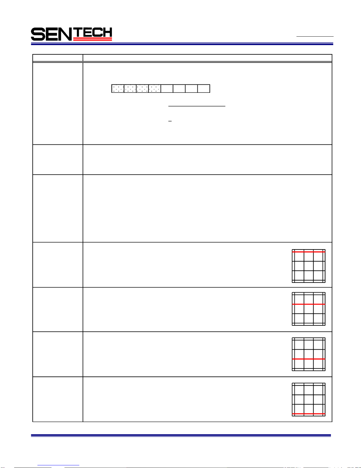
No.11S098-03
61
STC-GE33OX/GEC33OX
Users guide Rev. 1.03
Command No.
2DH:[7..0]
D7 to D4: No function Sets always as "0000"
D3 to D0: Weight for ALC weight area 9
1, Range: 0 to 15
2EH:[7..0]
2FH:[7..0]
the ALC function with the peak brightness of the photometry area.
30H:[7..0]
31H:[15..8]
32H:[7..0]
33H:[15..8]
34H:[7..0]
35H:[15..8]
36H:[7..0]
37H:[15..8]
[Vertical_4 position for the ALC weight area]
Initial data: 462, data range: 0 to 493
Sets the vertical 4 position for ALC weight area.
[Vertical_3 position for the ALC weight area]
Initial data: 298, data range: 0 to 493
Sets the vertical 3 position for ALC weight area.
Sets the vertical 2 position for ALC weight area.
[Vertical_2 position for the ALC weight area]
Command descriptions
[Target brightness for ALC] Initial data: 128, data range: 0 to 255
Sets the target brightness for the ALC function
(AGC, auto shutter or iris lens auto control).
[Weight5 for ALC] Initial data: 01H
Sets the weight for ALC weight area 9.
D[7..0]
* Please set the ALC weight area with "30H to 3FH".
Initial data: 32, data range: 0 to 493
Initial data: 169, data range: 0 to 493
[ALC peak-average] Initial data: 0, data range: 0 to 255
[Vertical_1 position for the ALC weight area]
Sets the control standard for the ACL function (AGC, auto shutter or iris lens auto control).
When set as 0, which is Average: 100%, Peak: 0%,
the ALC function with the average brightness of the photometry area.
When set as 255, which is Average: 0%, Peak: 100%,
Sets the vertical 1 position for ALC weight area.
D7 D6 D5 D4 D3 D2 D1 D0
3
6
9
2
5
8
1
4
7
3
6
9
2
5
8
1
4
7
3
6
9
2
5
8
1
4
7
3
6
9
2
5
8
1
4
7
Page 62
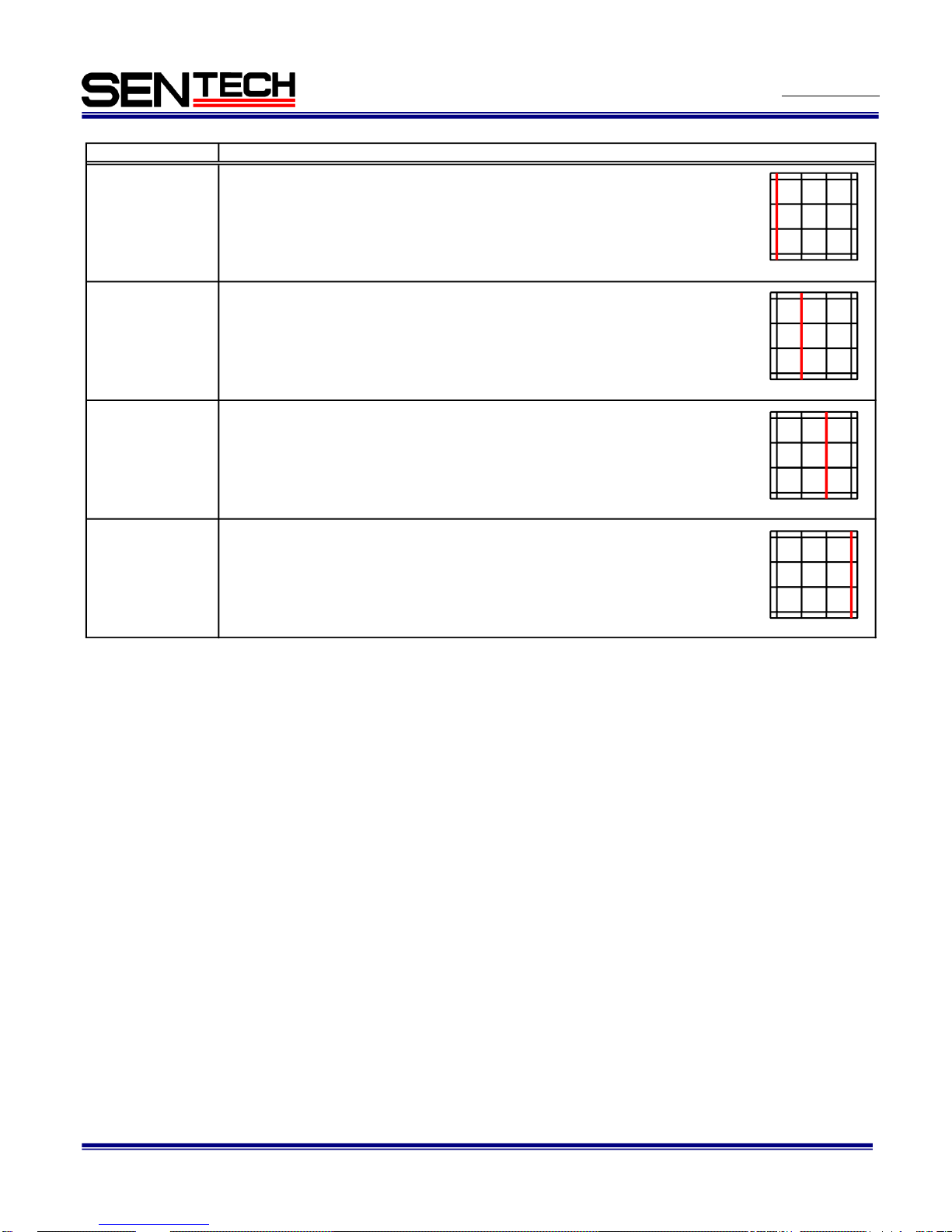
No.11S098-03
62
STC-GE33OX/GEC33OX
Users guide Rev. 1.03
Command No.
38H:[7..0]
39H:[15..8]
3AH:[7..0]
3BH:[15..8]
3CH:[7..0]
3DH:[15..8]
3EH:[7..0]
3FH:[15..8]
Sets the horizontal 1 position for ALC weight area.
Command descriptions
[Horizontal_1 position for the ALC weight area]
Initial data: 36, data range: 0 to 647
[Horizontal_2 position for the ALC weight area]
Initial data: 252, data range: 0 to 647
Sets the horizontal 2 position for ALC weight area.
[Horizontal_3 position for the ALC weight area]
Sets the horizontal 4 position for ALC weight area.
Initial data: 396, data range: 0 to 647
Sets the horizontal 3 position for ALC weight area.
[Horizontal_4 position for the ALC weight area]
Initial data: 612, data range: 0 to 647
3
6
9
2
5
8
1
4
7
3
6
9
2
5
8
1
4
7
3
6
9
2
5
8
1
4
7
3
6
9
2
5
8
1
4
7
Page 63
No.11S098-03
63
STC-GE33OX/GEC33OX
Users guide Rev. 1.03
Command No.
40H:[7..0]
D7 to D4: No function Sets always as "0000"
D3: Push to set white balance operation
0: OFF, 1: ON
D2 to D0: White balance mode
000: OFF, 001: Preset 1,
010: Preset 2, 011: Preset 3,
100: Auto white balance, 101: Push to set white balance,
110 to 111: No function
(Prohibited setting. Do not set these value)
41H:GainR1
[7..0]
* CCD_R: Red of the CCD output image data
42H:GainGr1
[7..0]
* CCD_Gr: Gr of the CCD output image data
43H:GainB1
[7..0]
* CCD_B: Blue of the CCD output image data
Command descriptions
[White balance mode] Initial data: 00H
[Preset_1 white balance (Red gain)] Initial data: 0, data range: 0 to 255
[Preset_1 white balance (Gr gain)] Initial data: 0, data range: 0 to 255
Sets the Red gain for the preset_1 white balance.
Sets the white balance mode for the color camera.
D[7..0]
* When use the push to set white balance, set the white balance mode as
"Push to set white balance" then change "0" to "1" for Push to set white balance operation.
Sets the Gr gain for the preset_1 white balance.
Sets the Blue gain for the preset_1 white balance.
[Preset_1 white balance (Blue gain)] Initial data: 0, data range: 0 to 255
Gr of the camera output image data =
(CCD_Gr - CLAMP Level) x (1 + GainGr1[7..0] / 64) + CLAMP Level
* CLAMP Level:
Clamp level (The calculated value of 38H)
Blue of the camera output image data =
(CCD_R - CLAMP Level) x (1 + GainR1[7..0] / 64) + CLAMP Level
* CLAMP Level:
Clamp level (The calculated value of 38H)
Red of the camera output image data =
(CCD_B - CLAMP Level) x (1 + GainB1[7..0] / 64) + CLAMP Level
* CLAMP Level:
Clamp level (The calculated value of 38H)
D7 D6 D5 D4 D3 D2 D1 D0
Page 64
No.11S098-03
64
STC-GE33OX/GEC33OX
Users guide Rev. 1.03
Command No.
44H:GainGb1
[7..0]
* CCD_Gb: Gb of the CCD output image data
45H:GainR2
[7..0]
* CCD_R: Red of the CCD output image data
46H:GainGr2
[7..0]
* CCD_Gr: Gr of the CCD output image data
47H:GainB2
[7..0]
* CCD_B: Blue of the CCD output image data
48H:GainGb2
[7..0]
* CCD_Gb: Gb of the CCD output image data
Gb of the camera output image data =
(CCD_Gb - CLAMP Level) x (1 + GainGb1[7..0] / 64) + CLAMP Level
* CLAMP Level:
Clamp level (The calculated value of 38H)
Gr of the camera output image data =
(CCD_Gr - CLAMP Level) x (1 + GainGr2[7..0] / 64) + CLAMP Level
* CLAMP Level:
Clamp level (The calculated value of 38H)
* CLAMP Level:
Clamp level (The calculated value of 38H)
Red of the camera output image data =
Sets the Red gain for the preset_2 white balance.
Sets the Gb gain for the preset_1 white balance.
[Preset_1 white balance (Gb gain)] Initial data: 0, data range: 0 to 255
Gb of the camera output image data =
(CCD_Gb - CLAMP Level) x (1 + GainGb1[7..0] / 64) + CLAMP Level
[Preset_2 white balance (Gr gain)] Initial data: 0, data range: 0 to 255
[Preset_2 white balance (Red gain)] Initial data: 0, data range: 0 to 255
(CCD_R - CLAMP Level) x (1 + GainR2[7..0] / 64) + CLAMP Level
* CLAMP Level:
Clamp level (The calculated value of 38H)
Command descriptions
Sets the Blue gain for the preset_2 white balance.
Sets the Gb gain for the preset_2 white balance.
[Preset_2 white balance (Gb gain)] Initial data: 0, data range: 0 to 255
[Preset_2 white balance (Blue gain)] Initial data: 0, data range: 0 to 255
Blue of the camera output image data =
(CCD_B - CLAMP Level) x (1 + GainB2[7..0] / 64) + CLAMP Level
* CLAMP Level:
Clamp level (The calculated value of 38H)
Sets the Gr gain for the preset_2 white balance.
Page 65
No.11S098-03
65
STC-GE33OX/GEC33OX
Users guide Rev. 1.03
Command No.
49H:GainR3
[7..0]
* CCD_R: Red of the CCD output image data
4AH:GainGr3
[7..0]
* CCD_Gr: Gr of the CCD output image data
4BH:GainB3
[7..0]
* CCD_B: Blue of the CCD output image data
4CH:GainGb3
[7..0]
* CCD_Gb: Gb of the CCD output image data
4EH:[7..0]
4FH:[15..8]
[Preset_3 white balance (Gr gain)] Initial data: 0, data range: 0 to 255
Sets the Gr gain for the preset_3 white balance.
Red of the camera output image data =
(CCD_R - CLAMP Level) x (1 + GainR3[7..0] / 64) + CLAMP Level
* CLAMP Level:
Clamp level (The calculated value of 38H)
Sets the bright level threshold for auto white balance process.
Auto white balance process use the color information of the pixel, which is the brightness
of the pixel is greater than this value.
Command descriptions
[Preset_3 white balance (Blue gain)] Initial data: 0, data range: 0 to 255
[Preset_3 white balance (Gb gain)] Initial data: 0, data range: 0 to 255
[Bright level threshold for auto white balance process] Initial data: 3,072, data range: 0 to 4,095
Sets the Gb gain for the preset_3 white balance.
Sets the Blue gain for the preset_3 white balance.
[Preset_3 white balance (Red gain)] Initial data: 0, data range: 0 to 255
Sets the Red gain for the preset_3 white balance.
Gr of the camera output image data =
(CCD_Gr - CLAMP Level) x (1 + GainGr3[7..0] / 64) + CLAMP Level
* CLAMP Level:
Clamp level (The calculated value of 38H)
Gb of the camera output image data =
(CCD_Gb - CLAMP Level) x (1 + GainGb3[7..0] / 64) + CLAMP Level
* CLAMP Level:
Clamp level (The calculated value of 38H)
Blue of the camera output image data =
(CCD_B - CLAMP Level) x (1 + GainB3[7..0] / 64) + CLAMP Level
* CLAMP Level:
Clamp level (The calculated value of 38H)
Page 66
No.11S098-03
66
STC-GE33OX/GEC33OX
Users guide Rev. 1.03
Command No.
50H:[7..0]
51H:[15..8]
52H:[7..0]
53H:[15..8]
54H:[7..0]
55H:[15..8]
56H:[7..0]
57H:[15..8]
58H:[7..0]
59H:[15..8]
white balance area.
5AH:[7..0]
5BH:[15..8]
white balance area.
push to set white balance.
5CH:[7..0]
5DH:[15..8]
white balance area.
5EH:[7..0]
5FH:[15..8]
Sets the horizontal 2 position, which is the horizontal end position for
white balance area.
This aread use for the gain calcuration for auto white balance and
push to set white balance.
Command descriptions
[X_offset for AOI]
[Horizontal_2 position for the white balance area]
Initial data: 647, data range: 0 to 647
Sets the X_offset, which is the horizontal start position of the image for the AOI.
[Y_offset for AOI]
Sets the Y_offset, which is the vertical start position of the image for the AOI.
Initial data: 494, data range: 2 <= "Y_offset + Height" <= 494
[Height for AOI]
Sets the height, which is the vertical size of the image for the AOI.
Initial data: 0, data range: 2 <= "Y_offset + Height" <= 494
Initial data: 0, data range: 8 <= "X_offset + Width" <= 648
[Width for AOI]
Initial data: 648, data range: 8 <= "X_offset + Width" <= 648
Sets the width, which is the horizontal size of the image for the AOI.
[Vertical_1 position for the white balance area]
Initial data: 0, data range: 0 to 493
Sets the vertical 1 position, which is the vertical start position for
This aread use for the gain calcuration for auto white balance and
push to set white balance.
[Vertical_2 position for the white balance area]
Initial data: 493, data range: 0 to 493
Sets the vertical 2 position, which is the vertical end position fo
This aread use for the gain calcuration for auto white balance and
push to set white balance.
[Horizontal_1 position for the white balance area]
Initial data: 0, data range: 0 to 647
Sets the horizontal 1 position, which is the horizontal start position for
This aread use for the gain calcuration for auto white balance and
Page 67
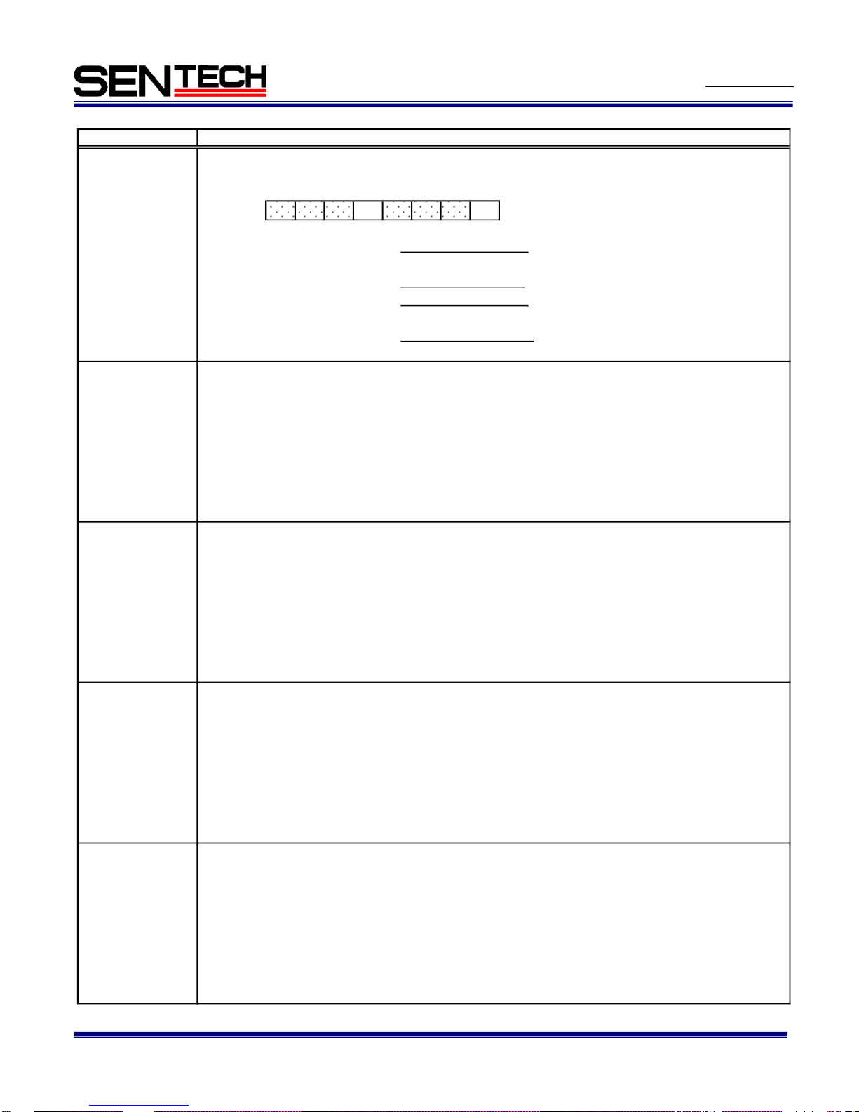
No.11S098-03
67
STC-GE33OX/GEC33OX
Users guide Rev. 1.03
Command No.
60H:[7..0]
D7 to D5: No function Sets always as "000"
D4:
0: OFF (Full screen), 1: ON (setup area)
D3 to D1: No function Sets always as "000"
D0:
0: OFF (Gamma=1.0), 1: ON
80H:
GainRP
[7..0]
* CCD_R: Red of the CCD output image data
81H:
GainGrP
[7..0]
* CCD_Gr: Gr of the CCD output image data
82H:
GainBR
[7..0]
* CCD_B: Blue of the CCD output image data
83H:
GainGbP
[7..0]
* CCD_Gb: Gb of the CCD output image data
Command descriptions
[Camera mode1] Initial data: 00H
[Push to set white balance (Red gain)] Initial data: 0, data range: 0 to 255
Sets the Red gain for the Push to set white balance.
Gamma table ON/OFF
White balance area ON/OFF
D[7..0]
Sets the white balance area ON/OFF and the gamma table ON/OFF.
Red of the camera output image data =
(CCD_R - CLAMP Level) x (1 + GainRP[7..0] / 64) + CLAMP Level
* CLAMP Level:
Clamp level (The calculated value of 38H)
[Push to set white balance (Gr gain)] Initial data: 0, data range: 0 to 255
Sets the Gr gain for the Push to set white balance.
Gr of the camera output image data =
(CCD_Gr - CLAMP Level) x (1 + GainGrP[7..0] / 64) + CLAMP Level
* CLAMP Level:
Clamp level (The calculated value of 38H)
[Push to set white balance (Blue gain)] Initial data: 0, data range: 0 to 255
Sets the Blue gain for the Push to set white balance.
Blue of the camera output image data =
(CCD_B - CLAMP Level) x (1 + GainBR[7..0] / 64) + CLAMP Level
* CLAMP Level:
Clamp level (The calculated value of 38H)
[Push to set white balance (Gb gain)] Initial data: 0, data range: 0 to 255
Sets the Gb gain for the Push to set white balance.
Gb of the camera output image data =
(CCD_Gb - CLAMP Level) x (1 + GainGbP[7..0] / 64) + CLAMP Level
* CLAMP Level:
Clamp level (The calculated value of 38H)
D7 D6 D5 D4 D3 D2 D1 D0
Page 68
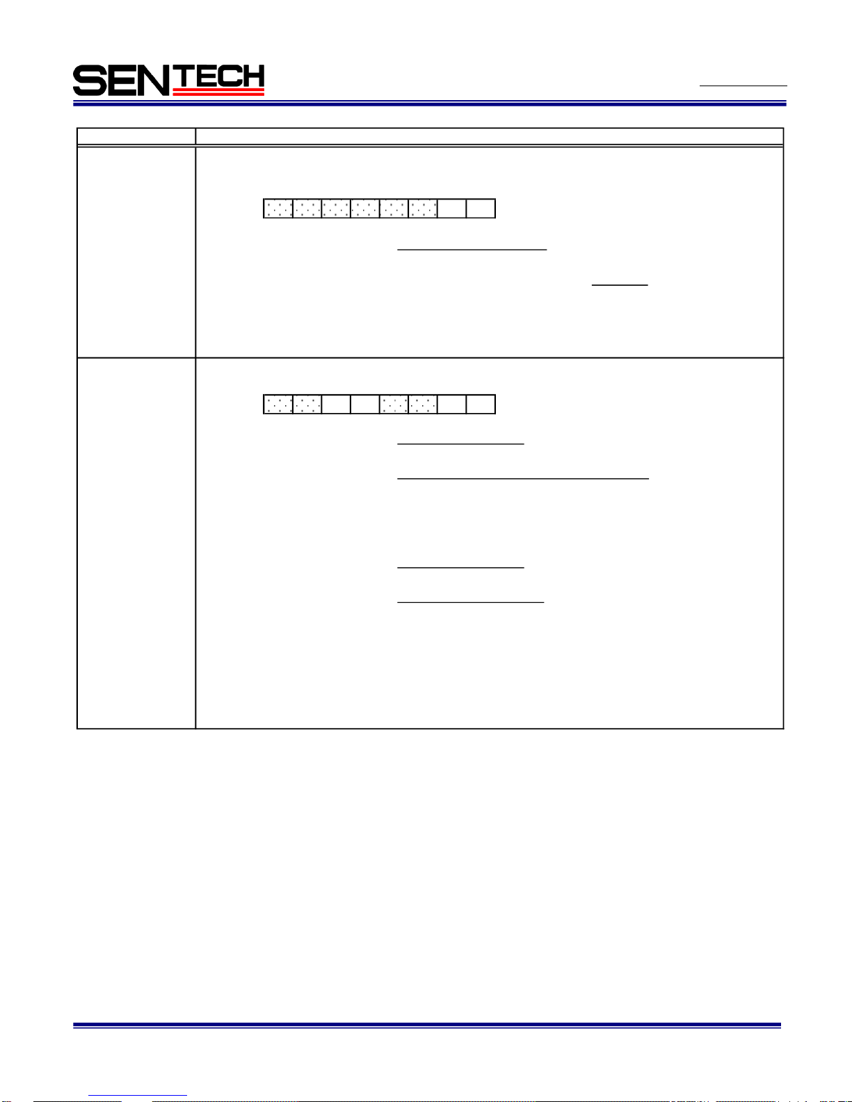
No.11S098-03
68
STC-GE33OX/GEC33OX
Users guide Rev. 1.03
Command No.
92H:[7..0]
D7 to D2: No function Sets always as "000000"
D1 to D0:
00: Hold,
01: Open,
10: Close,
11: No fucntion
(Prohibited setting. Do not set this value)
C0H:[7..0]
D7 to D6: No function Sets alwayas as "00"
D5 to D4:
11: Color interpolation
D3 to D2: No function Sets alwayas as "00"
D1 to D0:
(Prohibited setting. Do not set this value)
Command descriptions
Manual adjustment operation
[Iris lens manual adjustment] Initial data: 01H
Sets the iris lens manual adjustment operation.
D[7..0]
[Image data between FPGAs] Initial data: 00H
D[7..0]
Image process after the image data from the user configurable FPGA
00: No process (No data from use FPGA),
(No image data from the use configurable FPGA)
01: White balance, gamma and color interpolation,
10: Gamma and color interpolation,
11: No function
Note: White balance and color interpolation process are available only for color camera.
Image data from Sentech FPGA to the user configurable FPGA
00: CCD out image data,
01: White balance processed image data,
10: White balance and gamma processed image data,
D7 D6 D5 D4 D3 D2 D1 D0
D7 D6 D5 D4 D3 D2 D1 D0
Page 69
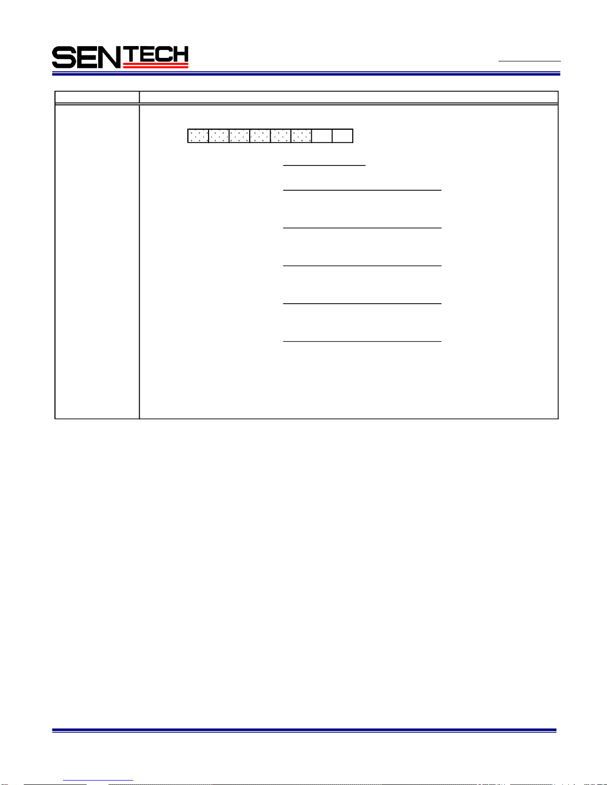
No.11S098-03
69
STC-GE33OX/GEC33OX
Users guide Rev. 1.03
Command No.
C1H:[7..0]
D7 to D5: No function Please sets as 000
D4:
D3:
D2:
D1:
D0:
Note: When select "Output signal from Sentech FPGA",
"Output signal selection (F0H, F8H and F9H)".
select output signal from Sentech FPGA for the power/IO connector with
Output signal for 4 pin (Out1) of the power/IO connector
Output signal for 3 pin (Out0) of the power/IO connector
0: Output signal from Sentech FPGA,
1: Output signal from the user configurable FPGA
Output signal for 6 pin (Out3) of the power/IO connector
1: Output signal from the user configurable FPGA
Output signal for 5 pin (Out2) of the power/IO connector
0: Output signal from Sentech FPGA,
0: Output signal from Sentech FPGA,
1: Output signal from the user configurable FPGA
0: Output signal from Sentech FPGA,
1: Output signal from the user configurable FPGA
Command descriptions
D[7..0]
1: Output signal from the user configurable FPGA
[Output signal selection] Initial data: 00H
Output signal for 7 pin (Out4) of the power/IO connector
0: Output signal from Sentech FPGA,
D7 D6 D5 D4 D3 D2 D1 D0
Page 70

No.11S098-03
70
STC-GE33OX/GEC33OX
Users guide Rev. 1.03
6.4.4 Sequence for the command saves to the EEPROM
Please use below sequence for the command saves to the EEPROM
1) Set “1” to the 80H.0 for the accept “write control to the EEPROM”.
2) Send the command and the save data with the EEPROM access command, which is set “1” for the page
selection.
3) The camera send back the one of the below receiving code after write EEPROM.
01H: OK
17H: EEPROM write error
4) 80H.0 is changed to “0” automatically after write EEPROM.
Note.1) DO NOT saves to the EEPROM when 80H.0 is “0”.
Note.2) When save the multiple sequence command to the EEPROM, all data save to the EEPROM by one
operation from 1) to 4).
Example of the multiple sequence command: “10H, 11H, 12H and 13H” or “22H, 23H and 24H”.
Note.3) When save the multiple command data, which is not sequence command, to the EEPROM, it is
necessary to operate the number of times from 1) to 4).
Example of the multiple command: “10H, 13H, 19H and 1BH” or “20H, 23H and 25H”.
Page 71
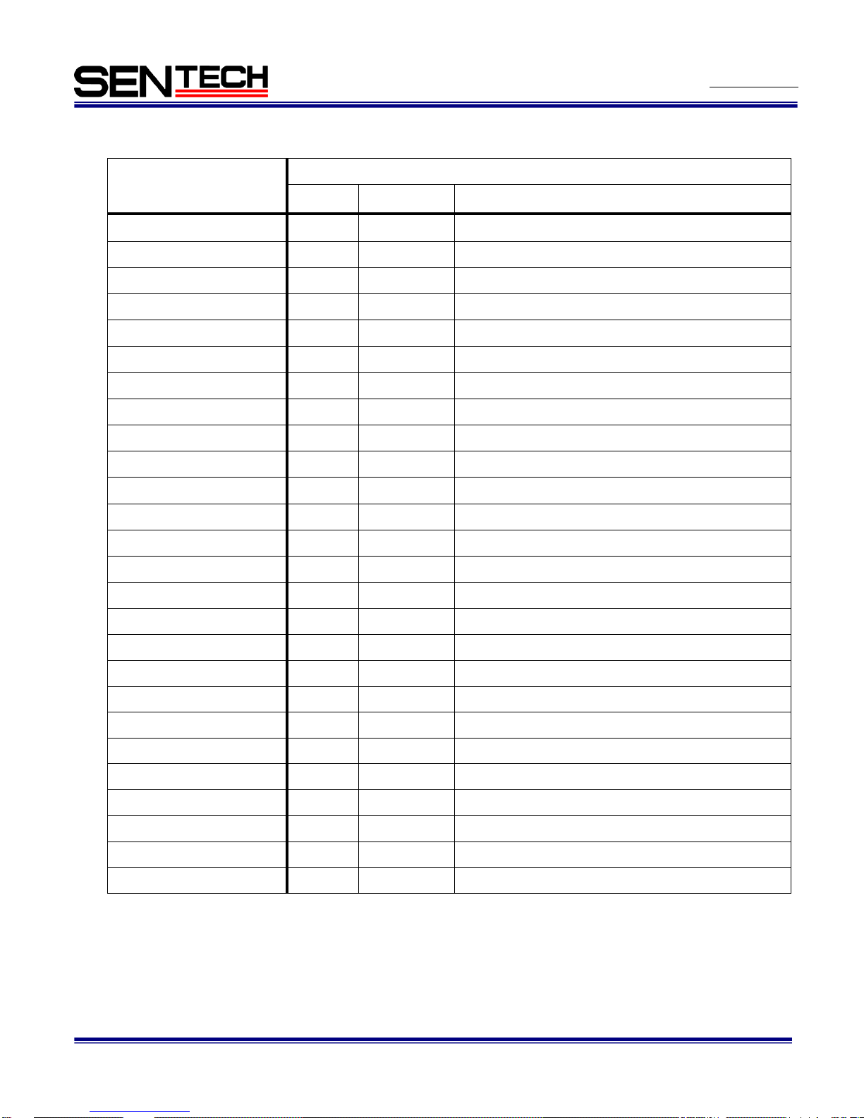
No.11S098-03
71
STC-GE33OX/GEC33OX
Users guide Rev. 1.03
6.5 GenICam command / Camera command reference table
GenICam command
Camera command
Device
Command
Function
Width
100000
56-57H
Width for AOI
Height
100000
52-53H
Height for AOI
PixelFormat
000000
19H.0-2
Video out
OffsetX
100000
54-55H
X offset for AOI
OffsetY
100000
50-51H
Y offset for AOI
BinningVertical
000000
10H.4
Binning
ExposureMode
000000
10H.5
Trigger mode
ExposureTimeRaw
000000
20-22H
Exposure time of the electronic shutter
ExposureAuto
100000
20H.2
Shutter mode
AcquistionFrameRate
000000
58-5CH
Frame rate
TriggerDelay
000000
50-53H
The delay time for the trigger signal
TriggerActivation
000000
10H.6
Trigger polarity
TriggerSource
000000
12H.5
Trigger signal type
TriggerSoftware
000000
16H.0
Generate command software trigger
TriggerSoftwareSource
000000
16H.6-7
Software trigger source selection
TriggerMode
000000
11H.3
Function mode
LineSource0
000000
F0H.0-3
Output signal for 3 pin of the power/IO connector
LineSource1
000000
F0H.4-7
Output signal for 4 pin of the power/IO connector
LineSource2
000000
F8H.0-3
Output signal for 5 pin of the power/IO connector
LineSource3
000000
F8H.4-7
Output signal for 6 pin of the power/IO connector
LineSource4
000000
F9H.0-3
Output signal for 7 pin of the power/IO connector
UserOutputValue0
000000
F1H.3
UserOutput signal for 3 pin of the power/IO connector
UserOutputValue1
000000
F1H.4
UserOutput signal for 4 pin of the power/IO connector
UserOutputValue2
000000
F1H.5
UserOutput signal for 5 pin of the power/IO connector
UserOutputValue3
000000
F1H.6
UserOutput signal for 6 pin of the power/IO connector
UserOutputValue4
000000
F1H.7
UserOutput signal for 7 pin of the power/IO connector
Page 72
No.11S098-03
72
STC-GE33OX/GEC33OX
Users guide Rev. 1.03
GenICam command
Camera command
Device
Command
Function
LineInverter0
000000
5DH.0
Output signal’s polarity for 3 pin of the power/IO
connector
LineInverter1
000000
5DH.1
Output signal’s polarity for 4 pin of the power/IO
connector
LineInverter2
000000
5DH.2
Output signal’s polarity for 5 pin of the power/IO
connector
LineInverter3
000000
5DH.3
Output signal’s polarity for 6 pin of the power/IO
connector
LineInverter4
000000
5DH.4
Output signal’s polarity for 7 pin of the power/IO
connector
StrobeSignalOnTime
000000
90-93H
Strobe signal active time
StrobeSignalDelay
000000
54-57H
The delay time for the strobe signal
Page 73
No.11S098-03
73
STC-GE33OX/GEC33OX
Users guide Rev. 1.03
GenICam command
Camera command
Device
Command
Function
BalanceWhiteAuto
100000
40H.0-2
White balance mode
BalanceRatio_R_Preset1
100000
41H
Preset1 white balance (Red gain)
BalanceRatio_Gr_Preset1
100000
42H
Preset1 white balance (Gr gain)
BalanceRatio_B_Preset1
100000
43H
Preset1 white balance (Blue gain)
BalanceRatio_Gb_Preset1
100000
44H
Preset1 white balance (Gb gain)
BalanceRatio_R_Preset2
100000
45H
Preset2 white balance (Red gain)
BalanceRatio_Gr_Preset2
100000
46H
Preset2 white balance (Gr gain)
BalanceRatio_B_Preset2
100000
47H
Preset2 white balance (Blue gain)
BalanceRatio_Gb_Preset2
100000
48H
Preset2 white balance (Gb gain)
BalanceRatio_R_Preset3
100000
49H
Preset3 white balance (Red gain)
BalanceRatio_Gr_Preset3
100000
4AH
Preset3 white balance (Gr gain)
BalanceRatio_B_Preset3
100000
4BH
Preset3 white balance (Blue gain)
BalanceRatio_Gb_Preset3
100000
4CH
Preset3 white balance (Gb gain)
BalanceRatio_R_Once
100000
80H
Push to set white balance (Red gain)
BalanceRatio_Gr_Once
100000
81H
Push to set white balance (Gr gain)
BalanceRatio_B_Once
100000
82H
Push to set white balance (Blue gain)
BalanceRatio_Gb_Once
100000
83H
Push to set white balance (Gb gain)
GainAuto
100000
20H.3
AGC
GainRaw
000000
30H
CDS gain
BlackLevelRaw
000000
38H
Clamp level
SmearHalfReduction
000000
11H.4
Smear half reduction
GammaMode
100000
60H.0
Gamma table ON/OFF
LensManualAdjustment
100000
92H.0-1
Iris lens manual adjustment operation
PriorityMode
100000
20H.0
ALC control method priority
ALCIrisLens
100000
20H.1
Iris lens control method
Min_ShutterTime
100000
26-28H
The lower limit of the electronic shutter for auto shutter
Max_ShutterTime
100000
23-25H
The upper limit of the electronic shutter for auto shutter
AGCRange
100000
21H
AGC maximum limit
TargetBrightness
100000
2EH
Target brightness for ALC
ALC_Peak_Average
100000
2FH
ALC peak-average
DigitalGain
000000
31H
The digital gain
Page 74
No.11S098-03
74
STC-GE33OX/GEC33OX
Users guide Rev. 1.03
GenICam command
Camera command
Device
Command
Function
ALCWeight1
100000
29H.0-3
Weight1 for ALC
ALCWeight2
100000
29H.4-7
Weight2 for ALC
ALCWeight3
100000
2AH.0-3
Weight3 for ALC
ALCWeight4
100000
2AH.4-7
Weight4 for ALC
ALCWeight5
100000
2BH.0-3
Weight5 for ALC
ALCWeight6
100000
2BH.4-7
Weight6 for ALC
ALCWeight7
100000
2CH.0-3
Weight7 for ALC
ALCWeight8
100000
2CH.4-7
Weight8 for ALC
ALCWeight9
100000
2DH.0-3
Weight9 for ALC
ALCWindowV1
100000
30-31H
Vertical1 position for the ALC weight area
ALCWindowV2
100000
32-33H
Vertical2 position for the ALC weight area
ALCWindowV3
100000
34-35H
Vertical3 position for the ALC weight area
ALCWindowV4
100000
36-37H
Vertical4 position for the ALC weight area
ALCWindowH1
100000
38-39H
Horizontal1 position for the ALC weight area
ALCWindowH2
100000
3A-3BH
Horizontal2 position for the ALC weight area
ALCWindowH3
100000
3C-3DH
Horizontal3 position for the ALC weight area
ALCWindowH4
100000
3E-3FH
Horizontal4 position for the ALC weight area
WB_WindowH1
100000
58-59H
Vertical1 position for the white balance area
WB_WindowH2
100000
5A-5BH
Vertical2 position for the white balance area
WB_WindowV1
100000
5C-5DH
Horizontal1 position for the white balance area
WB_WindowV2
100000
5E-5FH
Horizontal2 position for the white balance area
WB_WindowMode
100000
60H.4
White balance area ON/OFF
YThreshold
100000
4E-4FH
Bright level threshold for auto white balance
ALCWeight4
100000
2AH.4-7
Weight4 for ALC
ALCWeight5
100000
2BH.0-3
Weight5 for ALC
Page 75

No.11S098-03
75
STC-GE33OX/GEC33OX
Users guide Rev. 1.03
Caution:
Width, Height and PixelFormat are effect to the image data size.
Please use GenICam command name command when change these values like below sample code.
In the case to change the Width
BOOL SetWidth( PvDevice *pDevice, PvInt64 lValue )
{
PvGenInteger* lGenInteger = dynamic_cast<PvGenInteger*>( pDevice->GetGenParameters()->Get( "Width" ) );
PvResult lResult = lGenInteger->SetValue(lValue);
return lResult.IsOK();
}
Page 76

No.11S098-03
76
STC-GE33OX/GEC33OX
Users guide Rev. 1.03
9F Ebina Prime Tower. 9-50 Chuo 2 Chome
Ebina-city, Kanagawa
243-0432, JAPAN
Sentech Co., Ltd
TEL +81-46-236-6660 FAX +81-46-236-6661
URL http://www.sentech.co.jp/
 Loading...