

Page 1
1/20
Product Name
MM Chip Reader / Writer module [UHF]
Product Number
MMRW-MD-U01
MMRW User Manual
FEC International (M) SDN BHD
2nd Nov. 2011
Page 2

2/20
Contents
1 Introduction ..........................................................................................................................................................3
2 Usage Important Points .........................................................................................................................................3
3 Key features .........................................................................................................................................................3
4 Reader/writer module package content ....................................................................................................................4
5 Connections..........................................................................................................................................................5
6 Function and use ...................................................................................................................................................5
7 Hardware .............................................................................................................................................................6
7.1 Transmitting circuit .......................................................................................................................................6
7.2 Receiving circuit / comparator circuit .............................................................................................................7
7.3 Microprocessor .............................................................................................................................................8
7.4 Microprocessor’s pin assignment ................................................................................................................. 10
7.5 RF antenna ................................................................................................................................................. 10
8 Firmware............................................................................................................................................................ 11
9 Firmware Writing Procedures............................................................................................................................... 12
9.1 Firmware writing application start-up and installation .................................................................................... 12
9.2 Firmware writing ........................................................................................................................................ 12
10 Product general specification................................................................................................................................ 16
11 Annexes ............................................................................................................................................................. 17
11.1 Schematics ................................................................................................................................ ................. 17
11.2 List of components ..................................................................................................................................... 18
11.3 Antenna layout ........................................................................................................................................... 20
12 FCC STATEMENT ............................................................................................................................................. 20
Page 3

3/20
1 Introduction
This MMRW-MD-U01 is a reader/writer module complied with multiband RFID chip dubbed as “MM Chip”.
This document contains the instructions to use and evaluate the functions and the performance of this device.
For external interface connection, either USB or UART serial connection can be applied, which is applicable to
almost all of the controller systems.
For more details on the product specifications, please refer to “MMRW-U02 Product Specification Document”.
2 Usage Important Points
[Regulation/Standards]
This product follows the guidance for reading/writing communication equipment. It is important to check the
regulation/standard and the seller or user of the intended country.
[Points to take notes before using the product]
1) This product is designed for general use and should not be utilized with application such as medical
appliances related to human life or in space satellite environment which requires high reliability. Our
company will not be responsible for any accidents caused from the said events, such as personal accident,
fire accident or any public related accident.
2) This product is emitting radio wave which can affect medical appliances such as the pacemaker device.
3) Do not place this product near any radio device since it can cause interference.
4) Do not touch the connector terminal as it can result in electrical shock and will eventually destroy the
product.
3 Key features
Support MM2 chip air interface protocol and commands
Light weight, compact size module
UART serial and USB communication available
RF output: 100mW
Operation voltage: 5VDC
Page 4
4/20
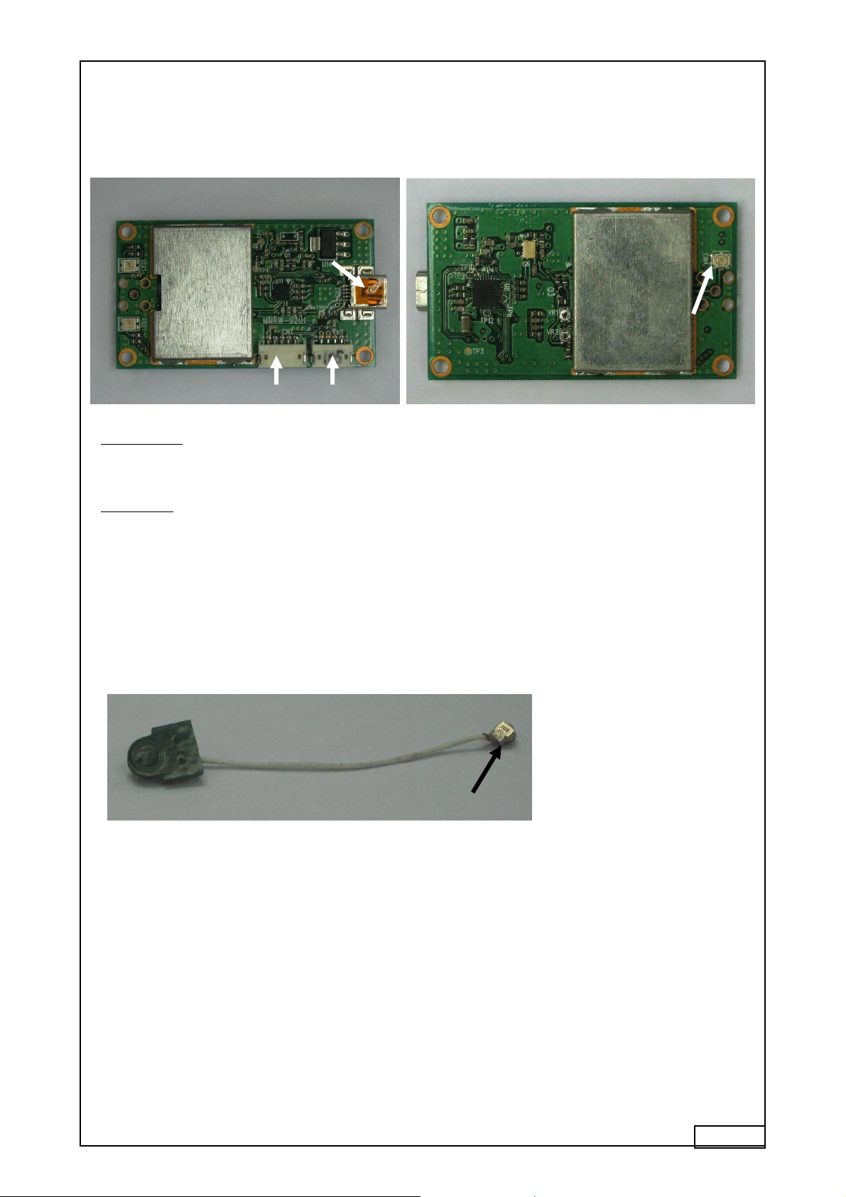
Top side
Back side
Min-USB
UART
Antenna connector
Antenna
connector
5pin for F/W writing
4 Reader/writer module package content
[RFID reader / writer board: MMRW-MD-U01]
USB (Mini B)
Packet communication complies with USB2.0/1.1
UART serial
Communication speed
Variable according to a command (default:9,600bps)
(1,200/2,400/4,800/9,600/19,200/38,400/57,600bps)
Data bit: 8bit
Stop bit: 1bit
Parity bit: N/A
Flow control: N/A
[Board antenna: MMATU-OCA]
[CD with SDK and documentation]
Included in the CD are SDK and related documents, product specifications and various manuals. For more details,
please see “readme.txt” included in the CD.
Page 5
5/20
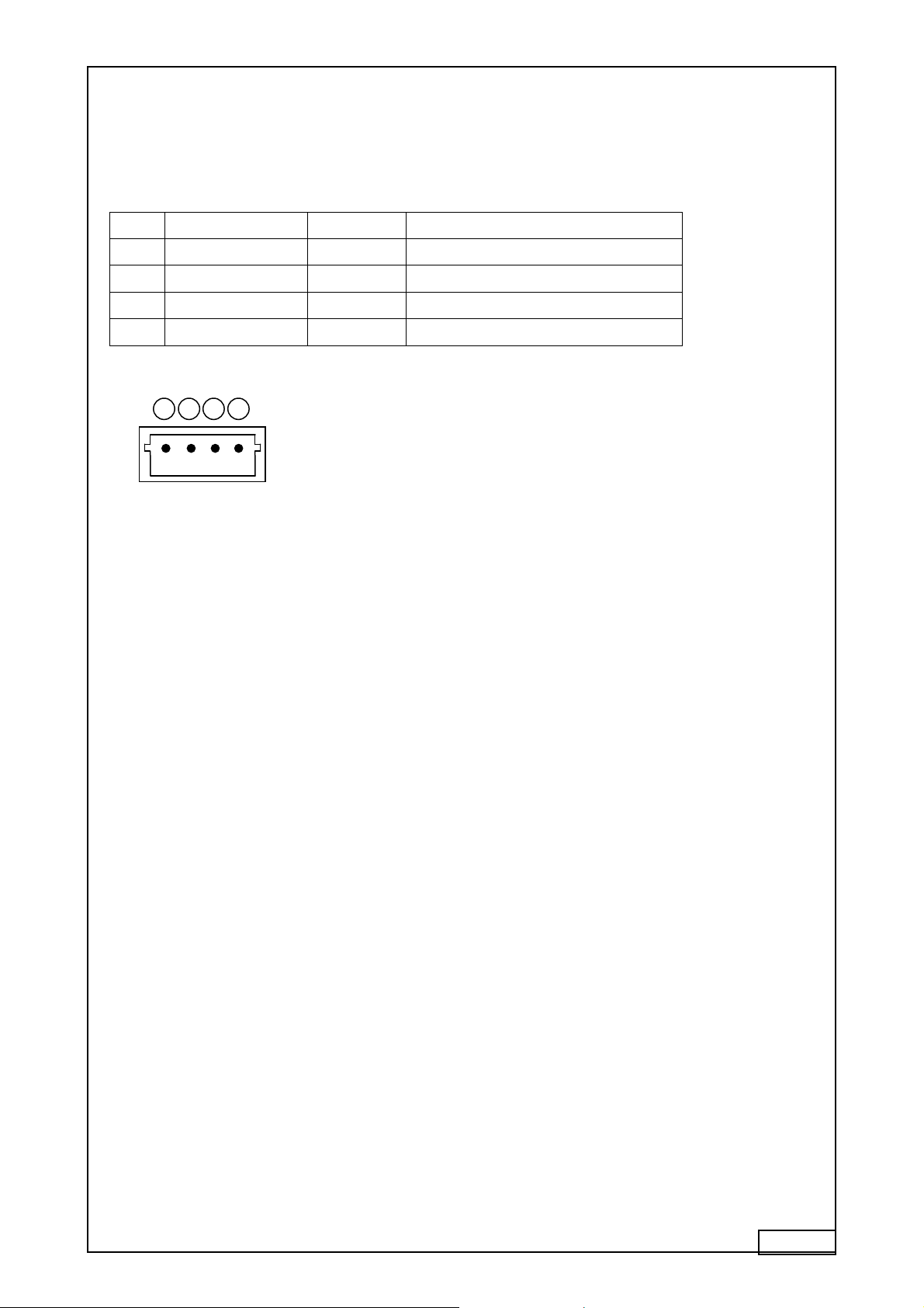
No.
Signal name
I/O
Content
1
VCC
-
Provide DC 5V (+/-0.25V)
2
GND
-
GND
3
TXD
OUT
UART serial signal output (LV-TTL)
4
RXD
IN
UART serial signal input (LV-TTL)
5 Connections
The first step is to connect the components. Connect antenna board to the RFID reader / writer board using the
connector. Terminal and reader/writer can be connected by USB or UART serial port.
Pin assignment for UART serial is stated in the table below. Please prepare a harness cable for the connection to
device terminal.
[Pin assignment]
6 Function and use
The equipment is ready to be operated once all connections are completed.
Next, equipment operating with SDK package will be explained. SDK Package is prepared for application
development of MMRW series. SDK Package contains demo software, USB driver, USB communication library,
and sample source code. For further details, please refer to “Demo Software Manual” before using MMRW
demo software.
Please refer to “MMRW Command Library Function Specification” to develop application.
Page 6
6/20
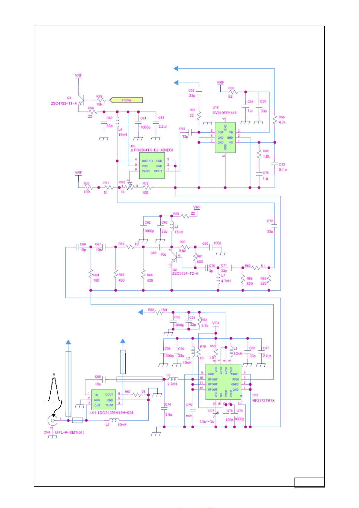
Fig 1
Rx carrier out
LBT carrier out
Tx data in
U11-14pin VCO oscillator feedback
XTX SW
U5-12pin VCO Control voltage
⑤
7 Hardware
7.1 Transmitting circuit
Fig1 is Transmitting circuit. When VCO Control voltage from U11 PLL Synthesizer LMX2433 12pin is input,
VCO SV910ER1418 of U18 oscillate the 919.0MHz - 923.0MHz (Malaysia band, waveform ①). C53 output
is an oscillator feedback out for U15. Oscillating out can control Gain with Gain Control Amplifier of U20 μ
Page 7
7/20
Fig 2
⑥
U10-5pin
Comparator level
⑩
⑦
⑧
⑨
⑪
PC8204 and VR2. It does input to Q2 high frequency amplifier transistor base and outputs waveform ③. R63,
R68 and R69 are -1dB πtype attenuator. U19 RF2173 is a high frequency power amplifier. It becomes ASK
modulation (waveform ④) by Tx data Signal from U5 TC7S14. And, it is adjusted to 10% modulation with
R50. U19’s out outputs Tx carrier (waveform ⑤) from ANT out by passing U17 Directional coupler. Tx
carrier level is adjusted to 100mW with VR1.
7.2 Receiving circuit / comparator circuit
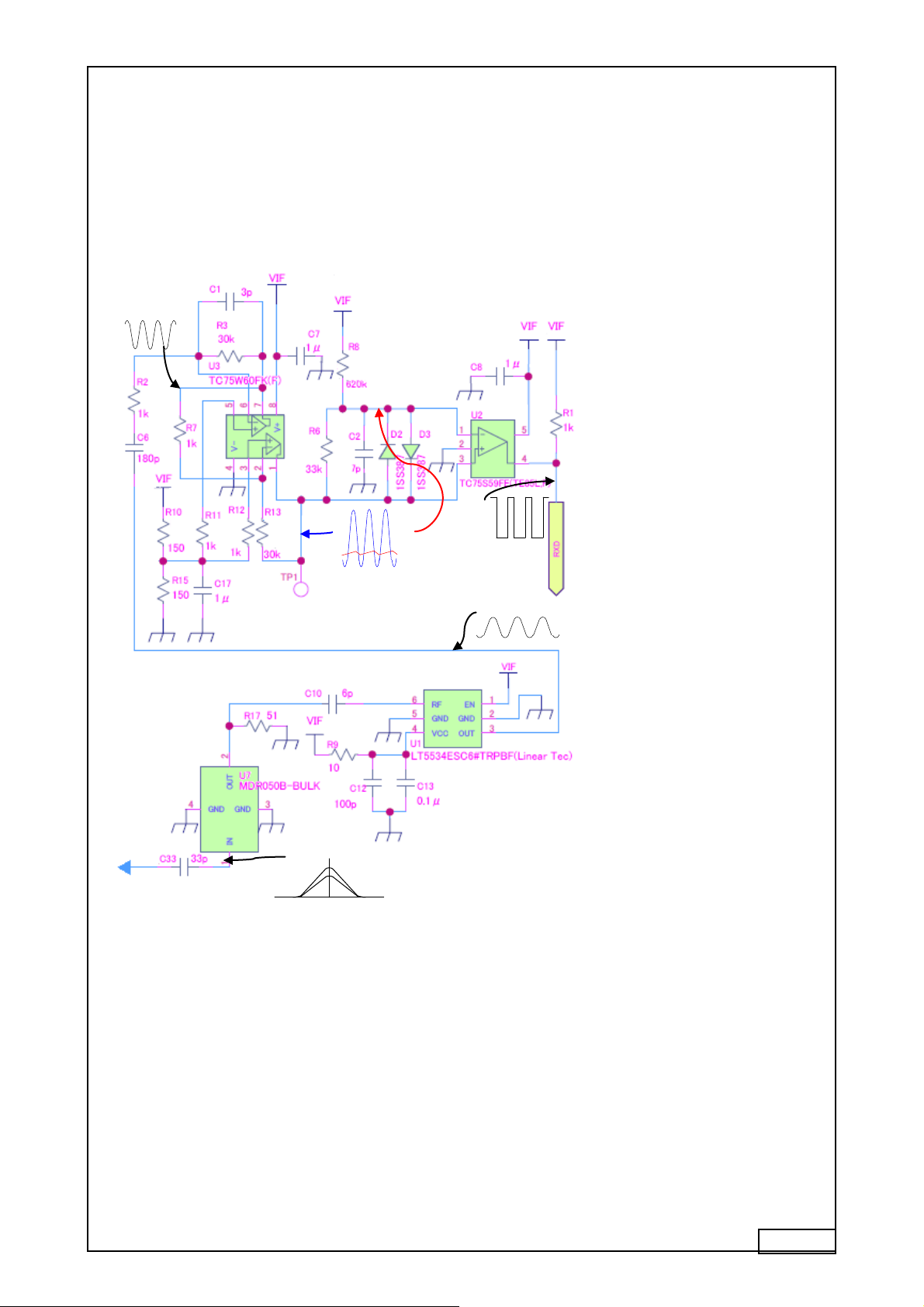
Fig 2 shows receiving circuit / comparator circuit. Career Signal (waveform ⑥) input from U10-5pin passes
U7 band pass filter, and outputs career wave (waveform ⑦) at U1 high frequency amplifier/detect IC LT5534.
Career wave is amplified by U3 operational amplifier TC75W60 and outputs waveform⑧, ⑨. Waveform ⑨
inputs to U2 Comparator TC75S59 non inverting input. Other waveform ⑨ becomes threshold Signal ⑩ by
R6 and C3 integrating circuit. It inputs to inverting input and outputs Rx data out (waveform ⑪) to U8-1pin
and 2pin.
Page 8
8/20
Fig 3
Tx data out
U9-2pin RF Switch out
R58 VCO Control
C53 VCO Career Feedback in
U2-4pin Rx data in
7.3 Microprocessor
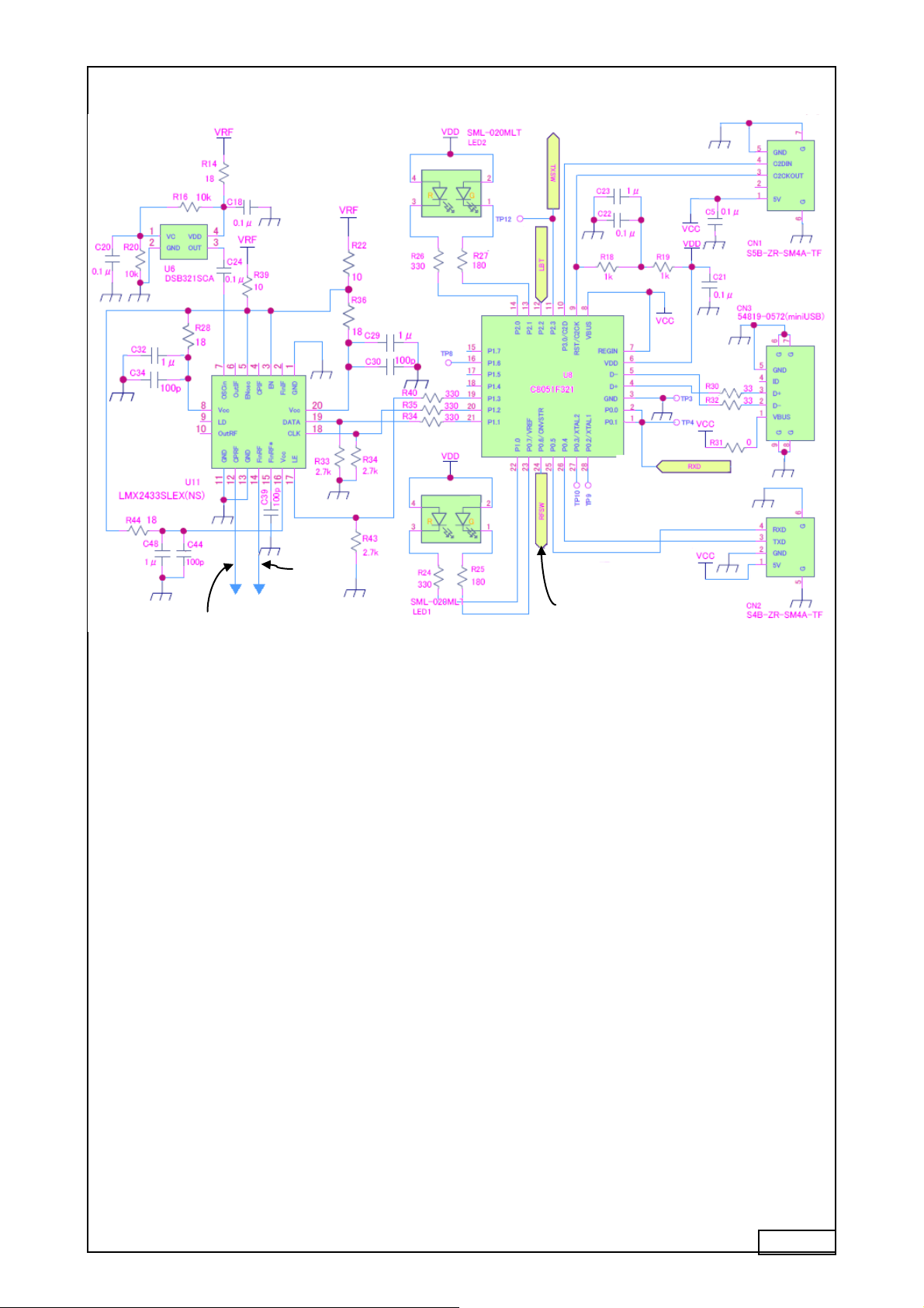
Fig3 shows circuit that centers on U8 C8051F321 microprocessor. It is composed of LED drive, USB interface,
serial data interface, U6 career oscillator, U11 PLL Synthesizer, and power reset circuit. The crystal oscillator is
unnecessary, because clock generator is built-in. Moreover, 3.3V voltage regulator and USB driver are built into
it. 3.3V constant voltage is output from 6Pin. This Vdd is used so as not to change brightness of LED by the Vcc
change. R18, R19, C22, and C23 are for set time constant. CN3 is USB interface connector, and CN4 is a
connector for the serial interface. CN1 is CPU firmware write connector. CN4-1Pin must use 5V when you
use the serial interface connector.
Page 9
9/20
Fig 4
3.8V
3.5V
3V
3.3V
5V
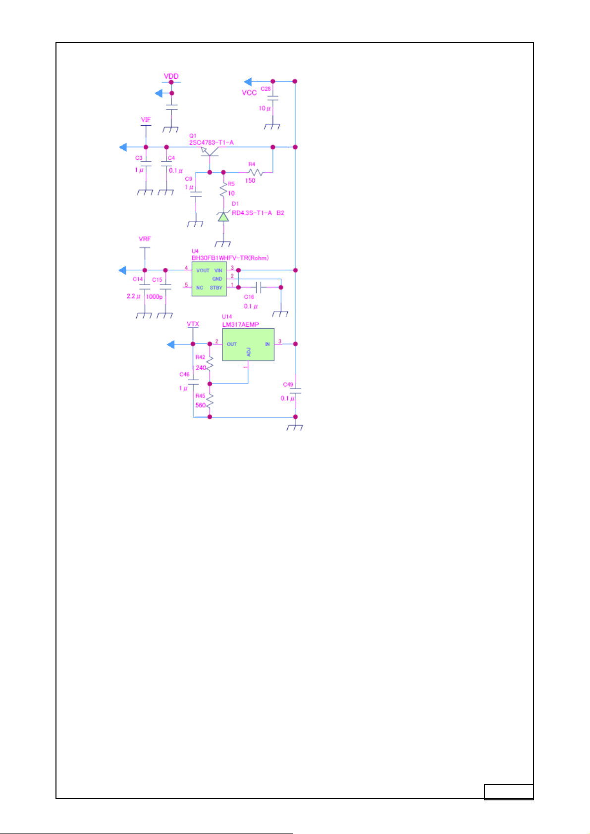
MMRW-MD-U01 uses five power supplies.
Vcc5V=U8 CPU farm wear write power voltage.
Vdd3.3V=U8 CPU internal, U5 power voltage, LED1-2 power voltage, U9 power voltage.
VIF3.5V=U1,U2,U3,U12,U15,U16,R1,VR1 power voltage.
VRF3V =U6 career oscillator, U11 PLL Synthesizer, U18 VCO, Q2, Q3 power voltage.
VTX3.8V=U19Transmitting circuit.
Page 10
10/20
Pin#
Name Signal Name I/O Type ACTIVE RESET Description
1
P0.1 RXD
I open-drain ? ? RF Rx
2
P0.0 RXD
I open-drain ? ? RF Rx
3
GND GND
- - - - GND
4
D+ D+
I/O - - - USB D+
5
D- D-
I/O - - - USB D-
6
VDD VDD
- - - - VDD(3.3V)
7
REGN POWER(VCC)
- - - - VCC(5V)
8
VBUS
USB/POWER(VCC) I - - - VCC(5V)
9
RST/C2CK RESET
O - - - Device Reset/C2CK
10
P3.0/C2D P3.0
O push-pull - H C2D
11
P2.3 TXSW
I open-drain L H RF Tx
12
P2.2 COP(+)/LBT
O open-drain H LBT sense(UHF only)
13
P2.1 LED2_G
O open-drain L L LED
14
P2.0 LED2_R
I open-drain L H LED
15
P1.7 COP(-)
O open-drain - H LBT sense(UHF only)
16
P1.6 DEBUG0
O push-pull - - Debug port
17
P1.5 ANTSW0
O open-drain H L Antenna SW (UHF only)
18
P1.4 ANTSW1
O open-drain H L Antenna SW (UHF only)
19
P1.3 PLL_LE
O push-pull H L Synthesizer control
20
P1.2 PLL_CLK
O push-pull H L Synthesizer control
21
P1.1 PLL_DAT
O push-pull H H Synthesizer control
22
P1.0 LED1_R
O open-drain L H LED
23 P0.7/VREF
LED1_G
O open-drain L H LED
24 P0.6/CNVSTR RFSW O push-pull L H LBT sense(UHF)
25 P0.5 UART_RXD I open-drain L H UART Rx
26 P0.4 UART_TXD O push-pull L H UART Tx
27 P0.3/XTAL2 Power_Change O push-pull H(Fix) H Output power control
28 P0.2/XTAL1 DEBUG1 O push-pull - - Debug port
7.4 Microprocessor’s pin assignment
7.5 RF antenna
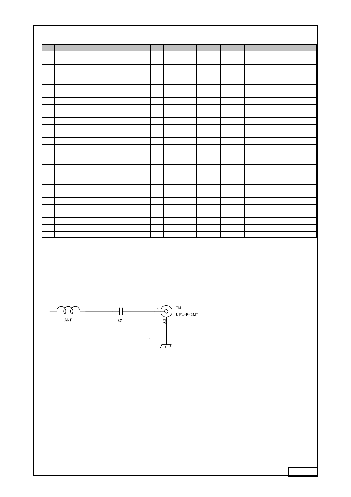
MMATU-OCA is 50Ω antenna connected to MMRW-MD-U01. The antenna prepares four types (866, 912, 923,
953). The antenna is a spiral antenna.
C1 = 1.5pF
Antenna connector = U.FL receptacle
C1 is used to adjust VSWR of the antenna.
Page 11
11/20
MMRW MCU
(C8051F321)
Frequency control
UART communication
(main.c)
USB communication
(usb.c)
Tag detection
(detect.c)
MMRW control
(command.c)
Read, Write, Lock
(rwcmd.c)
MM Chip
Receive response
(rfrcv.c)
Send command
(send.c)
UHF Frequency control
(pll.c)
Encryption / Decryption
(enc.c)
Command parser & Response reply
(main.c)
Listen Before
Talk
(LBT.c)
MMRW MCU
(C8051F321)
Frequency Synthesizer
(LMX2433)
Frequency control
(mmrw900.c)
Host
(PC or other micro controller)
USB
UART
Hardware
Hardware
Firmware
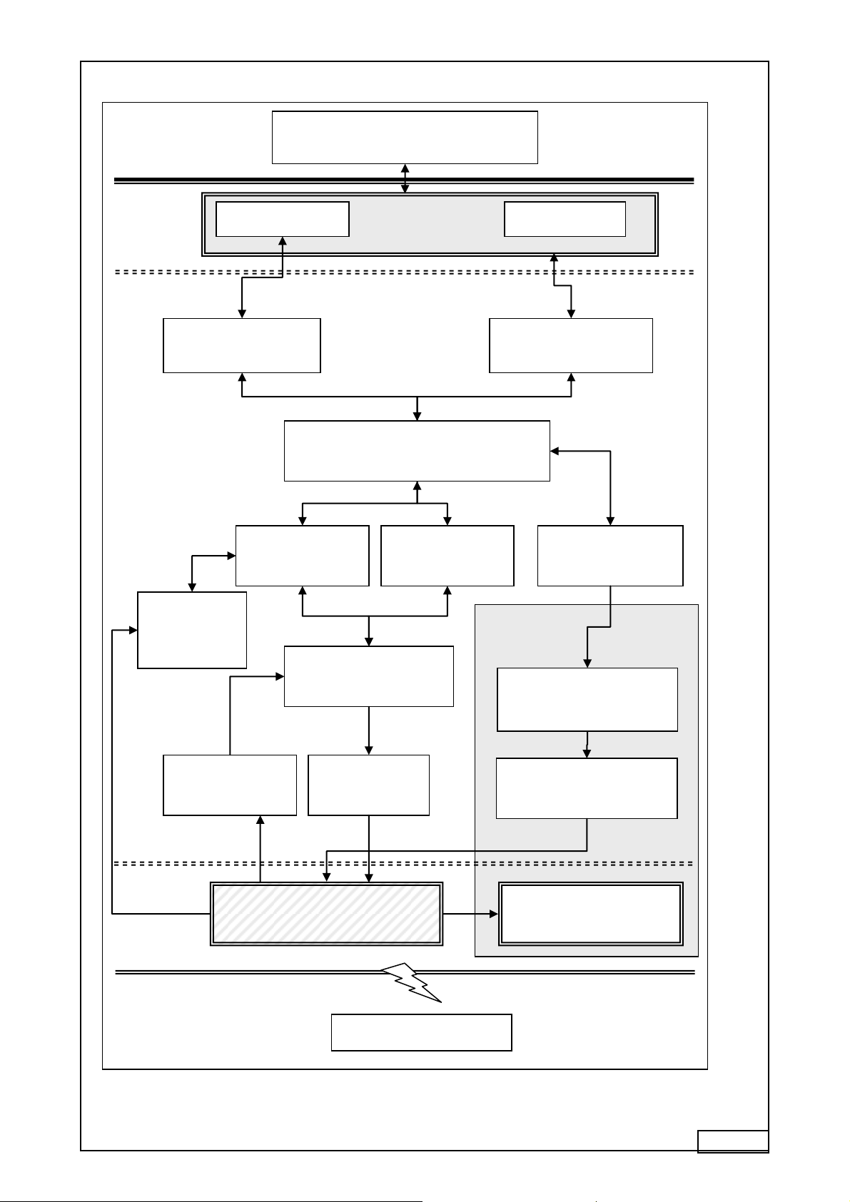
8 Firmware
The firmware was developed using “Keil C51 compiler” under Silicon Labs IDE. The firmware can be loaded into
the microcontroller using the “on-chip Silicon Labs 2-Wire (C2) debug interface” connected to a USB debug
Page 12
12/20
USB Debug Adaptor
PC
USB Cable
Completed Installation
adapter, driven by Silicon Labs IDE.
C8051F320.h contains the firmware specific C51 code. (Input, output pins, etc.).
The file mmrwmmrw900r.wsp is Silicon Labs IDE project file.
9 Firmware Writing Procedures
9.1 Firmware writing application start-up and installation
For firmware writing (OS: Windows XP SP2 or higher is recommended), double click「mcu_ide.exe」and follow
instructions on the screen accordingly.
http://www.silabs.com/products/mcu/Pages/SoftwareDownloads.aspx
“Start” “Silicon Laboratories” Select and start “Silicon Laboratories IDE”.
9.2 Firmware writing
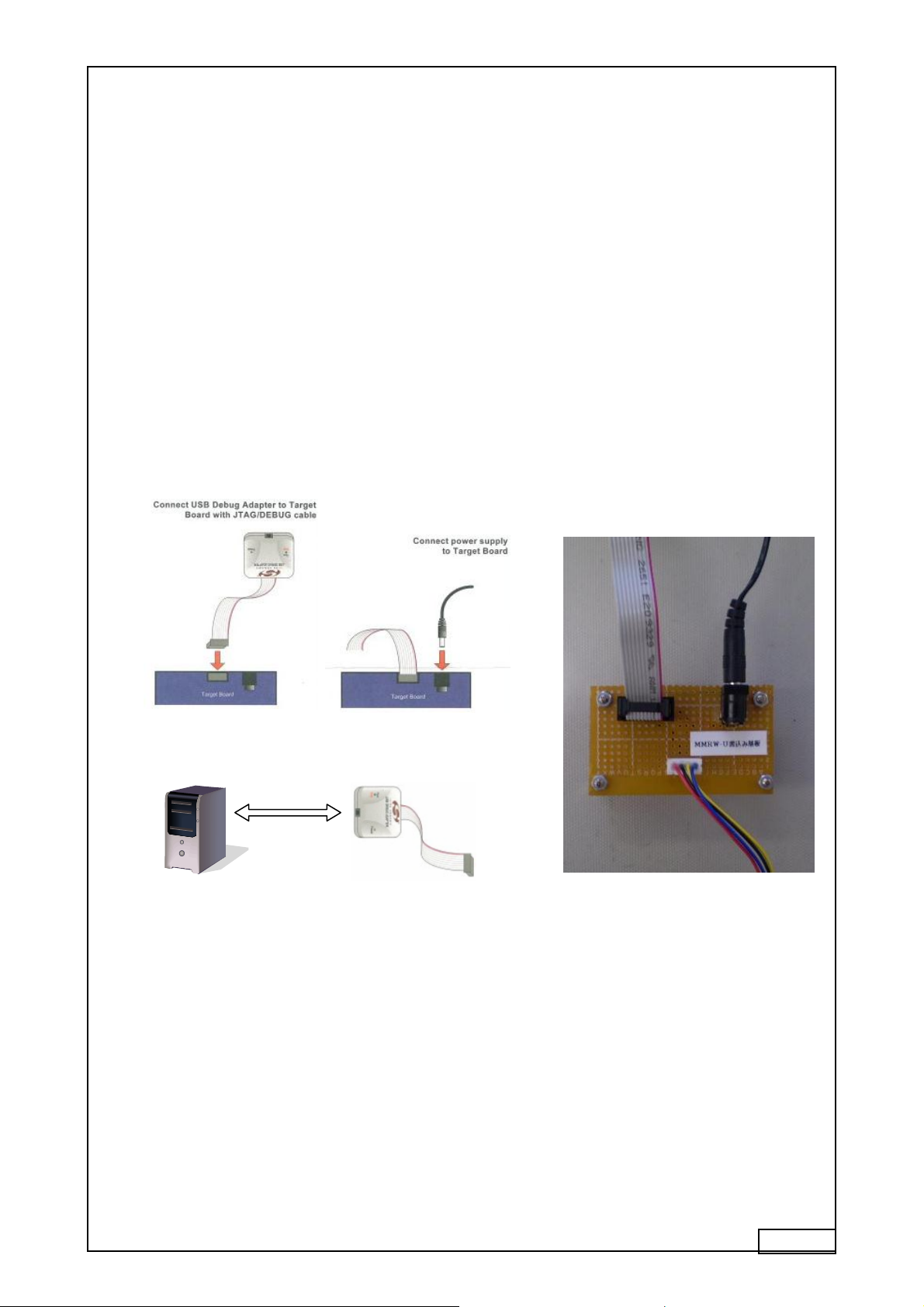
(1) Firmware file (MMRW-UHFver01.00.OMF) is saved in any folder in the PC used for firmware writing.
(2) USB Debug Adaptor and 5V-AC Adaptor are connected to MMRW-U writing substrate, and this debug
adaptor is connected to PC via USB cable.
Page 13
13/20
CN1
Connecting harness
Click
Connected correctly
Icon will be displayed
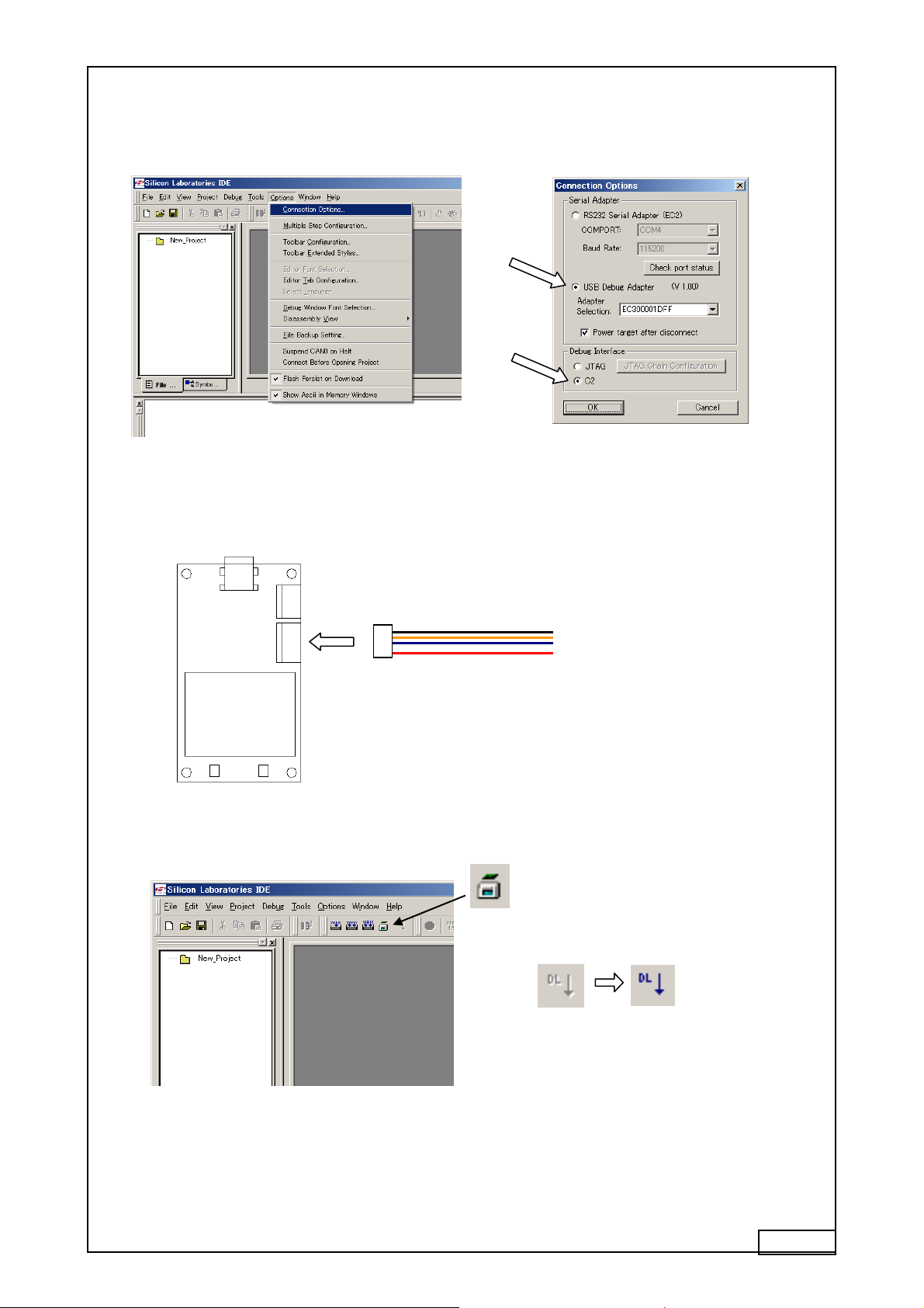
(3) Silicon Laboratories IDE starts.
(4) Set connection method for PC and connection substrate.
From the toolbar, select “Options” “Connection Options”, then set USB debug adaptor to connector.
(5) MMRW module is connected to “MMRW-U writing substrate”.
Harness for MMRW-U writing substrate is then connected to MMRW module CN1 (5 pin connector).
(6) PC and module connect electronically.
Page 14
14/20
“Flash Erased” is displayed when deleting succeed
Click
(Eg. Screen shows ORWI501.OMF saved in D:¥test)
Clicking “Browse” button then select is possible too
Click “Download” button
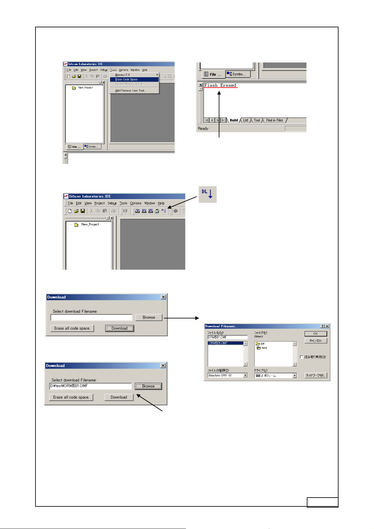
(7) In case where firmware has already been written, it is necessary to delete the firmware. If firmware is
newly written, delete procedure is unnecessary.
Select “Tools” ”Erase Code Space” from Toolbar, and erase firmware.
(8) Writing firmware into microcontroller.
Get started with below shown window, select the folder where firmware file (MMRW-UHF ver01.00
OMF) is saved, click “Download” button and thereby firmware writing starts.
Page 15
15/20
Green is displayed
Click
Normal disconnection
Icon will be disabled.
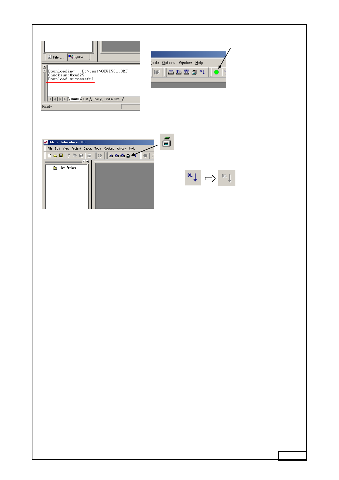
Once writing is succeed, below shown window will be displayed.
(9) PC and module electronically disconnected.
(10) MMRW module will detach from MMRW-U writing substrate.
Before module is detached, PC and module MUST follow procedure (9) for release.
Detach harness and therefore module is detached too.
Repeat (5) - (10) for the next firmware writing.
To end firmware writing, close the application.
Page 16
16/20
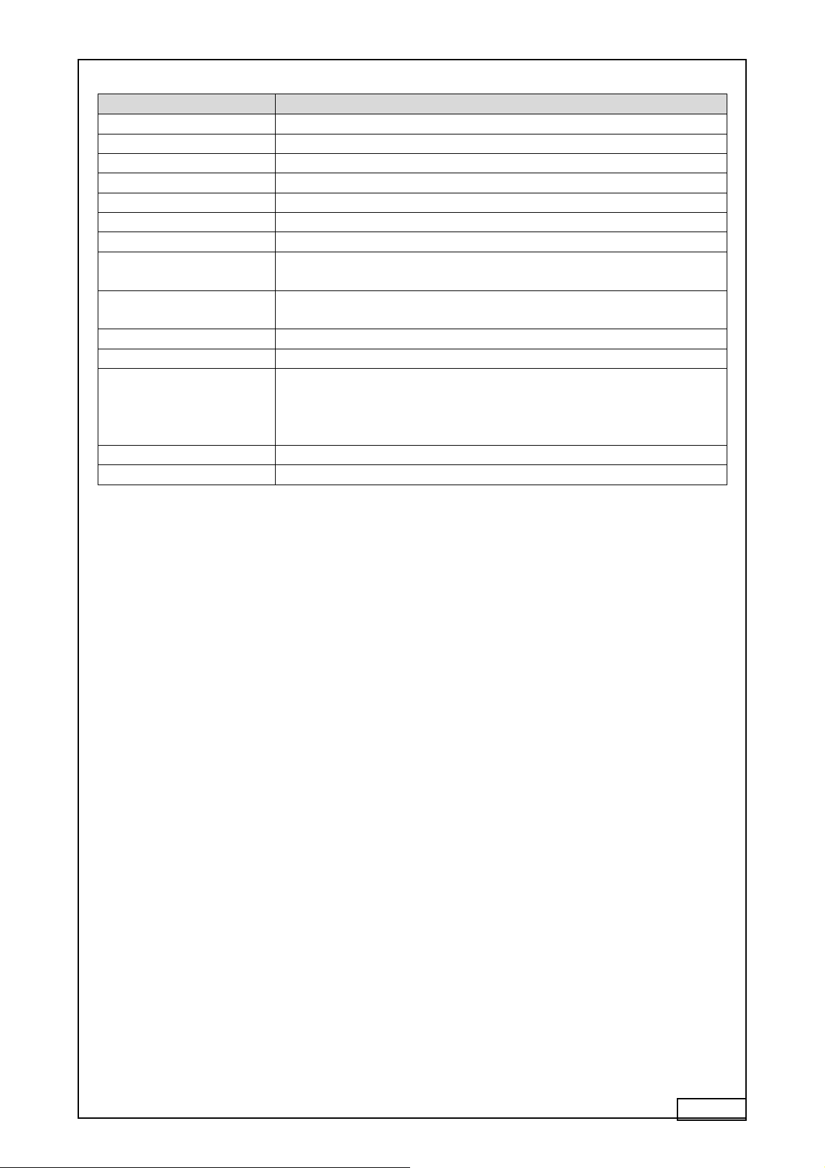
Items
Specification
Product number
MMRW-MD-U01
Appearance diagram
58(D) x 33(W) x 9.4(H) mm (Excluding surface bump’s presence)
Operation frequency
UHF
Communication standard
MM Chip original protocol communication
IC card/tag
IC card/tag with MM chip (Excluding on-chip antenna)
Modulation
Receive: ASK10% Transmit: 90%
Communication speed
Receive: 25Kbps Transmit: 40Kbps
Input power supply
DC5V (Power supply voltage variation: ±0.25V) (USB bus power supply /
external supply)
Current consumption
RF carrier ON: Approximately 430mA (Standard)
RF carrier OFF: Approximately 80mA (Standard)
RF output
Approximately 100mW
Antenna output impedance
50Ω
Temperature environment
Storage temperature range: -30ºC~+80ºC
Operation temperature range: -10ºC~+60ºC
Storage / operation humidity range: Below 90%RH (Non-condensation
situation)
Anti-collision
Unsupported
RF output I/F
2pin-ZH Connector/Side type SM4
10 Product general specification
Page 17
17/20
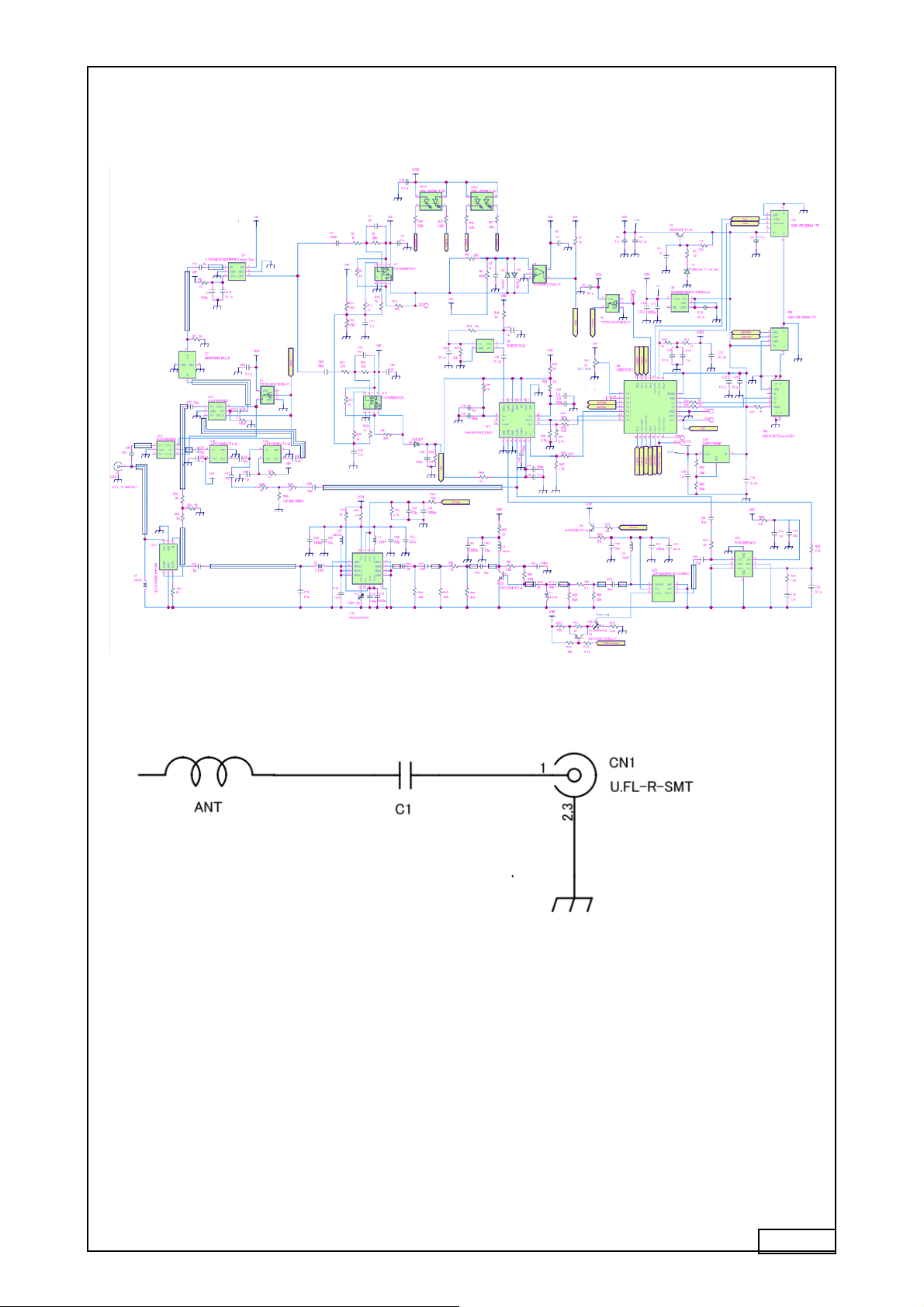
11 Annexes
11.1 Schematics
MMRW-MD-U01:
MMATU-OCA:
Page 18
18/20
Part Name
Specification
Qty
Part No.
RF Power Detector
1
U1
Comparator
1
U2
Dual Operational Amplifier
2
U3, 12
Regulator IC
1
U4 〃
1
U14
L-MOS 2
U5,9
TCXO 1
U6
B P for 915MHz
1
U7
MCU
16KB
1
U8
SPDT Switch
2
U10,13
Dual PLL IC
1
U11
Analog IC
2
U15,16
Hybrid Coupler
1
U17
Voltage-Controlled- Oscillator
1
U18
PA for GSM
1
U19
Variable Gain AMP
1
U20
Chip Resistor
1608 0Ω
2
R31,78
〃
1608 1Ω
1
R53
〃
1608 3.6Ω
1
R48 〃 1608 5.1Ω
1
R63 〃 1608 10Ω
6
R5,9,22,51,59,76
〃
1608 18Ω
4
R14,28,29,44
〃
1608 22Ω
2
R55,56
〃
1608 33Ω
3
R30,32,57
〃
1608 39Ω
2
R49,54
〃
1608 47Ω
2
R46,47
〃
1608 51Ω
3
R17,67,71
〃
1608 82Ω
1
R80 〃 1608 100Ω
2
R70,72
〃
1608 150Ω
4
R4,10,15,50
〃
1608 180Ω
3
R25,27,64
〃
1608 240Ω
1
R42 〃 1608 330Ω
5
R24,26,34,35,40
〃
1608 430Ω
2
R65,66
〃
1608 470Ω
1
R21
〃
1608 560Ω
1
R45 〃 1608 680Ω
1
R61 〃 1608 820Ω
2
R68,69
〃
1608 1KΩ
10
R1,2,7,11,12,18,19,33,,38,39
〃
1608 1.8KΩ
1
R62 〃 1608 2.7KΩ
3
R36,37,43
〃
1608 4.7KΩ
3
R52,58,74
〃
1608 5.6KΩ
1
R60 〃 1608 10KΩ
4
R16,20,73,79
〃
1608 30KΩ
4
R3,13,23,41
〃
1608 33KΩ
1
R6
Chip Resistor
1608 620KΩ
1
R8
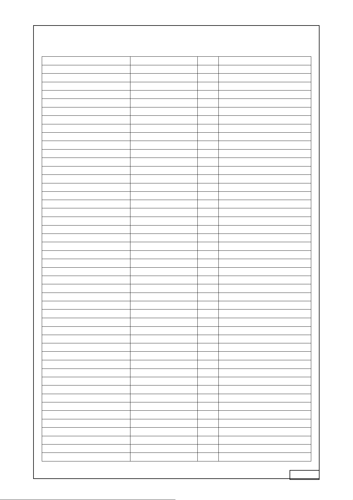
11.2 List of components
MMRW-MD-U01
Page 19
19/20
〃
1608 560KΩ
1
R77 〃 1608 1MΩ
1
R75
Variable Resistance
Surface Mount 1KΩ
2
VR1,2
Chip Capacitor
1608 3pF
2
C1,70
〃
1608 5.6pF
1
C74
〃
1608 6pF
1
C10 〃 1608 7pF
1
C2 〃 1608 10pF
8
C38,42,47,50,65,66,67,68
〃
1608 33pF
14
C31,33,37,41,51,53,55,56,
C59,60,63,64,71,72
〃
1608 56pF
1
C26
〃
1608 100pF
8
C12,30,34,39,44,69,78,80
〃
1608 180pF
1
C6 〃 1608 1000pF
6
C15,52,58,61,62,79
〃
1608 0.1μF
14
C4,5,11,13,16,19,20,21,22,
C24,25,27,49,73
〃
1608 1μF
17
C3,7,8,9,17,18,23,29,32,35,
C40,43,45,46,48,54,76
〃
1608 2.2μF
1
C81 〃 2125 2.2μF
2
C14,57
Trimming Capacitor
Surface Mount
1
C77
〃
3216 10μF
1
C28
Chip Coil
1608 2.7nH
1
L5
〃
1608 4.7nH
1
L7 〃 1608 10nH
3
L1,2,6
〃
1608 15nH
2
L3,4
Transistor
Surface Mount
2
Q1,Q4
〃
Surface Mount
1
Q2
〃
Surface Mount
1
Q3
Diode
Surface Mount
3
D2,3,4,
Zener Diode
Surface Mount
1
D1
LED
Surface Mount
2
LED1,2
Connector
Surface Mount
1
CN1
〃
Surface Mount
1
CN2
Mini USB Connector
Surface Mount
1
CN3
Coaxial Connector
Surface Mount
1
CN4
Shield Case A
Component Side
1
Shield Case B
Solder Side
1
R/F Substrate (Four-layered)
58 x 33 x 1mm
1
S/No. Sticker
4 x 19mm
1
Part Name
Specification
Qty
Part No.
Antenna Substrate
7.6x9.64x1.6mm
1
RoHS compliance
Capacitor
1.5pF
1
C1
Connector
U.FL receptacle
1
CN1(RS:426-5469)
MMATU-OCA
Page 20
20/20
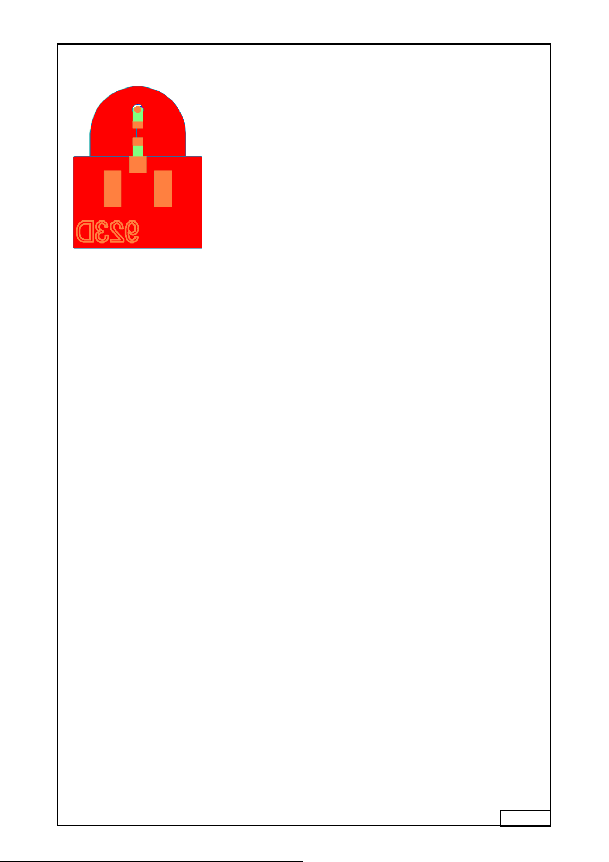
11.3 Antenna layout
12 FCC STATEMENT
THIS DEVICE COMPLIES WITH PART 15 OF THE FCC RULES. OPERATION IS SUBJECT TO THE
FOLLOWING TWO CONDITIONS: (1) THIS DEVICE MAY NOT CAUSE HARMFUL INTERFERENCE,
AND (2) THIS DEVICE MUST ACCEPT ANY INTERFERENCE RECEIVED, INCLUDING
INTERFERENCE THAT MAY CAUSE UNDESIRED OPERATION.
NOTE: This equipment has been tested and found to comply with the limits for a Class B digital device, pursuant
to part 15 of the FCC Rules. These limits are designed to provide reasonable protection against harmful
interference in a residential installation. This equipment generates, uses and can radiate radio frequency energy
and, if not installed and used in accordance with the instructions, may cause harmful interference to radio
communications. However, there is no guarantee that interference will not occur in a particular installation. If
this equipment does cause harmful interference to radio or television reception, which can be determined by
turning the equipment off and on, the user is encouraged to try to correct the interference by one or more of the
following measures:
- Reorient or relocate the receiving antenna.
- Increase the separation between the equipment and receiver.
-Connect the equipment into an outlet on a circuit different from that to which the receiver is connected.
-Consult the dealer or an experienced radio/TV technician for help.
 Loading...