

ZMD31050
Advanced Differential Sensor Signal Conditioner
Application Note PRELIMINARY
1. Startup
First you have to install driver and software form CD - refer KIT2 installation description
“CB_descr_*.pdf” (former name “tech_desr_comm._board_revxxx.pdf”) in folder “Manual Evaluation Kit
2.0” on CD for details.
For a demo application without hardware access it is not necessary to install the USB port driver. After
the end of software installation procedure you find two additional icons on your desktop or programs in
program menu:
• ZMD31050 (former ZMD31050 EV KIT)
• ZMD31050_SSC2 (former ZMD31050 EV KIT2)
ZMD31050 is tool supporting all features and functions in detail – recommended for being familiar with
the ZMD31050, design in a sensor, developing and verifying a configuration/application.
ZMD31050_SSC2 is tool, which is made for pre series calibration work. The configuration is displayed
as configuration words only, but this tool supports “ZMD SSC Kit command language” (SSC_CML).
SSC_CML enables to write command procedures for full automated calibration of sensor modules.
SSC_CML is in development now. Additional ZMD31050_SSC2 software enables mass calibration
using “ZMD SSC Mass Calibration Board” – a mass calibration solution, which calibrates up to 120
sensor modules in one batch.
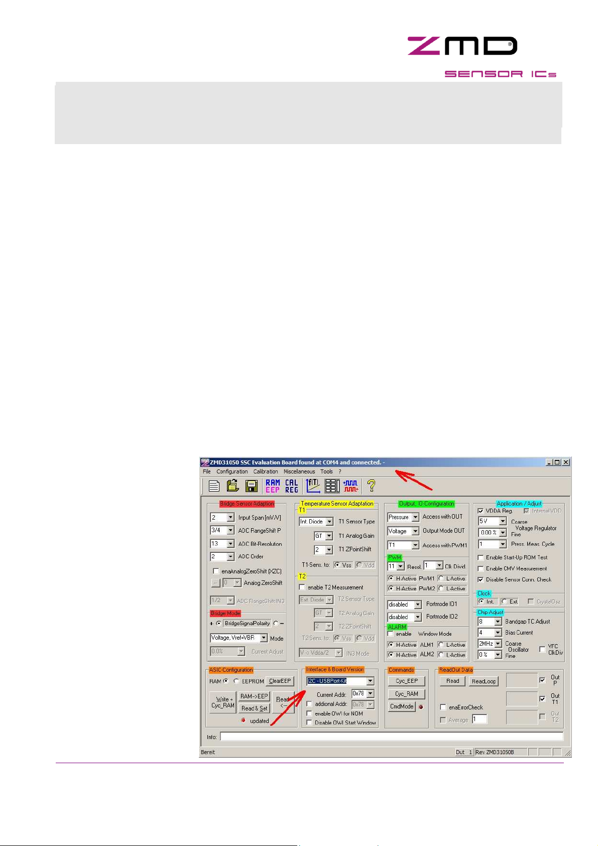
1.1 ZMD31050 software
After starting ZMD31050
software has to be select
desired interface (lower
arrow).
ZMD31050 software is
applicable for KIT1 (in
software called
“ParallelPort-Kit”) and
KIT2 (“USBPort-Kit”).
ZMD recommends for first
steps I2C interface.
Founded hardware and
port is messaged in top of
the window, if
“Communication Board”
and “ZMD31050 SSC
Board” is connected at
the computer and was
found by the software
(upper arrow). ZMD31050
circuit revision number is
displayed in status line.
Copyright © 2005, ZMD AG, 2005-05-17
All rights reserved. The material contained herein may not be reproduced, adapted, merged, translated, stored, or used without the prior
written consent of the copyright owner. The Information furnished in this publication is preliminary and subject to changes without notice.
1/8
ZMD31050
Advanced Differential Sensor Signal Conditioner
Application Note PRELIMINARY
To change type of interface select first “NULL” and then a new one. To verify command mode press
“CmdMode” button, if applicable the “LED” near the “CmdMode” button is flashing green for some
seconds.
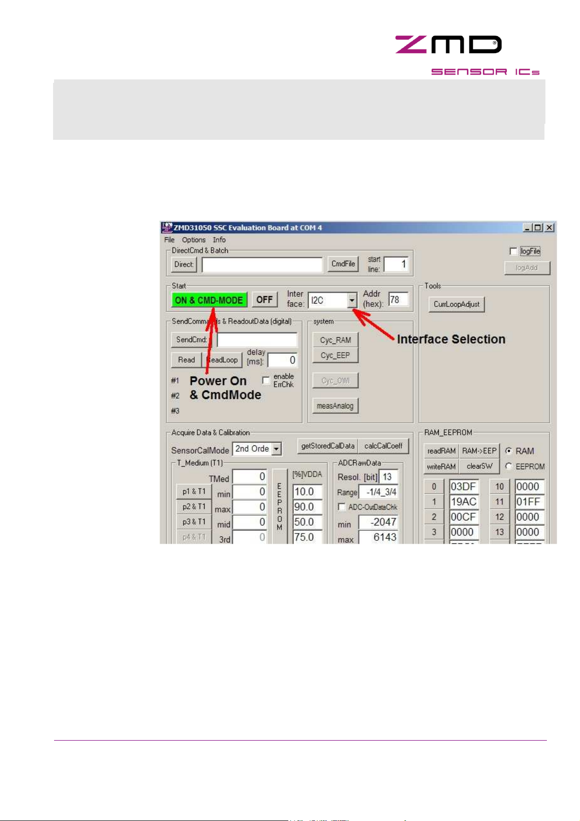
1.2 ZMD31050_SSC software
ZMD31050_SSC
software supports
only KIT2 (USB).
After starting
ZMD31050_SSC
software
connection status
is displayed in
header of window.
To access
ZMD31050 has to
be select desired
interface and then
power on.
Supply LED on
SSC Board is
flashing, if this
successful and
indicates, that
ZMD31050 IC is
supplied correct.
As next step
current register
content can be
read out by
pressing the “readRAM” button in RAM_EEPROM frame. RAM content is displayed then RAM register
fields #1...31.
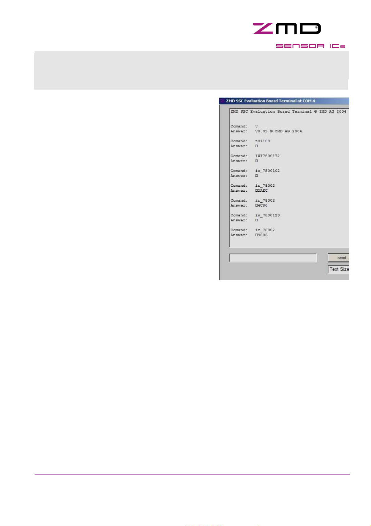
1.3 ZMD SSC Terminal
ZMD SSC terminal is the lowest level of communication, which transfers commands direct to
communication board (CB) microcontroller. Controller command language is used for this and is
described in “CB_descr_*.pdf” chapter 7 & 8.
Input a command in input line and press <CR> or “send”. Sent command and answer is displayed in
terminal window. A practical communication example is displayed terminal program screenshot.
Copyright © 2005, ZMD AG, 2005-05-17
All rights reserved. The material contained herein may not be reproduced, adapted, merged, translated, stored, or used without the prior
written consent of the copyright owner. The Information furnished in this publication is preliminary and subject to changes without notice.
2/8
ZMD31050
Advanced Differential Sensor Signal Conditioner
Application Note PRELIMINARY
T01100 set trigger, communication should start
100ms after power on
IWT7800172 I2C, power on & send cmd: "72"
= activate ZMD31050 command mode
IW_7800102 I2C, send cmd: "02" = start cylce ram
IR_78002 I2C, read 2 bytes of SIF output register
=> 0x2AEC digital readout result of conditioning
change adjustment of potentiometer on sensor
replacement board now => changed input signal
IR_78002 I2C, read 2 bytes of SIF output register
=> 0x4C80 digital readout result of conditioning
changed input signal delivers also other output signal
IW_7800129 I2C, send cmd: "29"
= read content fof RAM register 0x19
content of addressed register is copied to SIF output,
continuous conditioning (“cycle_ram”) is stopped
IR_78002 I2C, read 2 bytes of SIF output register
=> 0x9806 register content of RAM register 0x19
ZMC SSC Terminal
1.4 Troubleshooting
Communication problems:
• If software don’t found the communication board check in “system control” of your computer for
accessible COM ports etc. – refer “CB_descr_*.pdf” for details)
• If software get no access to ZMD31050 (e.g. message “… Command Mode failed …”) verify power
supply of the ZMD31050 (wrapped jumpers, measure supply voltage @ K10 Vsupply-GND, …).
Software can detect type of connected SSC board - in headline of software type of founded SSC
board is messaged. Verify board type …
• Try it again with other software (ZMD31050_SSC2.exe).
• A error code is displayed in case of communication errors in software. ZMD31050_SSC2 messages
errors in “SendCommand & ReadoutData” frame. An error code is an “e” with a number of three
digits e.g. “e032”. Refer “tech_desr_comm._board_revxxx.pdf” for detailed error description. At
using ZMD31050-software press “Read” button in “ReadOut Data” frame of main window “ or open
“RAM-Register” dialogue (RAM_EEP-icon) and press also “Read” button. Error code is displayed
in related output data fields.
• If all this doesn’t help send problem description with screenshots of software, software version
(about dialogue), error code etc. to ZMD support. Use mail task in about/support dialogue for this.
Copyright © 2005, ZMD AG, 2005-05-17
All rights reserved. The material contained herein may not be reproduced, adapted, merged, translated, stored, or used without the prior
written consent of the copyright owner. The Information furnished in this publication is preliminary and subject to changes without notice.
3/8

ZMD31050
Advanced Differential Sensor Signal Conditioner
Application Note PRELIMINARY
2. First Example
The following example describes first
steps being familiar with KIT2 and
ZMD31050-software and ZMD31050.
• Plug all 3 delivered PCBs in order
Communication Board (CB) –
Sensor Signal Conditioner Board
(SSC) - Sensor Replacement Board
(SR) together and connect these to
the USB port of your computer
• Verify wrapped jumper connection
at SSC: K5 (Vsupply), K10 (Bridge
Mode Voltage) and at SR: K4 (BR)
• Start ZMD31050 software and
activate USB Port access via I2C
interface (refer chapter 1.1) and
verify accessed board and
command mode
• Open File menu and load
“31050_kit_default.31050” configuration. These file contains needed programming data for
ZMD31050 circuit to adjust/configure the ZMD31050 for application completely. These file or set of
data is called following “config”.
Loading a saved configuration
“31050_kit2_default.31050” config is loaded in software now.
These config is made for KIT2 to learn basics in handling of
KIT and ZMD31050. A short description of the loaded config
is displayed as info text. These config gain the input signal generated by the sensor replacement (SR) and was
calibrated to deliver 0.5/4.5V for SR potentiometer top/down
end adjustment. To verify this you have to do:
• Connect a DMM to the analog out of the ZMD31050. Use
“SSC: K10 – pin OUT“ and “SSC: K10 – pin GND”
measure point for this. Now the DMM measures the
analog output signal (VOUT). Refer ZMD31050 SSC
Board description for details.
Write to 31050 and starting a config
• Adjust SR – potentiometer (poti) in middle position.
• Press “Write+Cyc_RAM” button: Loaded config is written
(Write) to ZMD31050 and started (Cyc_RAM) now.
• Check measured VOUT at the DMM: VOUT should be
approx. 2.5V and should be alter at changing SR – poti
adjustment.
• Measure VOUT for top and bottom position of the poti.
Copyright © 2005, ZMD AG, 2005-05-17
All rights reserved. The material contained herein may not be reproduced, adapted, merged, translated, stored, or used without the prior
written consent of the copyright owner. The Information furnished in this publication is preliminary and subject to changes without notice.
Open “Sensor calibration“ dialogue
4/8

ZMD31050
Advanced Differential Sensor Signal Conditioner
Application Note PRELIMINARY
These values should be 0.5/4.5V. In most cases this wouldn’t be so and is caused by tolerances of all
components/elements at the PCBs – calibration is necessary. This is the next step.
• Open “Sensor-Calibration” dialogue (last picture)
• A two point calibration
(poti top & down) should be
done.
“Calibration Mode” is
linear, no temperature
behaviour. Adjust this like
displayed in screenshot.
Tooltips in software give
you additional help for use.
“Targets” are the output
aims for calibration. In
example output voltage
should be 0.5/4.5V for
minimum/maximum input
signal. All targets are
inputted proportionally to
VDDA, complete calibration
is done proportionally to
VDDA. For VDDA=5V is a
required output voltage of 0.5/4.5V => target is 10/90%. This has to be inputted in target frame for
minimum and maximum.
“Acquire Raw Data” frame is used to collect data of all
needed measurement points for calibration. In minimum 2
input fields and acquire buttons are enabled depending on
selected “Calibration Mode”.
Sensor-Calibration: Target input fields and acquire raw data buttons
• Adjust SR poti to top end and press “P1M” button.
The current analogue input signal is gained and AD-converted
now, the result is displayed in the input field beside the button.
• Adjust SR poti to down end and press “P2M” button.
Both required data points for calibration are acquired now,
calculation of calibration coefficients can be done now.
Calibration results
• Press “calcCoeff” button in “Sensor Calibration” dialogue.
Software messages success of coefficients calculation.
Founded calibration coefficients are copied to RAM register
block. To verify this open “RAM-Register” dialogue by
pressing the “RAM_EEP” icon in icon list of software.
• Press “Write+Cyc_RAM” button in main window now.
Calibration results are transferred to ZMD31050 and activated
Copyright © 2005, ZMD AG, 2005-05-17
All rights reserved. The material contained herein may not be reproduced, adapted, merged, translated, stored, or used without the prior
written consent of the copyright owner. The Information furnished in this publication is preliminary and subject to changes without notice.
RAM Register dialogue
5/8

ZMD31050
Advanced Differential Sensor Signal Conditioner
Application Note PRELIMINARY
now. New calibration is ready and result can be verified now.
• Measure VOUT for top and bottom position of the poti.
You should measure 0.5V for poti down end 4.5V for poti top end now.
• Repeat the same procedure with reverse acquiring (pressing P2M instead P1M and otherwise).
You will get a mirrored output function for this case. We see, the output signal can be inverted by
calibration for the same input signal.
3. ZMD31050 Software Description
Main window is split in 8 frames:
• “ASIC-Configuration” configures memory access. Configuration data can be written into RAM or
EEPROM. All modifications can be done in and activated from RAM. Write new configuration into
EEPROM, if changes should be made non-volatile. To do this, ZMD recommends to write first all
data into RAM and then copy into EEPROM by pressing “RAM->EEP” button. The “LED” indicates
whether the displayed information in software are identical to ZMD31050 circuit or not.
• “Bridge Sensor Adaptation” enables config of basic “Sensor Design-In” and “ADC” parameters
• “Temperature Sensor Adaptation” enables configuration of temperature measurement for
conditioning (T1) and additional temperature measurement
• “Output, IO-Configuration” configures analogue and PWM output and IO channel
• “Application/Adjust” configures supply voltage regulator, safety feature, bandgap voltage and TC.
Additional clock frequency and biasing can be adapted/modified.
• “Interface & Board Version” is used to select interface type, board and addressing.
• “Commands” enables to start signal conditioning using RAM or EEPROM data. Enabled
“Command Mode” can be verified and is displayed by a green flashing “LED”.
• “ReadOut Data” enables digital readout via serial communication interface (SIF). If continuous
readout is activated averaging mode can be enabled. Via the SIF can be read output data for
pressure and temperature 1 & 2 channel. A description of data is displayed beside the output fields.
Info line enables to add a short description of application to configuration data. Additional in status line
is displayed revision number of accessed ZMD31050 circuit. Refer detailed software description for
further information and examples.
Copyright © 2005, ZMD AG, 2005-05-17
All rights reserved. The material contained herein may not be reproduced, adapted, merged, translated, stored, or used without the prior
written consent of the copyright owner. The Information furnished in this publication is preliminary and subject to changes without notice.
6/8

ZMD31050
Advanced Differential Sensor Signal Conditioner
Application Note PRELIMINARY
4. Calibration Examples
4.1 Conditioning a Pressure Signal
4.2 Conditioning a Temperature Signal
4.3
1st step - acquire calibration data
temperature out calibration target:
• 0.5V at 0deg = 10%
• 4.5V at 100deg = 90%
and/or digital:
• 3277 (10% of 32768) at 0deg
• 29491 (90% of 32768) at 100deg
--- room temperature = 25deg
Temperature-Calibration Example
OW_78001D9 => acquiring T1
OR_78002 => you get first acquired raw data for current temperature calibration point now (1) in example: 1000
--- change of temperature =50deg
OW_78001D9 => acquiring T1
OR_78002 => you get second acquired raw data for current temperature calibration point now (2) in example: 2000
=> calculate coefficients now and write calibration data to RAM/EEPROM
OW_7800102 => start cycle RAM
OR_78004 => readout of 4 bytes, @ 25deg you should read 9830
Copyright © 2005, ZMD AG, 2005-05-17
All rights reserved. The material contained herein may not be reproduced, adapted, merged, translated, stored, or used without the prior
written consent of the copyright owner. The Information furnished in this publication is preliminary and subject to changes without notice.
7/8

ZMD31050
Advanced Differential Sensor Signal Conditioner
Application Note PRELIMINARY
The information furnished here by ZMD is believed to be correct and accurate. However, ZMD shall not be liable
to any licensee or third party for any damages, including, but not limited to, personal injury, property damage, loss
of profits, loss of use, interruption of business or indirect, special, incidental, or consequential damages of any
kind in connection with or arising out of the furnishing, performance, or use of this technical data. No obligation or
liability to any licensee or third party shall result from ZMD’s rendering of technical or other services.
For further
information:
ZMD Stuttgart Office
Nord-West-Ring 34
70974 Filderstadt - Bernhausen
Tel.: +49 (0)711.674.517-0
Fax: +49 (0)711.674.517-99
sales@zmd.de
www.zmd.biz
ZMD AG
Grenzstrasse 28
01109 Dresden, Germany
Tel.: +49 (0)351.8822.310
Fax: +49 (0)351.8822.337
sales@zmd.de
www.zmd.biz
ZMD America Inc.
201 Old Country Road, Suite 204
Melville, NY 11747
Tel.: (631) 549-2666
Fax: (631) 549-2882
sensors@zmda.com
www.zmd.biz
Copyright © 2005, ZMD AG, 2005-05-17
All rights reserved. The material contained herein may not be reproduced, adapted, merged, translated, stored, or used without the prior
written consent of the copyright owner. The Information furnished in this publication is preliminary and subject to changes without notice.
8/8
 Loading...