

Sennheiser DRM 85,DRM 85-C Service Manual
SA 070931
Subject to alterations
Sennheiser electronic GmbH & Co. KG • 30900 Wedemark
Phone: +49 (5130) 600 0 • Fax: +49 (5130) 600 300 1/41
DRM 85
DRM 85-C
Service manual
Short description
The Digital Recording Microphone is based on traditional microphone
techniques in order to achieve excellent acquisition performance. It includes
embedded recorder functionalities, that stores the digitized audio data
to a 1 GByte NAND Flash Memory.
The USB port can be used to download the audio data to a PC with a standard
browser as well to upload configuration data from PC to the DRM. Two AA
mignon alkaline batteries provide about 7 hours continous power.
Features
• Omni-directional condenser capsule at DRM 85,
cardioid condenser capsule at DRM 85C
• Pre-record buffer 0 to 10 seconds
• Digital / Analog converter
• DC/DC converter
DRM 85-C, DRM 85
2/41 09/2007
Safety requirements
Observe safety regulations.
Observe ESD instructions while handling electrostatically endangered components.
Only skilled persons are allowed to alter and repair. For repairs and exchanges only
approved components according to the current spare parts list are allowed.
For safety and certification reasons it is forbidden to alter the product without
authorization. Otherwise, the person who has altered the product is liable for any
consequential damage.
repairs/exchanges The following instructions for overhaul and testing must be followed.
In case of unusual problems please contact your Sennheiser distributor.
CAUTION
During SMD component soldering you may
destroy them by using a standard soldering
iron for several seconds.
Only use adapted soldering tools when
soldering SMD components.
SMD

DRM 85-C, DRM 85
09/2007 3/41
Contents
1 Controls and indicators..................................................................................4
2 Specifications..................................................................................................5
3 Description ......................................................................................................7
3.1 Mechanical design ................................................................................................ 7
3.2 Electrical design .................................................................................................... 7
3.3 Functional description ......................................................................................... 7
3.4 Disassembly.........................................................................................................14
3.5 Assembly..............................................................................................................21
3.6 Firmware including updates............................................................................. 24
3.7 Known faults .......................................................................................................25
4 Exploded view.............................................................................................. 26
5 Test and alignment instructions ............................................................... 28
5.1 Measuring set-up................................................................................................ 28
5.2 Test table .............................................................................................................29
6 Circuit diagrams........................................................................................... 31
Block diagram...................................................................................................................31
AF board, circuit diagram...............................................................................................32
AF board, printed circuit board, component side......................................................33
AF board, printed circuit board, solder side................................................................ 33
Connector board, circuit diagram .................................................................................34
Connector board, printed circuit board, solder side..................................................35
Connector board, printed circuit board, component side ........................................ 35
Keyboard PCB, circuit diagram ...................................................................................... 36
Keyboard PCB, printed circuit board, component side............................................. 36
Keyboard PCB, printed circuit board, solder side.......................................................36
Processor board, circuit diagram, part 1/3.................................................................37
Processor board, circuit diagram, part 2/3.................................................................38
Processor board, circuit diagram, part 3/3.................................................................39
Processor board, printed circuit board, component side ......................................... 40
Processor board, printed circuit board, solder side................................................... 41
DRM 85-C, DRM 85
4/41 09/2007
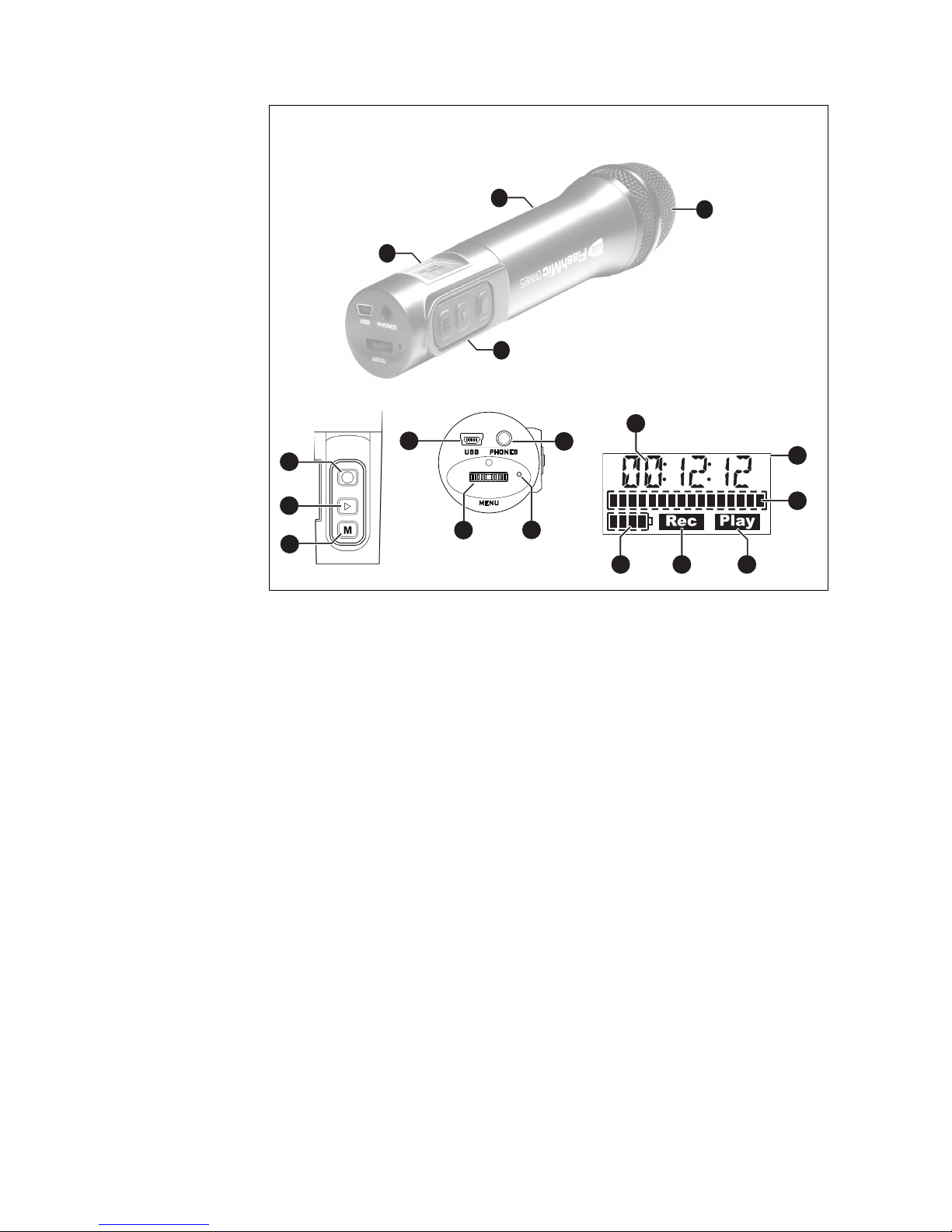
1 Controls and indicators
쐃 LC display
쐇 FlashMic body
쐋 Protective basket (windshield) over mic capsule
쐏 Main operating control section
쐄 REC button [쎲]
쐂 PLAY button [왘]
쐆 MENU/STOP button [M]
쐊 Multi-function jogswitch control
쐎 USB connector (5 pin Mini-B)
쐅 PHONES: monitor output (3.5 mm 3-pole jack socket)
쐈 Record mode LED (REC LED)
쐉 6-character alphanumeric display
씈 Display backlight
씉 16-segment bargraph meter -
provides an indication of recording and playback level
씊 “PLAY“ - indicates FlashMic is in replay mode
씋 “REC“ - indicates FlashMic is in record mode
씌 4-segment battery status indicator
3
2
1
4
11
10
9
8
7
6
5
12
17 16 15
14
13
Display window

DRM 85-C, DRM 85
09/2007 5/41
2 Specifications
Sampling frequency ___________________48 kHz, 44.1 kHz or 32 kHz;
selection with FlashMic Manager
software or DRM 85 directly.
Bit resolution (linear) __________________16 Bit
Audio formats _______________________linear PCM or MPEG 1 layer 2;
selection with FlashMic Manager
software or DRM 85.6 mode settings
Bit rate (MPEG) _______________________192 kbps, 160 kbps or 128 kbps
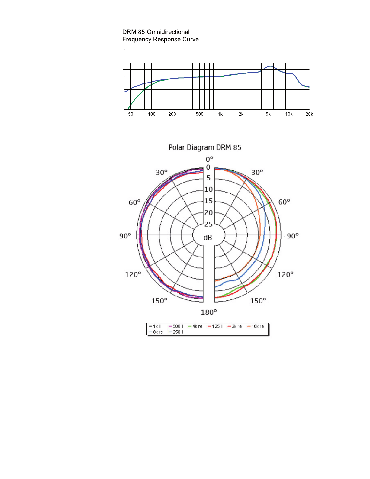
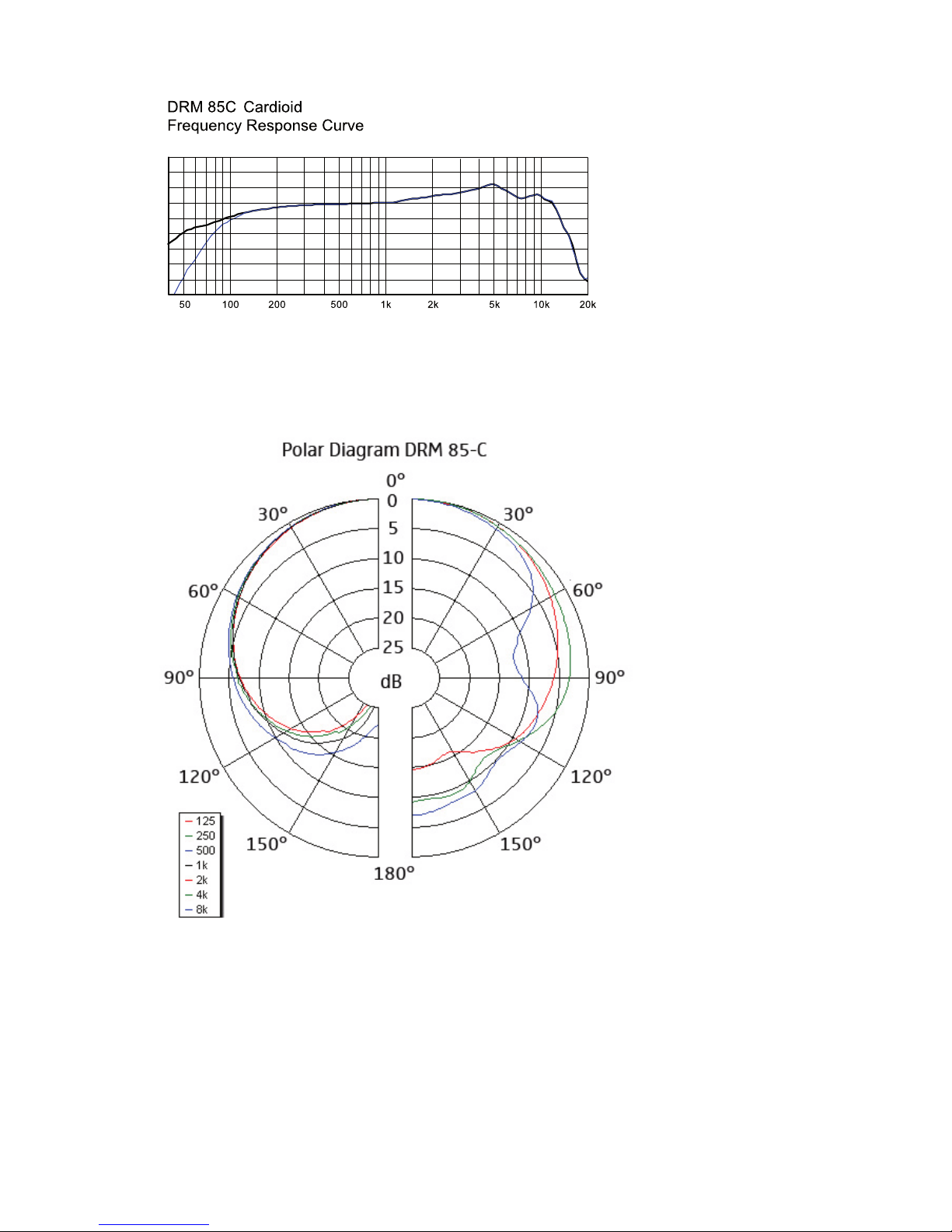
Frequency response (recorder)
without capsule _________________20 Hz to 20 kHz ± 1 dB
at 48 kHz FS Linear PCM
with capsule ____________________see measured frequency response
curves, page 11ff
THD + N ____________________________< 0.1% (20 Hz to 20 kHz)
at 48 kHz FS linear PCM
Number of channels ___________________1 (mono)
Microphone capsule ___________________
DRM 85 ________________________omni-directional,
DRM 85C _______________________cardioid
Record level _________________________automatic gain control (AGC = on);
manual gain control (AGC = off)
High pass filter _______________________switchable on/off;
12 dB/octave at 100 Hz
Data storage system __________________fixed internal NAND flash memory;
capacity 1 GB.
Date / Time _________________________internal real-time clock, running as
long as power supply is available.
back-up supply for 1 minute to allow
battery change. set / synchronized
by host computer application
according to host computer clock.
manual setting on DRM 85 by menu
item.
File format __________________________broadcast wave file (.wav). linear
PCM or MPEG 1 layer 2 compressed.
date / time stamp is stored in file
header. Filename generated
automatically by DRM 85, basic text
string provided from PC software.

DRM 85-C, DRM 85
6/41 09/2007
File system _________________________ FAT 16, cluster size 32 kB. mounts as
a removable drive via USB mass
storage device protocol. file transfer
is possible with the FlashMic
Manager software or through
Windows Explorer and Mac OS
finder.
Headphone output ___________________ 3.5 mm stereo socket, mono signal
to both channels. manual volume
control by rotary switch. output may
be used for audio recording on PC.
load impedance for 32 Ω
USB interface ________________________ USB 2.0 compliant interface with
“Full Speed” (12 Mbit/s max.)
transmission speed
connector type “Mini B”, 5 pin
User presets ________________________ Up to 9 presets in a preset.cfg file,
uploaded from host computer,
selected by menu item on DRM 85
Pre-record __________________________ off/ on, up to 10 sec in 1 sec step,
configured with FlashMic Manager
application on host computer
Nominal supply voltage ________________ 3 V
DC
Operating voltage ____________________ 2 V
DC
to 3 V
DC
Current consumption
at nominal voltage _______________ approx. 175 mA
Battery ____________________________ 2 x mignon AA; per 1.5 V
DC
Low Bat switch-off threshold
with batteries __________________ +1.8 V
DC
with accu ______________________ +1.9 V
DC
Operating time ______________________ about 7 hrs with Varta blue batteries
or Panasonic 2000 mAh Accu
Weight ____________________________ 366 grams (without batteries)
Dimensions _________________________ length 244 mm / 9.6 inches.
diameter at widest point
(mic capsule) 50 mm, 2 inches.
Record
mode
Audio format Sample
rates
Bit rates Recording time
hours
(theoretical)
Recording time
hours
(displayed)
LIN48K Linear PCM 48 kHz 768 kbps 3 hrs 6 min 3 hrs 4 min
LIN44K
Linear PCM 44,1 kHz 705.6 kbps 3 hrs 22 min 3 hrs 20 min
LIN32K
Linear PCM 32 kHz 512 kbps 4 hrs 39 min 4 hrs 36 min
MP48k
MPEG1 Layer 2 48 kHz 192 kbps 12 hrs 25 min 12 hrs 18 min
MP44k
MPEG1 Layer 2 44.1 kHz 160 kbps 14 hrs 54 min 14 hrs 46 min
MP32k
MPEG1 Layer 2 32 kHz 128 kbps 18 hrs 38 min 18 hrs 27 min

DRM 85-C, DRM 85
09/2007 7/41
3 Description
3.1 Mechanical design
Mechanically DRM 85 is based on the Sennheiser Evolution Wireless (generation 2)
handheld microphones. A new rear cup was designed to accommodate the
keyboard with the push buttons and make accessible a red LED, the user interfaces
like USB, headphone output and the rotary control switch.Due to EMC and ESD
requirements the rear cup in the same material as ew-G2 has got a metallized coat
underneath the lacquered coat.
3.2 Electrical design
DRM 85/ DRM 85-C contains four printed circuit boards:
• AF Board
• Connector Board
• CPU Board
• Keyboard
The KE10 capsule is optimized to an omnidirectional characteristic specially for
DRM 85 as well as KE14 to a cardioid characteristic for DRM 85-C. The signal of the
capsule is preamplified, digitized and linked via the connector board to the
coldfire processor on the CPU Board.
The AF board contains the preamplifier, the preemphasis, the codec and a
headphone amplifier for monitoring the recorded or the playback signals. The codec
has an onboard A/D-and D/A converter.
The connector board contains the user interfaces like headphone output jack, USB
jack and the LC display. It links all control and data signals to and from the codec
on the AF Board to the processor on the CPU Board.
The CPU Board contains the power supply section, the CPU section with the coldfire
processor for controlling and signal processing and the memory section with the
code flash, the SDRAM as a working memory and the data NAND flash.
The keyboard contains the three buttons: Record, Play, Menu/ Stop.
3.3 Functional description
3.3.1 DC supply
Starting with the power supply section located on the CPU board, the system
obtains it´s power from a pair of AA type batteries, which can be either primary or
secondary cells thus producing a total voltage of 3.0 V in the case of primary cells
and of 2.4 V in the case of secondary cells.
If a special Sennheiser accu-pack is used, it can be identified by no voltage at the
layer pad M3. In all other cases there can be measured U_accu/2 at M3.
The battery voltage needs to be converted to the system voltages 3.3 V and the
processor core operating voltage 1.8 V , from which the device operates. For this
purpose a small switching converter is used principally comprising of U600, L600
and D602. This circuit produces a constant 3.3 V at the main reservoir capacitor
C611.

DRM 85-C, DRM 85
8/41 09/2007
This circuit operates in two modes, burst and fixed frequency, selected by
controlling Pin2 by the processor (0=Fixed frequency, 1=Burst Mode). Fixed
frequency mode operation is used when the DRM is switched into the active
state, burst mode when it is switched off into the standby state to maximize
battery life.
When switched off the device the control signal from the processor is low, so it has
to be inverted via Q604 to high for the burst mode of U600.
Notice that this voltage EVER_3.3 V is constantly available, even when the unit is
turned off.
If the battery voltage +Ubatt reaches the threshold of low battery, the backlight,
the Rec. LED and also the Batt. Symbol on LCD flashes. A next threshold downwards
triggers a shutdown of the device.
Exact values for all thresholds are defined in the software documentation. DRM 85
has about 7 hours life time, measured with VARTA blue batteries and also with
Panasonic Accu 2000 mAh.
The converting to 1.8 V is done by U601, L602 and C619 to run in the PWM pulse
skipping mode with mode Pin 6 set to V
in
.
The connector board also hosts an additional power source for the system by way
of the USB connector, which becomes energized with 5 V whenever a connection to
a PC is made. U201 on the connector board converts the inbound 5 V to the system
EVER_3.3 V rail.
3.3.2 CPU and memory section
The code memory can be programmed with the operating system software using
the Background Debug Mode (BDM) development tools from Windriver via the
BDM port J500.
The code memory is also protected from inadvertent erasure or programming by
way of a control signal FWP, which is pulled to O V. When it is desired to program
or erase the code flash, the FWP signal must be pulled to 3.3 V (High or H state)
which is achieved by software control of CPU port pin GP033.
The unit is turned on by the user operating S500. S500 is a rotary multifunction
control switch.
When S500 is pushed, the signal PUSH_SEL goes to O V causing Q602, the main
power control FET, to turn-on producing the system 3.3 V rail. After booting, control
signal PWR_CTL from the CPU changes to High state, taking over control of the
power control FET by way of a second FET Q603. From this point the user may
release switch S500 and the power remains on. When the main 3.3 V rail is present,
a second switching supply U601 produces the second system rail 1.8 V for the CPU
core. As the system 3.3 V rail becomes stable, reset controller U502 unblocks the
system reset signal RST*. When the reset signal R ST* is in H- stat e the C PU wi ll beg in
the boot process fetching instructions from the boot memory U400. U400 is a
sixteen bit width flash memory type Atmel AT49BV160C/ ST M28W160ECB70ZB6E
which provides 1 MWord (x16) of code storage space. The code contained within
U400 runs the entire system. This code can be relocated to run from the CPU´s
internal RAM for higher speed operation if desired.

DRM 85-C, DRM 85
09/2007 9/41
Along with the main 3.3 V rail, the system crystal oscillator Y500 or Y501 starts,
selected by the logic state of U503. The system oscillator signal, MASTEROSC,
provides the Coldfire CPU clock signal which can be monitored at TP500.
Frequencies of 11.2896 MHz or 12.288 MHz are used by the CPU to furnish audio
sample rates of 44.1 kHz, 48 kHz and 32 kHz, and are selected as appropriate
by system software controlling the logic gate U503 which in turn enables the
corresponding oscillator IC.
Two additional memory elements are connected to the Coldfire CPU. U402 is a large
16 bit width Synchronous DRAM type Samsung K4S641633H providing
1 M x 16 bits x 4 banks of volatile storage and can be used by the system for
temporary storage of audio or other data.
U401 is an 8 bit width non-volatile NAND flash memory type Samsung
K9K4G08U0A providing up to 8 Gbits of storage space for audio data.The NAND
flash memory U402 also has a control signal NWP* to prevent accidental erasure
which must be in the high (H) state before storage or erasure can take place. This
memory is controlled by signals CLE, ALE, SRE, SWE and NAND* which are used to
latch either command signals, address signals, read, write and select
accordingly.
The intended purpose of NAND flash memory U401 is to store audio data
(recordings) and is intended to be used as a virtual disk-drive by way of file system
software running on the DRM target hardware.
3.3.3 Real time clock
Real Time Clock U203 type Ricoh R2051 K provides the CPU with a source of time
and date information upon request via an IIC connection. The time and date
information is used by the system software to add to the recorded files. U203 is
supplied by the EVER_3.3 V to run even if the device is switched off.
3.3.4 User Interfaces
Control elements - Switches
Rotary multifunction switch S500 along with additional switches S1, S2, and S3
located on the keyboard provide the input side of the user interface to the CPU.
Signals CW1, CW2, CCW1 and CCW2 are provided by S500 for menu navigation and
control in concert with signals SW1, SW2 and SW3 from the switches S1 to S3.
Assertion of either the SELECT signal (pushing the multifunction control in) or any
other control switch event causes either GPI05 or GPI06 to fall low and can be used
to generate a hardware interrupt condition to the system software.
USB
A USB interface U602 type Philips ISP1582 is used to provide connectivity to an
external personal computer. When connected to a PC the DRM enters a special state
for file transfer and all other processes (record or playback) are terminated in
difference to the 'disk drive' type operations possible over USB.
Stored files may be transferred across the USB connection at transfer speeds up to
12 Mbits/s (Full Speed) but using USB2.0 protocol set. In conjunction with a flash
file system suited to the NAND flash memory and USB protocol software, the DRM
appears to the remote PC as a removable disk drive.The connected state allows
operation direct from USB power with no batteries fitted.

DRM 85-C, DRM 85
10/41 09/2007
Headphone Output
J203 located on the connector board can be used to monitor a current recording, a
playback signal or a sound check to adjust the record level. The headphone output
level can be adjusted in steps from 0 to 50, diplayed on the LCD:
• Total range is 68 dB,
• Step 50 to step 18 in 1 dB steps
• Step 18 to step 0 in 2 dB steps
• Step 50 to step 20 reduces the gain in Mout inside the codec, Step 20 to step 0
increases the attenuation of the digital attenuator inside the codec.
LCD
The output side of the user interface is provided by way of a small Liquid Crystal
Display element driven by an LCD controller IC U205. U205 is connected to the LCD
element via J205, and is serially connected to the CPU via signals LCD_R, LCD_W,
LCD_CS, and LCD_D.
The LCD controller provides it's own system clock, although an additional clock
LCDCLK can be sourced from Real Time Clock IC U203.
A backlighting LED D209 is present on the connector board, driven by a dual
transistor Q201, controlled by signal BACKLIGHT from the CPU, and is used to
improve the visibility of the LCD under low ambient light conditions.
LED
A single red LED D609 driven by CPU GPI048 is used to signal 'record' state to the
user. In case of low battery the red LED flashes together with the LCD backlight LED
and the battery symbol, displayed on the LCD.
3.3.5 AF signal processing
The AF Board hosts the microphone preamplifier section, an audio codec and a
headphone amplifier. Audio signal voltages from an electret microphone capsule
are amplified by U101 who's gain is controlled by a digitally adjustable
potentiometer U107. U107 is connected to the CPU via standard SPI. Second part
of U101 forms a low cut filter which can be switched on and off by selecting the
outputs of U101 to the inputs of the codec U105. Codec IC U105 ADC section
converts the microphone signals into IIS format digital audio data which is passed
to the CPU audio port via J102. An automatic gain control circuit inside the codec
performs an adequate gain range suitable for both electret and dynamic capsules
under software control.
Additionally, U105 DAC section receives IIS digital audio data from the CPU for
headphone monitoring. The signal from the DAC output of U105 must be amplified
by IC U106 in order to drive a wide range of headphone impedances as specified.
U106 headphone amplifier contains a switching type charge pump in order to
generate the necessary voltages for the amplifier section.
The system word clock signal WCK is used for powering an electret microphone
capsule via Q101 and diodes D101 and D102 forming a voltage multiplier.
In record mode the Line input at the codec is controlled active for leveling by the
AGC as well as for the recording and the monitoring path. The recorded level is
–6 dBFs defined as the best compromise between clipping and S/N.
DRM 85-C, DRM 85
09/2007 11/41
Record and playback levels are balanced to provide the user the same output level.
Default HPVol setting is 38 for the output level. The HP output level at high input
signals is –16 dBV.
Totally 40 steps with 1 dB step size is designed to adjust the record level.
RecVol 40 → +20 dB (Line input)
RecVol 0 → -20 dB
Codec settings and levels:
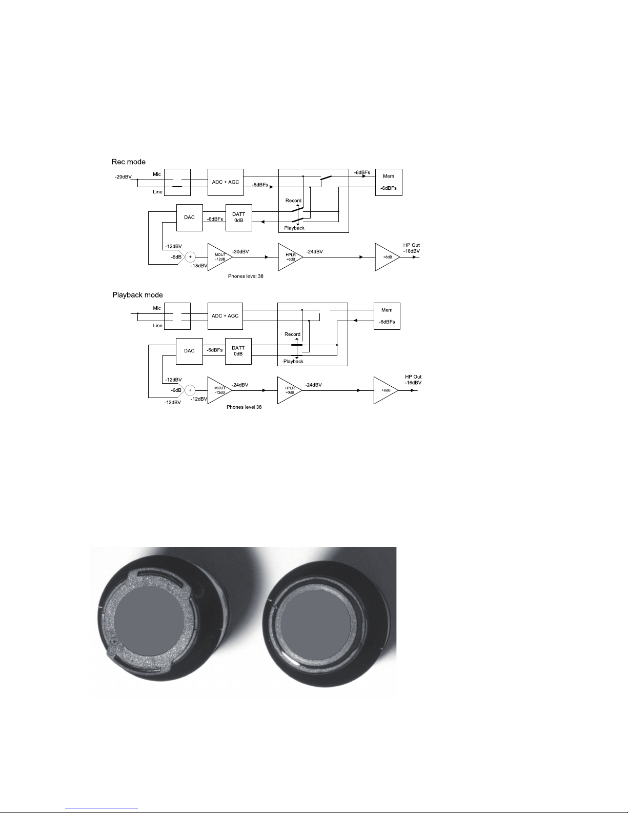
3.3.6 Capsule modules
The module for DRM 85 accommodates an electret capsule of 9.8 mm ∅ with a
bearing ring and a special designed snapped-in filter plate (assembled with silk)
in front of the modul to be optimised to an omnidirectional characteristics. For
DRM 85 C it is an electret capsule of 14.5 mm ∅ with the same filter plate but
different silk on it optimised to a cardioid characteristics. It is easy to distinguish
the cardioid capsule as it has two extensions on either side of the front plate
of the capsule.
Figure 1: Capsule differences
Cardioid Omni-directional
DRM 85-C, DRM 85
12/41 09/2007
-30
-40
-50
-60
dBrA
Hz
DRM 85-C, DRM 85
09/2007 13/41
-10
-20
-30
-40
-50
dBV
Hz
 Loading...