

Page 1
M550/M551 Level 3 Service Manual Page1
MM555500//MM555511 SSEERRVVIICCEE MMAANNUUAALL LLEEVVEELL 33
M550/M551 Doc SP11498 Rev:01 Aug03
©2003 Sendo Ltd. Confidential and Proprietary
Page 2

M550/M551 Level 3 Service Manual Page2
Contents:
Section 1. Introduction
Section 2. Repair Precautions
Sendo guidelines for safe and productive repair work.
Section 3. Product Features and Specifications
General features, technical specifications and warranty details for the
M550.
Section 4. Product Architecture
Functional block diagrams of the RF and logic circuit architecture. Board
layouts are also provided which highlight the main functional areas such as
audio, power supplies and RF circuitry.
Section 5. Product Servicing and Rework Guide
Level 3 repair items, recommended rework equipment and guidelines. Also
included are the assembly-disassembly instructions.
Section 6. Trouble Shooting
Detailed circuit description and repair information to help debug problems
and faults.
Section 7. Software Download
The service centre software download set-up process and its operation.
Section 8. Parts Info
The M550 Parts list including exploded view.
M550/M551 Doc SP11498 Rev:01 Aug03
©2003 Sendo Ltd. Confidential and Proprietary
Page 3

M550/M551 Level 3 Service Manual Page3
Section 1. Introduction
Welcome to the level 3 Service Manual for the Sendo M550/M551. This manual
will guide you to repairing the modules used in the Sendo M550/M551 models.
The M551 is the United States variant – for GSM 850/1900 Mhz.
This manual will help guide you through all repair aspects of the M550/M551 and
provide detailed information on the product.
X102 32 Khz Xtal
M550/M551 Doc SP11498 Rev:01 Aug03
©2003 Sendo Ltd. Confidential and Proprietary
Page 4
M550/M551 Level 3 Service Manual Page4
Section 2
Repair Precautions
M550/M551 Doc SP11498 Rev:01 Aug03
©2003 Sendo Ltd. Confidential and Proprietary
Page 5

M550/M551 Level 3 Service Manual Page5
Important!
Please read the following cautions, notes and warnings
before progressing through this manual or undertaking
any repair action. Remember: SAFETY
FIRST!
AC Main Lead/Power Cord:
Always ensure that ALL AC mains leads used in the repair area are in good condition
and checked regularly. Care must be taken not to damage the lead as this could result
in fire or electric shock.
Battery Pack:
ONLY use original Sendo supplied batteries and chargers with the M550/M551.
DO NOT short the battery terminals together.
Keep the battery pack away from fire and sources of ignition.
Remember to recharge the battery pack after each use.
Before YOU Power up the M550/M551:
• Only switch on the telephone’s power once the test or installation set-up is complete.
• Switching on at the wrong time may result in electric shock or damage to system
components.
• Always ensure that the power is switched off before making connections /
disconnection’s.
• It is important to check that the correct DC voltage is applied to the M550/M551 to
prevent electrical damage.
M550/M551 Doc SP11498 Rev:01 Aug03
©2003 Sendo Ltd. Confidential and Proprietary
Page 6

M550/M551 Level 3 Service Manual Page6
Component Polarity +/-
Always check the polarity of connections and components before soldering.
Particular attention must be paid to I.C’s, diodes, transistors, capacitors and
any other semiconductor device that is polarity dependent.
Electrostatic Damage (ESD):
Semiconductor devices are easily damaged by electrostatic discharge. Many of the
procedures detailed in this manual involve disassembly of the equipment and therefore
handling of the printed circuit boards.
To protect these devices from ESD a wrist strap connected to ground must be worn. In
addition to this the work surface must be covered with an anti-electrostatic mat, which
should also be grounded.
If printed circuit boards are to be stored without being re-assembled into
their equipment, then they must be kept in an anti-electrostatic bag.
Grounding:
Each piece of test equipment should be electrically grounded. A third
(grounding) pin is provided as a safety feature. Ensure that the electrical
outlet also contains this feature.
Cosmetic Protection during Repair Work:
Always ensure that the working surface is kept clean and free from abrasive materials.
The LCD is very susceptible to scratches and damage. It should be
covered with clear adhesive vinyl while the equipment is disassembled.
Storage of Faulty Components:
Any components that are replaced due to failure should be kept safely in an
anti-electrostatic container. Sendo’s Quality or Research & Development
Departments may require them to make quality and reliability investigations.
M550/M551 Doc SP11498 Rev:01 Aug03
©2003 Sendo Ltd. Confidential and Proprietary
Page 7

M550/M551 Level 3 Service Manual Page7
No Fault Found Equipment:
In some cases the reported symptom may not be apparent. You may subject the
equipment to a controlled amount of stress, vibration and temperature variation to see if
the fault occurs.
Care should be taken not to apply excessive stress or vibration or extreme temperature
variations as further faults may develop.
Soldering and Disordering :
Fast, accurate and high quality soldering is required to minimise the risk of heat
damage to the electronic components. ALL rework must follow methods set out in IPC-
7711 (Rewpork of Electrical Assemblies). NO joint should be touched up more than
twice. Wire modifications are not permitted. BGA or fine pitch devices may not be
reflowed more than once.
Short Circuits:
Care must be taken to avoid short circuits. Soldering, solder dust, screws, metal
clippings, metal wrist watches etc. can cause short circuits on PCBs which may result in
component damage.
Test Equipment Calibration:
Your test equipment should be calibrated before use. Frequent calibration is essential
to ensure high quality and reliable repairs.
Cleaning:
Before cleaning ensure that the telephone is switched off and disconnected
from the power source. Cleaning should be done using a soft dry cloth. If
the equipment is heavily soiled a soft cloth soaked in a mild synthetic
detergent diluted in water may be used.
Never use benzene or any other chemicals to clean the equipment.
RF Shielding:
M550/M551 Doc SP11498 Rev:01 Aug03
©2003 Sendo Ltd. Confidential and Proprietary
Page 8

M550/M551 Level 3 Service Manual Page8
It is advisable to carry out detailed measurements and repair (in particular
RX) in a shielded area to minimise RF interference.
AC Adapter and Battery Charger:
The AC adapter and battery chargers are for indoor use only. Ensure that
the devices are not exposed to rain or moisture.
Electrical Safety:
Electrical equipment is hazardous if misused. Any repairs must be carried out with care
and only by authorised personnel.
Ensure all power sources are switched off and power cords removed before
undertaking any repairs.
Hazardous Waste:
The battery pack, if incorrectly disposed of, is an environmental hazard. It must be
disposed of in accordance with the regulations of the country concerned.
Never dispose of the battery pack in fire or water.
Confidentiality:
The circuitry within this equipment contains several components that are
regarded as company confidential. Only use Sendo authorised parts as
replacements.
RF Injury:
To avoid RF injury, direct exposure to radio frequency energy should be
avoided. In particular, exposed parts of your body (especially the eyes and
face) should not come into contact with the antenna while the equipment is
transmitting.
M550/M551 Doc SP11498 Rev:01 Aug03
©2003 Sendo Ltd. Confidential and Proprietary
Page 9

M550/M551 Level 3 Service Manual Page9
Storage Conditions:
It is recommended that the following storage conditions should be avoided to prevent
damage to the equipment: Dusty.
Humid.
Near to magnetic equipment.
In direct sunlight.
Ventilation:
Repair areas should be well ventilated and fume extraction systems should
be installed where necessary. Potential hazardous substances are solder
fumes, flux, alcohol etc.
PCB Handling:
It is recommend that cotton or latex gloves are worn during repair work. This is to
protect your hands from chemical contamination and to protect the PCBs from
fingerprints and humidity.
SIM Card:
• Do not bend.
• Clean by using a soft dry cloth.
• Please note that a modified SIM card will be required to perform conducted rf
measurements via the rf switch. See section 5. Product Servicing and Rework Guide.
M550/M551 Doc SP11498 Rev:01 Aug03
©2003 Sendo Ltd. Confidential and Proprietary
Page 10

M550/M551 Level 3 Service Manual Page10
Section 3
Product Features and
Specifications
M550/M551 Doc SP11498 Rev:01 Aug03
©2003 Sendo Ltd. Confidential and Proprietary
Page 11
M550/M551 Level 3 Service Manual Page11
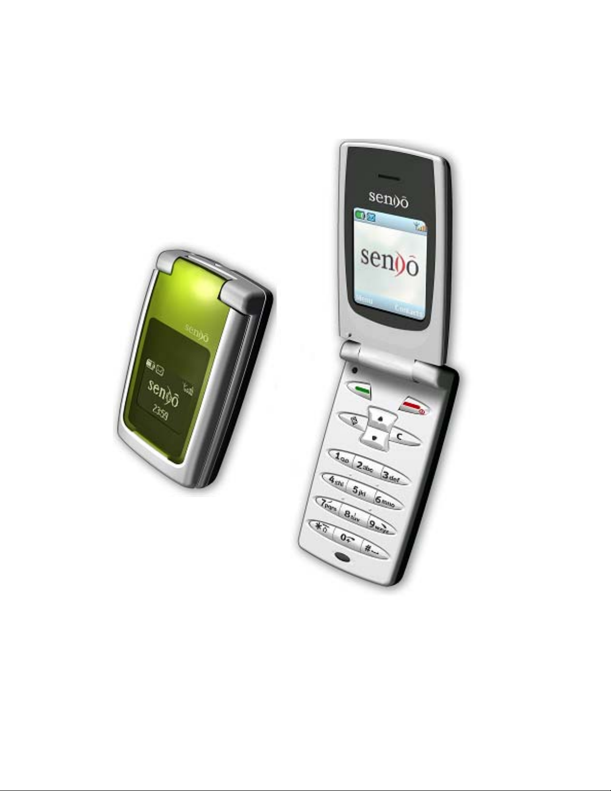
PPrroodduucctt DDeessccrriippttiioonnss
M550 IMEI TAC code: 35188400 (M551:001031A)
Model Type: SND550/SND551
NNeettwwoorrkk SSeerrvviicceess
Dual Band E-GSM 900 / GSM 1800 - M550
Dual Band GSM 850 / GSM 1900 - M551
Automatic switching between bands
Manual and automatic network selection
HR / FR / EFR codec for GSM 900 / 1800
M551 includes AMR FR and AMR HR
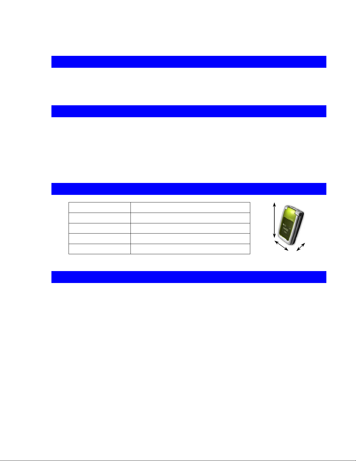
DDiimmeennssiioonnss aanndd WWeeiigghht
Length (a)
Width (b) 19.6mm at widest point
Depth (c) 45mm at thickest point
82mm at longest point
t
a
Weight 77g
Volume 68cc
PPoowweerr MMaannaaggeemmeennt
Talk Time: Up to 180-400 mins*
Standby Time: Up to 120-300 hours*
Game-Play up to 3 hours*
Sim Type:
Charging time: <2 hours
Battery: Li-Ion cell - 650Ah, 3.7vdc
Linear charger (240v Euro plug, 240v UK plug, 220v China plug, 110v US
plug or 220v Australian plug)
* Battery life is Network dependent; variations may occur.
The M550/M551 works closely with the network and the standby and talk
times achieved depend upon this. In particular the location of the HHP
within the network, the type of SIM, reception of area messages, the use of
Micro 3V or 5V SIM
t
c
b
M550/M551 Doc SP11498 Rev:01 Aug03
©2003 Sendo Ltd. Confidential and Proprietary
Page 12

M550/M551 Level 3 Service Manual Page12
Full Rate speech or Enhanced Full rate speech and other factors will affect
both standby and talk times.
MM555500 CCoorree FFeeaattuurrees
s
Product Features
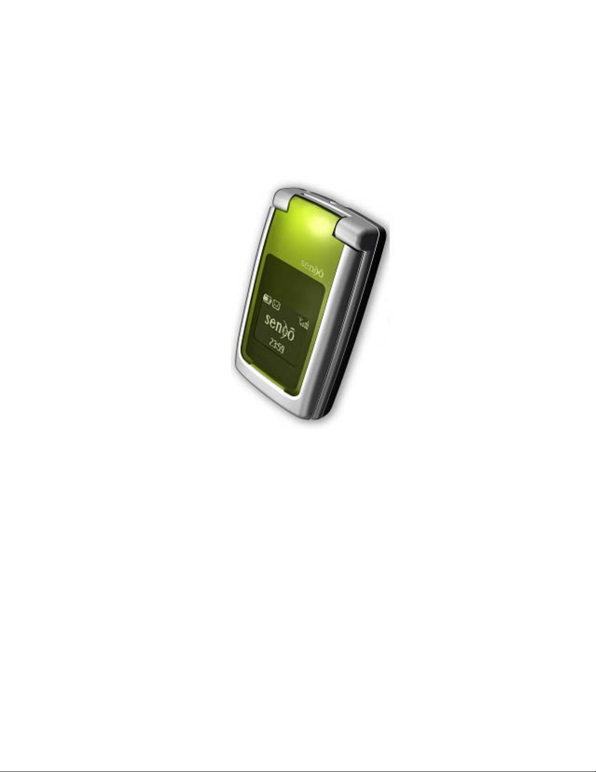
Clamshell design with internal antenna
Size: 77g, weight: 68cc
Dual display, outer: reverse video, 96x64 pixels
Inner colour display – up to 4096 colours
Customizable colour themes
On phone dynamic memory-up to 500 phone book entries
Colour EMS
Wap 1.2.1 colour browser and GPRS class 8
Colour games
Tegic T9 text input, built in SMS chat and SMS templates
Animated graphics and sound
Dual Band (M550:E-GSM 900/1800, M551:GSM850/1900
Stand by time up to 180-400 hours*
Talk time up to 120-300 mins*
Gameplay up to 3 hours*
*talktime and standby times depend upon network conditions and the way you use the phone.
M550/M551 Doc SP11498 Rev:01 Aug03
©2003 Sendo Ltd. Confidential and Proprietary
Page 13

M550/M551 Level 3 Service Manual Page13
WWaarrrraannttyy DDeettaaiills
s
Limited Warranty
Sendo International Limited (“Sendo”) warrants, subject to the exclusions and limitations set forth below, that your
cellular phone, battery and accessories (collectively “Product”) is free from defects in materials and workmanship
according to the following terms and conditions:
1. The limited warranty for the Product commences on the date of purchase and continues for a period of one
(1) year from that date. Upon request from Sendo, you, (the “Consumer”) must prove the date of the original
purchase of the Products by dated itemised receipt.
2. The limited warranty extends to the original purchaser of the Product, the Consumer, and is not assignable
or transferable to any subsequent purchaser or user.
3. The warranty extends only to Consumers who purchase the Product in the market for its intended sale.
4. During the limited warranty period, Sendo will repair, or replace, at Sendo's sole option, any defective parts, or any
parts that will not properly operate for their intended use with new or refurbished replacement items if such repair or
replacement is needed because of a malfunction or failure of the Product during normal usage. No charge will be
made to the Consumer for any such parts. Sendo will also pay for the labour charges incurred by Sendo in repairing
or replacing the defective parts. This warranty does not apply to any damage or failure to operate caused by use of
the Product other than in accordance with the instructions contained in the User Manual, or for periodic maintenance
or repair due to normal wear and tear. Sendo's limit of liability under the limited warranty shall be the actual cash
value of the Product at the time the Consumer returns the Product for repair, determined by the price paid by the
Consumer for the Product less a reasonable amount for usage. Sendo shall not be liable for any other losses or
damages. These remedies are the Consumer's exclusive remedies for breach of warranty
5. The warranty will be invalidated if any of the following circumstances are applicable:
a) The Product has been subject to abnormal use, abnormal conditions, improper storage, exposure to
moisture or dampness, unauthorized modifications, unauthorized connections, unauthorized repair, misuse,
neglect, abuse, accident, alteration, improper installation, or other acts which are not the fault of Sendo,
including damage caused by shipping.
b) Physical damage to the surface of the Product, including scratches or cracks in or to the outside casing or
Liquid Crystal Display, or damages caused by dropping the Product.
c) The Product has been damaged from external causes such as liquid, water, collision with an object, or from
fire, flooding, sand, dirt, windstorm, lightening, earthquake or damage from exposure to weather conditions,
an Act of God, or battery leakage, theft, blown fuse, or improper use of any electrical source, damage
caused by computer or internet viruses, bugs, worms, Trojan Horses, cancelbots or damage caused by the
connection to other products not recommended for interconnection by Sendo.
d) The Product has been altered or repaired by anyone other than an authorised Sendo service centre or if it
has been used with unapproved accessories or other ancillary items.
e) For adaptations or adjustments made to the Product to comply with local standards in any country other than
one for which the Product was designed and manufactured.
f) Loss of integrity of any user data stored in the Product or any storage device used in conjunction with the
Product at any time
g) The Sendo authorised service centre was not advised by the Consumer in writing of the alleged defect or
malfunction of the Product within fourteen (14) days after the expiration of the applicable limited warranty
period.
M550/M551 Doc SP11498 Rev:01 Aug03
©2003 Sendo Ltd. Confidential and Proprietary
Page 14

M550/M551 Level 3 Service Manual Page14
h) The Product serial number plate or the accessory data code has been removed, defaced or altered.
i) The defect or failure to operate was caused by the defective function of the cellular system or by inadequate
signal reception.
6. Any implied warranty of satisfactory quality, merchantability, or fitness for a particular purpose or use, shall be
limited to the duration of the foregoing written warranty. Otherwise, the foregoing warranty is the Consumer’s sole
and exclusive remedy and is in lieu of all other warranties, express or implied. Sendo does not warrant uninterrupted
or error free internet or data connections. Sendo shall not be liable for special, incidental or consequential damages,
including but not limited to, loss of anticipated benefits or profits, loss of savings or revenue, punitive damages, loss of
use of the product or any associated equipment, loss of data, cost of capital, cost of any substitute equipment or
facilities, downtime, the claims of any third parties, including customers, and injury to property, resulting from the
purchase or use of the product or arising from breach of the warranty, breach of contract, negligence, strict tort, or any
other legal or equitable theory, even if Sendo knew of the likelihood of such damages. Sendo shall not be liable for
delay in rendering service under the limited warranty, or loss of use during the period that the product is being
repaired or loss of data.
7. Some jurisdictions do not allow limitation of how long an express or implied warranty lasts and so the one year
warranty period referred to above may not apply, to you, the Consumer. Some jurisdictions do not allow the exclusion
or limitation of incidental and consequential damages and so to the extent that such limitations are not allowed, the
above limitations or exclusions may not apply, to you, the Consumer. This limited warranty gives the Consumer
specific legal rights and the Consumer may also have other legal rights under the legislation of some jurisdictions.
These legal rights vary from jurisdiction to jurisdiction and are not prejudiced by anything contained in this limited
warranty. It also means that in some jurisdictions our responsibility to you the Consumer may be more extensive than
in other jurisdictions.
8. The Consumer shall take the following steps to make a claim under this limited warranty:
a) Please do not ship the Product for service without first contacting the nearest Sendo Authorised Service
Centre.
b) Contact information for the world-wide network of Sendo authorised service centres is available at
www.sendo.com
c) If the Product qualifies for in-warranty service, the Consumer must prove the date of the original purchase of
the Products by a dated proof of purchase.
d) Back up all data. If the Consumer has sensitive information stored on the Product copy it to another device
and delete it from the Product before repair.
e) The Consumer must ship the Product prepaid and insured. Expenses related to removing the Product from
an installation are not covered under this limited warranty.
f) If the Product is returned for service and the Product is deemed out of warranty under the terms and
conditions of this warranty, the Consumer will be notified and given an estimate of the applicable charges. If
the estimate is refused a minimum service fee for collection, inspection and quotation of said product would
be due.
9. Subject to any more extensive legal rights granted to the Consumer by law of the Consumer’s jurisdiction, Sendo
neither assumes nor authorizes any authorised service centre or any other person or entity to assume for it any other
obligation or liability beyond that which is expressly provided for in this limited warranty including the provider or seller
of any extended warranty or service agreement.
10. This is the entire warranty between Sendo and the Consumer, and supersedes all prior and contemporaneous
agreements or understandings, oral or written, and all communications relating to the Product, and no representation,
promise or condition not contained herein shall modify these terms.
11. This limited warranty allocates the risk of failure of the Product between the Consumer and Sendo. The allocation
is recognized by the Consumer and is reflected in the purchase price of the Product.
12. Diagnostic instructions and other service information is available free of charge at www.sendo.com
out of warranty repair costs and charges is available at www.sendo.com
. Information on
.
M550/M551 Doc SP11498 Rev:01 Aug03
©2003 Sendo Ltd. Confidential and Proprietary
Page 15
M550/M551 Level 3 Service Manual Page15
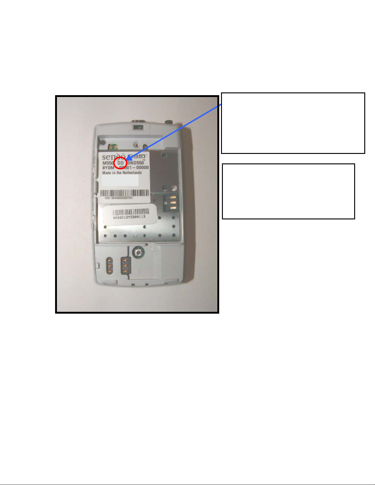
Warranty Details
Identifying the manufacturing date on a unit.
EXAMPLE,
First LETTER = YEAR
Second LETTER = MONTH
DD = 2003, April
NOTE:
THE CODES HAVE ONLY BEEN
ISSUED ON MANUFACTURED
UNITS AFTER SEPTEMBER 2001.
M550/M551 Doc SP11498 Rev:01 Aug03
©2003 Sendo Ltd. Confidential and Proprietary
Page 16

M550/M551 Level 3 Service Manual Page16
The Table below shows the manufacturing dates and their codes.
WWaarrrraannttyy TTaabbllee
CODE MANUFACTURED DATE OUT OF WARRENTY END OF
BI
BJ
BK
BL
CA
CB
CC
CD
CE
CF
CG
CH
CI
CJ
CK
CL
DA
DB
DC
DD
DE
DF
DG
DH
DI
DJ
DK
DL
EA
EB
EC
ED
EE
EF
SEPT 2001 NOV 2002
OCT 2001 DEC 2002
NOV 2001 JAN 2003
DEC 2001 FEB 2003
JAN 2002 MAR 2003
FEB 2002 APR 2003
MAR 2002 MAY 2003
APR 2002 JUNE 2003
MAY 2002 JULY 2003
JUNE 2002 AUG 2003
JULY 2002 SEPT 2003
AUG 2002 OCT 2003
SEPT 2002 NOV 2003
OCT 2002 DEC 2003
NOV 2002 JAN 2004
DEC 2002 FEB 2004
JAN 2003 MAR 2004
FEB 2003 APR 2004
MAR 2003 MAY 2004
APR 2003 JUNE 2004
MAY 2003 JULY 2004
JUNE 2003 AUG 2004
JULY 2003 SEPT 2004
AUG 2003 OCT 2004
SEPT 2003 NOV 2004
OCT 2003 DEC 2004
NOV 2003 JAN 2005
DEC 2003 FEB 2005
JAN 2004 MAR 2005
FEB 2004 APR 2005
MAR 2004 MAY 2005
APR 2004 JUNE 2005
MAY 2004 JULY 2005
JUNE 2004 AUG 2005
M550/M551 Doc SP11498 Rev:01 Aug03
©2003 Sendo Ltd. Confidential and Proprietary
Page 17
M550/M551 Level 3 Service Manual Page17
Section 4
Product Architecture
M550/M551 Doc SP11498 Rev:01 Aug03
©2003 Sendo Ltd. Confidential and Proprietary
Page 18
M550/M551 Level 3 Service Manual Page18
r
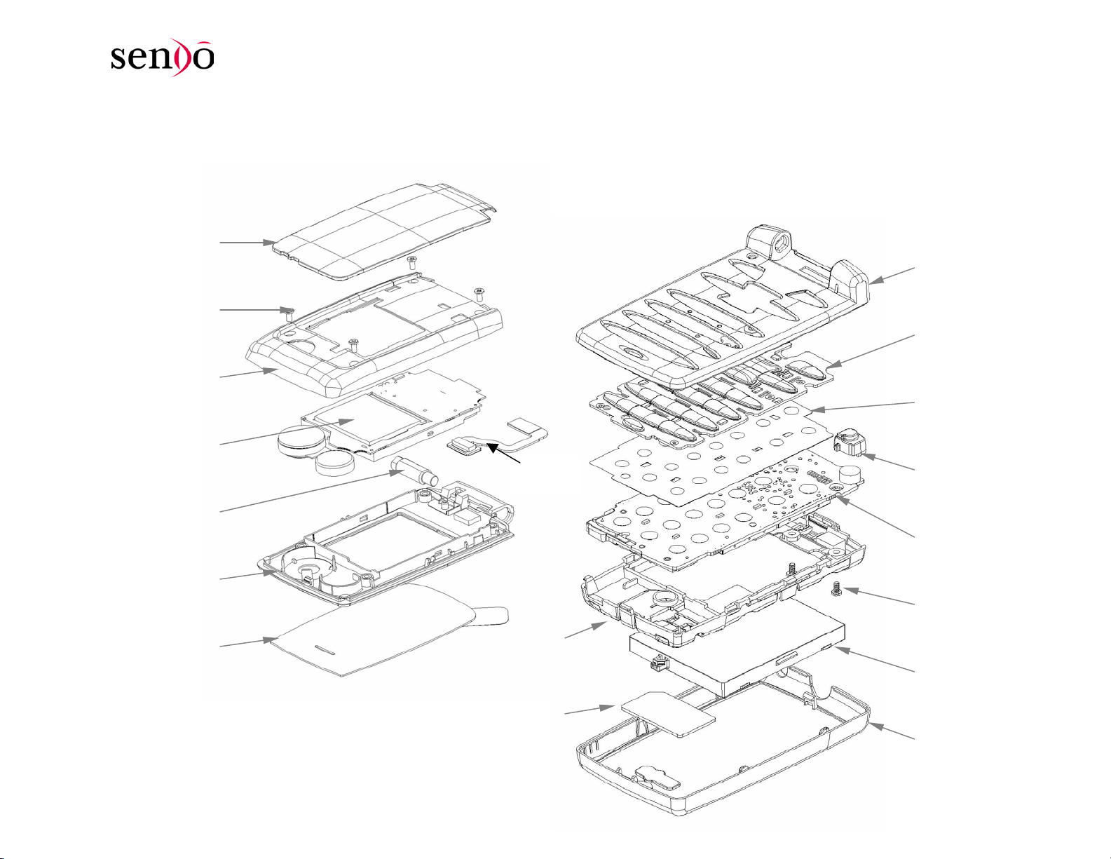
Section.1: M550 Product Structure – Exploded view
Outer Lens Assy
Screw (4pc)
Outer Ring Assy
LCD Module
FPC
Front Hsg Assy
Keypad
Metal-dome
Mic Gasket
Inner Hsg Assy
Lens Assy
M550/M551 Doc SP11498 Rev:01 Aug03
©2003 Sendo Ltd. Confidential and Proprietary
Hinge
Battery
Holde
SIM
PCBA
Screw (2pc)
Battery
Battery Cover
Page 19
M550/M551 Level 3 Service Manual Page19
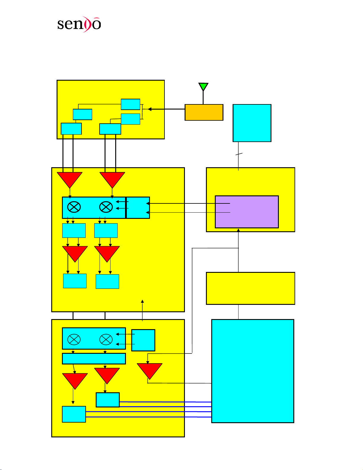
Logic circuit Architecture
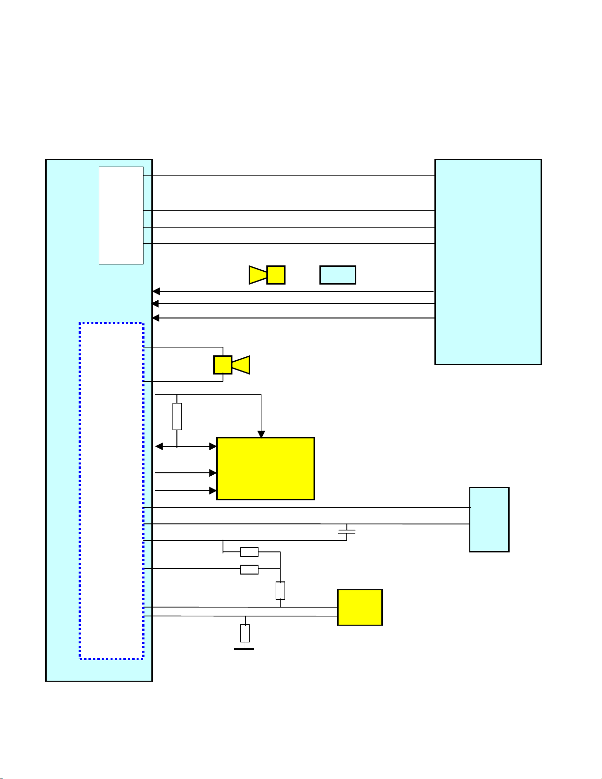
Part a: Audio Circuits and SIM Interface
IOTA
IC200
VOICE
BAND
SERIAL
PORT
K3
G5
H5
F5
VOIC
BAND
CODER/
DECODER
J9
J10
E
SIM_IO
SIM_CLK
SIM_RST
K9
C7
G7
J8
J7
H7
BB_VCLK
BB_VFS
BB_VDX
BB_VDR
(Buzzer)
BB_EARP
BB_EARN
(Ear Piece)
SIM_VCC
IO VDD
CLK
RST
BB_MIC_REF_P
BB_MICP
BB_MICN
BUZZ_EN
T401
BB_SIM_IO
BB_SIM_CLK
BB_SIM_RST
SIM Reader (X402)
BB_AUX_MIC
MIC
N12
M13
N13
P14
CALYPSO
K7
IC100
X200
(Audio Jack)
AUXOP
3
2
Part b:
M550/M551 Doc SP11498 Rev:01 Aug03
©2003 Sendo Ltd. Confidential and Proprietary
Page 20
M550/M551 Level 3 Service Manual Page20
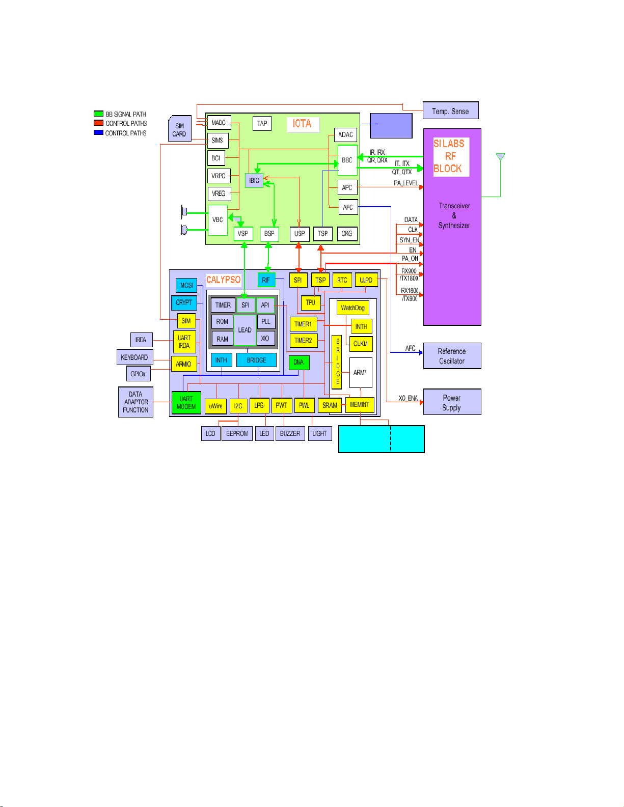
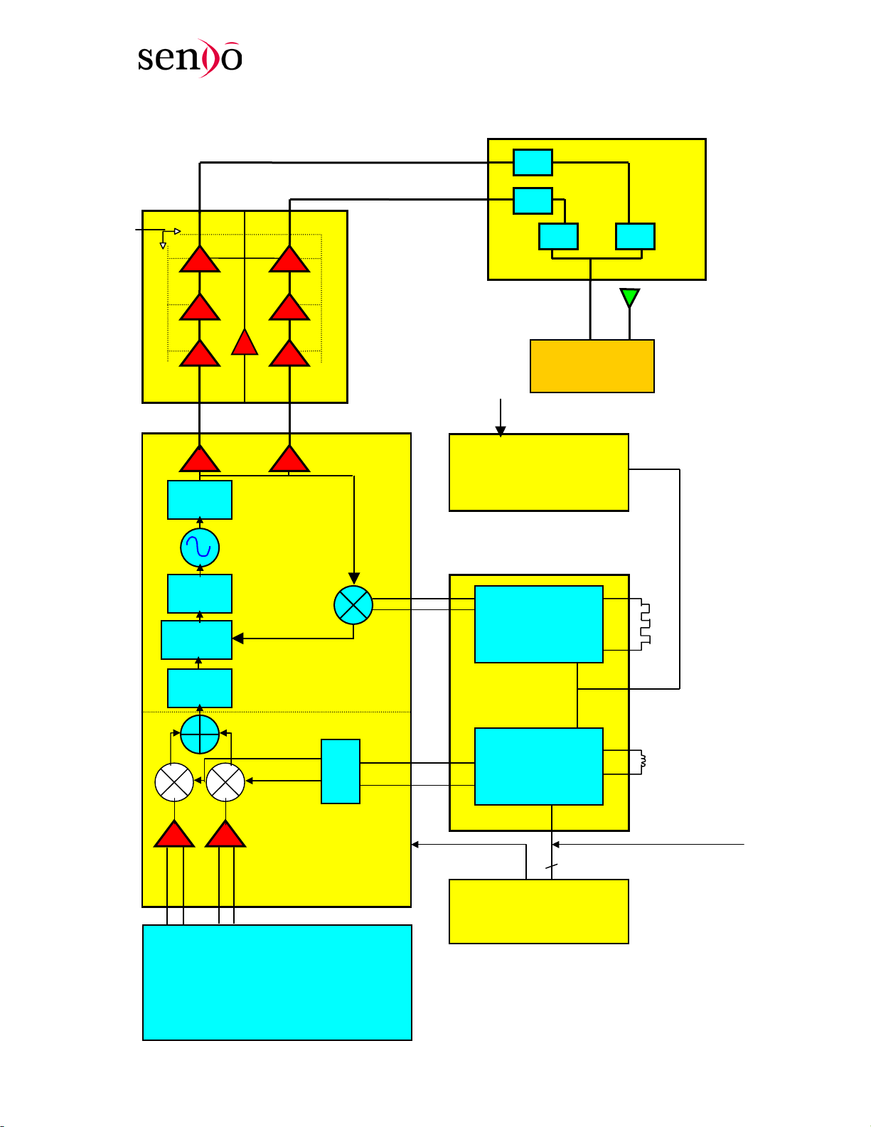
Part b: Logic Circuit Block Diagram
CHGR
IC200
IC100
(X102 – 32Khz)
The main functional blocks of Calypso (IC100) are:
• ARM Megamodule (ARM7TDMIE)
• DSP Megamodule (S28C128)
• Memory Interface & Memory Protection Unit
• Interrupt Handler (INTH)
• Clock Management (CLKM)
• Timers
• General Purpose IO (ARMIO)
• UART – IRDA and UART – MODEM
• UWire Interface (UWIRE)
• I2C Master Serial Interface (I2C)
• Serial Port Interface (SPI)
• Pulse Width Tones (PWT)
• Pulse Width Light (PWL)
• Light Pulse Generator (LPG)
• Debug Unit (DU)
The main functional blocks of IOTA (IC200) are:
• Automatic Frequency Control Unit
• Auxiliary Drivers
• Automatic Power Control Unit
• Baseband Codec
• Back up Battery Switch, Battery Charger Control
• Baseband Up / Down Link, Baseband Serial Port
• Clock Generator
• LDO Voltage Regulators, Voltage Reference, Power Control
• Monitoring Analogue to Digital Converter
• SIM interface
• Time Serial Port, Test Access Port
• Microcontroller Serial Port
• Voice band Codec
• Voice Serial Port
Flash
SRAM
IC300
M550/M551 Doc SP11498 Rev:01 Aug03
©2003 Sendo Ltd. Confidential and Proprietary
Page 21
M550/M551 Level 3 Service Manual Page21
A
Section.2: Radio Architecture
Part a: Receiver Block Diagram
IC500 RF Switch
SW
saw
6 7 9 10
PCS GSM
20 19 22 21
saw
LPF
LPF
ADC
ADC
1 2
ION IOP
12 11
Channel filter
DAC
DAC
IC600
Doc M550/M551 Revision June 2
©2003 Sendo Ltd. Confidential and Proprietary
Demodulator
HPF
LPF
Π/2
IC601
IF Mixer
IOP
ION
CLKP
CLKN
100
KHz
NT
13 RF_LON 23
12 RF_LOP 24
7
RF_CLK_13M
4
5
2
3
D9
D10
C9
C10
003
IC100
CALYPSO
PDNB
RF_TPU_DATA_OUT (SDO)
3
RF_TPU_DATA IN (SDI)
IC602
Synthesiser
RF PLL
7
3
IICC660033
((1133MMhhzz))
RF_AFC
IICC220000
IOTA
RF_IP
RF_IN
RX = I+Q
RF_QP
RF_QN
Page 22
M550/M551 Level 3 Service Manual Page22
)
part b: Transmitter Block Diagram
RF_PA_CTL_EN
3
QP QN IP IN
VCCOUT
9 10 11
7 6 1
VRAMP
÷1 DCS
÷2 GSM
(IC200)
TX_VCO_GSM TX_V CO_PCS
IC700
25 24
IC601
LPF
∅detector
LPF
OFFSET PLL
÷
TX = I+Q
IICC220000 ((IIOOTTAA))
©2003 Sendo Ltd. Confidential and Proprietary
EGSM_PA_TX
PCS_PA_TX
Power Amps
(PA
13 RF_LON 24
14 RF_LOP 23
10 IF_ LON 27
11 IF_ LOP 28
IOP
ION
CLKP
CLKN
M550/M551 Doc SP11498 Rev:01 Aug03
1
11
IC500 RF Switch
LPF
LPF
HPF LP F
ANT
RF_AFC (IC200)
MF501
IICC660033
13Mhz Reference
RF PLL
IC602
IF PLL
3
IICC660000
9
2
V
CXO_13MHZ
3
7
PDNB
RF_TPU_DATA_OUT (SDO)
RF_TPU_DATA IN (SDI)
Page 23
M550/M551 Level 3 Service Manual Page23
)
Section.3: M550 Functional Areas
Part a: Keypad, MIC and Backlight Area’s
In this section are shown the locations of the main keypad, backlight and Mic locations.
Side.1
X404: MIC
Keypad Area (Shown without Metaldome sheet fitted
MF_110: Flip detect contact pad
M550/M551 Doc SP11498 Rev:01 Aug03
©2003 Sendo Ltd. Confidential and Proprietary
Backlight LED’s (D402-D410)
Page 24
M550/M551 Level 3 Service Manual Page24
p
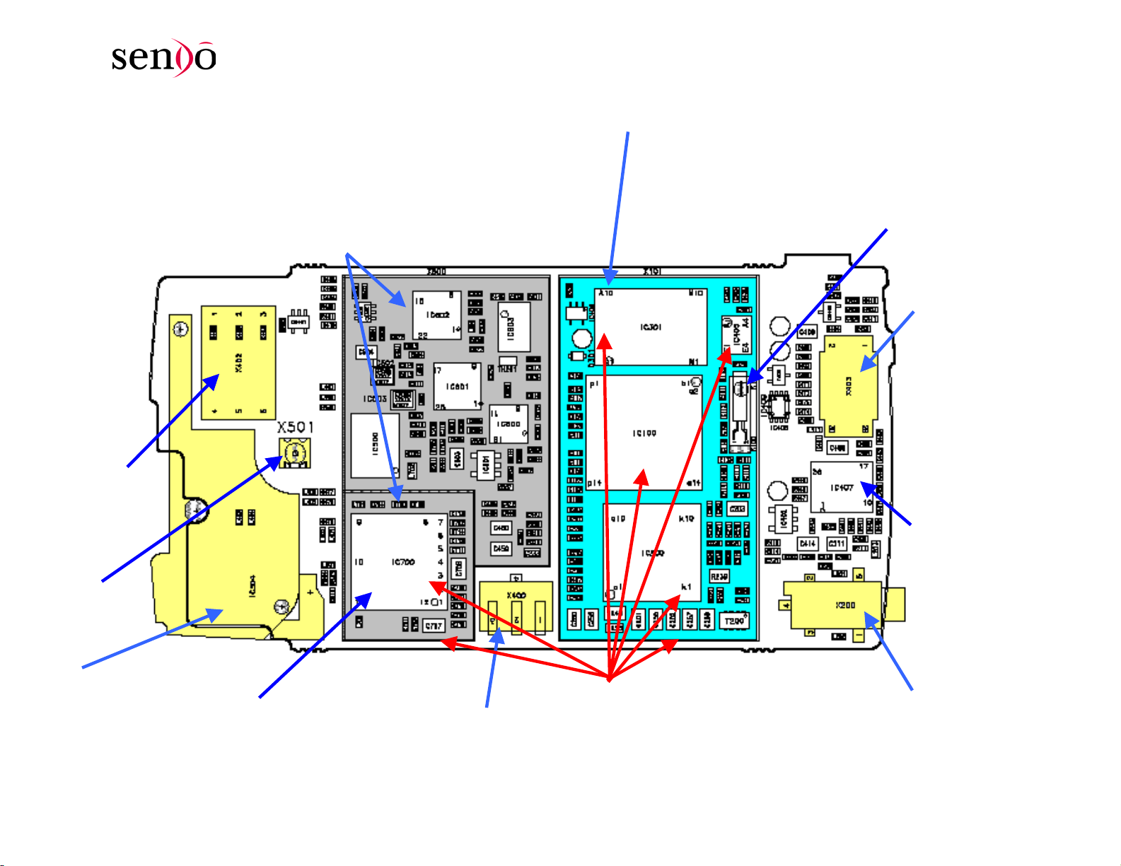
Section.3: Functional Areas – Cont’d
Part b: RF and Logic functional blocks
Here are shown the main functional parts of the logic and RF circuits.
Baseband Circuitry area (in blue)
Side.2
X402 - SIM Interface
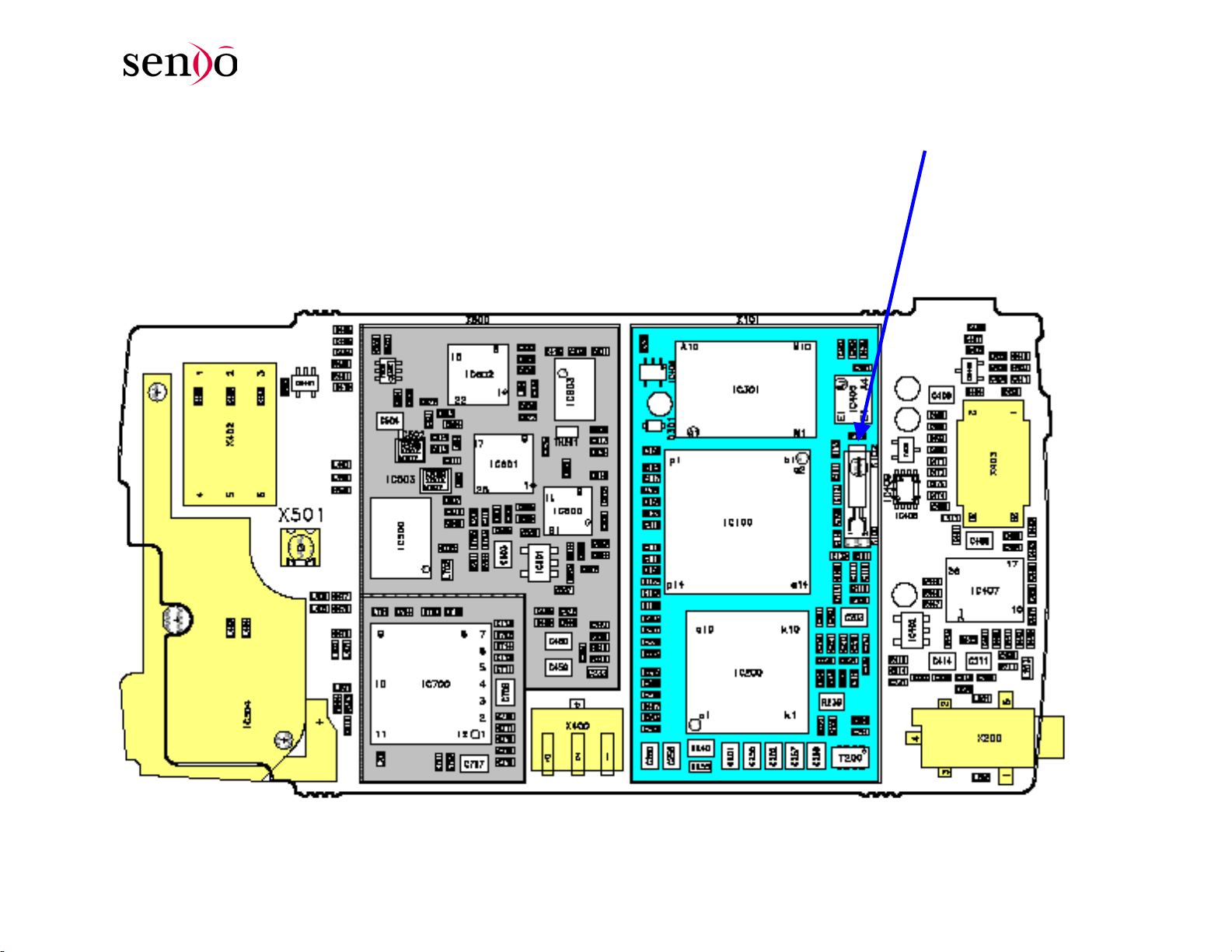
X501 – Antenna
RF Switch
RF Circuitry areas (in grey)
X403 Connector
(Connects PCB to
LCD Module via
*FPC).
IC407 Sound Synthesiser
PA
IC504 - Antenna
IC700 – TX Power Amplifier
and associated circuit.
M550/M551 Doc SP11498 Rev:01 Aug03
©2003 Sendo Ltd. Confidential and Proprietary
X400 - Battery Connector
and DC
ower supply
Non-replaceable Parts
IC100 “Calypso” (BGA-Underfilled)
IC200 “IOTA (BGA –Underfilled)
IC301 Flash/SRAM – Underfilled)
IC405 LCD Driver
IC700 Power Amplifier
Shielding Frames (BB & RF)
X200 - Audio Jack and
charging socket.
Page 25
M550/M551 Level 3 Service Manual Page25
IC603 13Mhz Clock
Main RF Circuit devices:
IC500: TX/RX path switching IC
IC501: RF 2.8V POWER SUPPLY (VCC_2V8_RF)
IC600: RX Demodulator
IC601: IF+RF Modulator and Mixer
IC602: IF+RF Synthesisor (PLL- Phase Locked Loop)
X501: Mechanical rf switch
IC603:13Mhz Clock
IC502: GSM1800 Rx band pass filter
IC503: GSM900 Rx band pass filter
IC504: Antenna
X102 32 Khz Xtal
M550/M551 Doc SP11498 Rev:01 Aug03
©2003 Sendo Ltd. Confidential and Proprietary
Page 26

Page:26
M550/M551 Level 3 Service Manual
Section 5
Product Servicing
M550/M551 Doc SP11498 Rev:01 Aug03
©2003 Sendo Ltd. Confidential and Proprietary
Page 27

Page:27
M550/M551 Level 3 Service Manual
5.1 Level 1-2 Repair Items
Administration Checks
- Warranty Check
- Phone and Accessories
- DOA Filter Analysis (if required)
- Checking Fault report from customer
Level 1
- NFF
- SWAP
- Outer Bezel
- Inner Bezel
- Battery Cover
- Charger
- Battery
- Accessories
Level 2
- Labels
- Software Upgrade/Blocked Units
- Battery Holder
- Inner Housing
- Outer Ring
- Front Housing
- Keypad
- Board to Board FPC (Flexible Plastic Connector)
- Shielding can covers (Baseband+RF)
- Hinge assembly
- Metaldome
- Mic Gasket
- LCD Module (Replacement only)
- PCB cleaning
- Discreet components which just require soldering to replace
o Charger Socket
o Sim Connector
o Battery Connector
o Mic
o Buzzer, Vibrator and Earpiece (Speaker)
o Backlight LED’s
o Antenna
Level 3
- Components that need replacing after test equipment de-bug analysis
- Internal DAC level calibration, setting internally in phone
- Re-programming IMEI – Security
NOTE : Level 3 repair is restricted on the SND550 as some IC’s are under filled.
M550/M551 Doc SP11498 Rev:01 Aug03
©2003 Sendo Ltd. Confidential and Proprietary
Page 28
Page:28
M550/M551 Level 3 Service Manual
5.2 General Quality Guidelines for Rework
The following guidelines should be followed when either reworking joints or replacing
electronic parts.
• All rework must follow the methods described in part 5.3b – “Prefered rework
methods” and to standard IPC-7711 (Rework of Electric/Electronic Assemblies).
• No joint may be touched-up more than twice.
• Wire modifications are not permitted.
• Any BGA devices on M550, which are underfilled must not be reworked or
replaced.
5.3a Recommended Equipment for Repair
Rework Tools
Soldering Iron: - Lockable temperature-regulated soldering iron station.
E.g. JBC AM6000, Weller WSD80 or Metcal MX-500
Hand Tweezers: - ESD safe flat rounded point
Solder Braid: - Multicore AA or Chemtronics 60-2-10 (size #2)
Solder: - Tin/Copper Lead Free (0.5 – 1.0mm diameter)
Flux: - Cobar 390RX
Flux Applicator: - Boncote BON-102
Torque Driver:- Calibrated to 10Ncm (+/- 1cNm) with bit Posidrive size “0”
Protective Gloves:- Disposable Latex gloves / Finger Cots.
Cover opening Tool* - Available from Sendo.
M550/M551 Doc SP11498 Rev:01 Aug03
©2003 Sendo Ltd. Confidential and Proprietary
Cover Opening tool
Page 29
Page:29
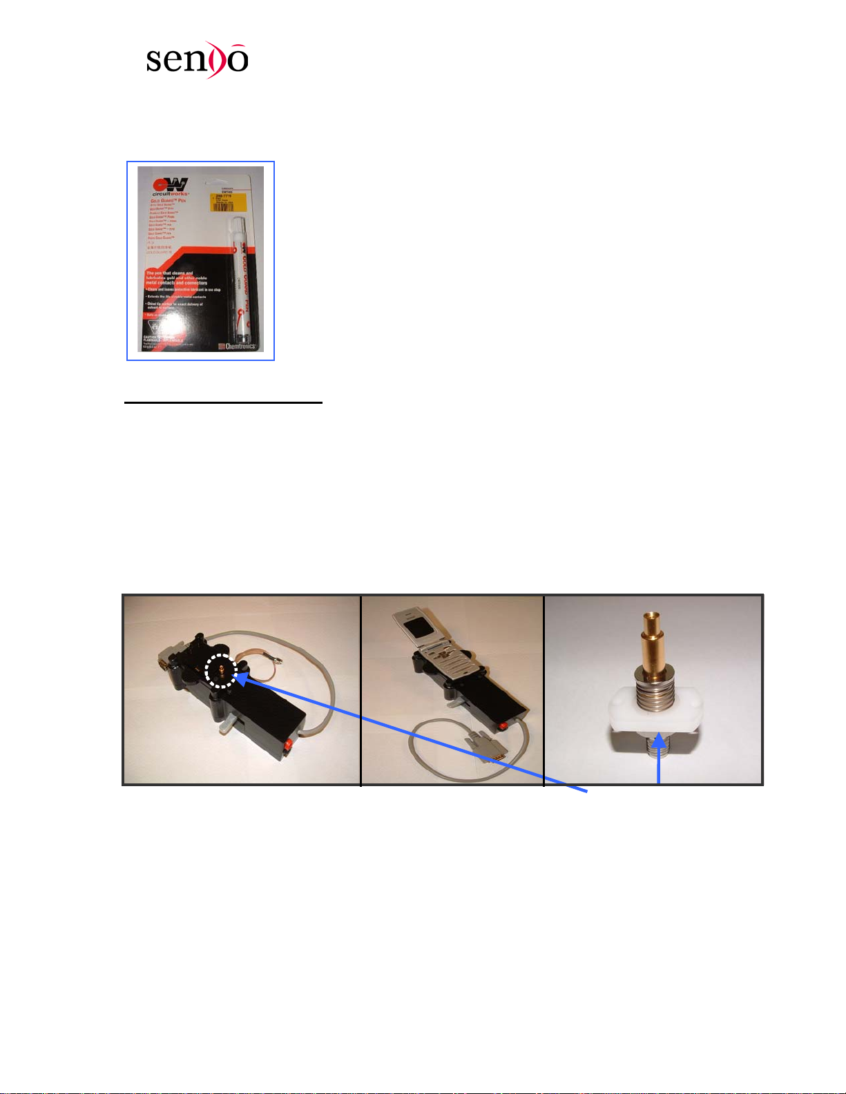
Adaptor fitted to battery eliminator.
RF Note: Can only be used with
battery eliminator.
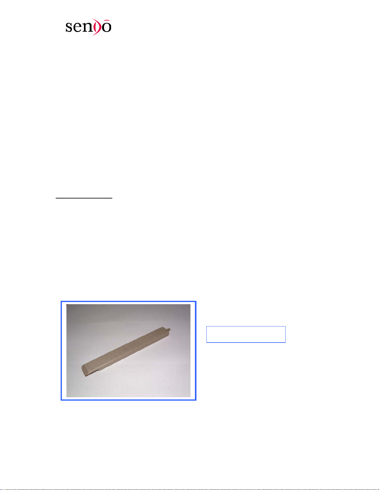
Gold Guard Pen:- (for cleaning all contact pads) as below:-
M550/M551 Level 3 Service Manual
This item is available from: RS Components
Ltd (Part no: 298-7779), Website:rswww.com
Electronic Equipment
Digital Multimeter (DMM)
5V DC Power Supply
GSM Test Set
PC with Windows XP or 2000
Battery Eliminator* :- For software downloading and powering unit. Can also be used
to perform RF measurements**.
**RF adaptor (optional) must also be fitted to
perform measurements).
* Please contact Sendo for Details of aquiring these items
M550/M551 Doc SP11498 Rev:01 Aug03
©2003 Sendo Ltd. Confidential and Proprietary
Page 30
Page:30
M550/M551 Level 3 Service Manual
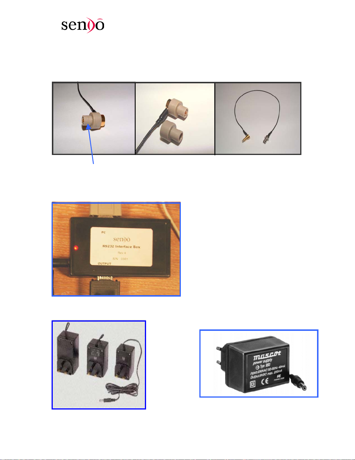
Leaded RF adaptor fitted with support collar*:- for performing RF measurements of
M550/M551 if using standard battery. Plugs directly into rear of M550/M551.
Collar fitted to RF adaptor
Leaded RF adaptor “without" Collar
RS232 Interface Box with 9 VDC power supply and serial cable*
Regulated 9vdc Power Supply for RS232 interface box.
Used to provide DC power to the RS232 Interface Box.
M550/M551 Doc SP11498 Rev:01 Aug03
©2003 Sendo Ltd. Confidential and Proprietary
UK Type
EU Type
Page 31

Page:31
DC Jack/bannana Leads * For power connection from 5V DC power supply to
battery eliminator.
GSM Test SIM :- To perform RF tests on the unit a modified test SIM must be used. A
portion of the test SIM needs to be removed as per the diagram below:-
This enables the RF adaptor(s) access to the RF switch (X501) on the rear of the unit.
* Please contact Sendo for Details of aquiring these items
This portion is removed
M550/M551 Level 3 Service Manual
M550/551 Handling Precautions
Whenever the M5** is either disassembled or assembled extreme care
must be taken in handling any of its parts. Special attention must be paid
when handling the colour LCD module, which can easily be scratched or
damaged. Soft cotton gloves should be worn AT ALL TIMES when
handling any of the M5XXs parts.
For your own safety and to protect the product from damage please
observe the guidelines listed in Section 1: Repair Precautions.
M550/M551 Doc SP11498 Rev:01 Aug03
©2003 Sendo Ltd. Confidential and Proprietary
Page 32

Page:32
M550/M551 Level 3 Service Manual
5.3b Preferred Rework Methods
Part to be Replaced: Microphone (Through-hole device)
Removal
Replacement
Insert legs of mic through holes in pcb and position as in above
picture. Apply iron tip to both leg and pad and apply solder to leg.
keep tip in Place for 3-5 secs to ensure solder melted evenly. Remove
tip and allow to cool, then inspect and clean.
Removal Method
Microphone
For standard through-hole devices, remove any adjacent parts
that are heat sensitive i.e. key pad assembly etc. Set station
temperature to approx 350 degrees and select a suitable hand
piece. Add flux to the solder joints with brush applicator. Tin the tip
with solder and lower over the solder connection. Ensure complete
solder melt and apply the vacuum whilst using a rotating motion of
the hand piece. Keep the hand piece on the pad for no longer than
5 secs at any one time. Remove the mic from the joint, leaving the
vacuum on for a further 3 seconds to clear molten solder from the
head. Repeat for both mic pins and carefully remove device.
Using fluxed solder braid and standard soldering iron, clean
excess solder off pad. If no vacuum system is available then
alternatively use a soldering iron.
Recommended Equipment
Continuous Vacuum De-soldering System
Soldering Iron
Solder Braid
Flux
Flux-Cored Solder
(Alternative approach is 2 irons or hot tweezers for devices not
suitable for a de-solder system)
M550/M551 Doc SP11498 Rev:01 Aug03
©2003 Sendo Ltd. Confidential and Proprietary
Page 33

Page:33
Part to be Replaced: Battery, SIM Connectors and Three Pole Audio Jack
M550/M551 Level 3 Service Manual
Three pole audio Jack
Battery Connector
SIM Connector
Removal Method
Set the heater temperature to approx 425
the device in question. Add flux to the solder joints with Boncote brush
applicator and position the air tip approx 0.5cm away from the component.
Direct the hot air over the component until complete solder melt is achieved
(air guides can be used where appropriate). Grasp the component with
tweezers and remove from the PCB.
Using a fluxed solder braid and standard soldering iron, clean excess solder
off pad.
Note: If replacing the SIM connector using an hot air pencil, the antenna
must first be removed. This is to prevent the hot air from damaging the
plastic antenna body.
Recommended Equipment
Hot Air Pencil with suitable tip.
Soldering Iron
Solder Braid
Flux
Tweezers
Flux-Cored Solder
degrees and install a suitable tip for
Replacement
Set iron temperature to 350 degrees +/- 5% and ensure the iron has been on for the manufacturers recommended warm up period.
Thermal shock the tip on a moist sponge and re-tin the tip. Position the component accurately to the PCB. Apply flux and tack
solder two adjacent corner leads. Apply flux to the remaining leads and individually hand solder each lead in turn. Clean contacts
and solder area if required. Note: Care must be taken not to damage the plastic parts of the connectors or ANY parts
located near the item being replaced.
M550/M551 Doc SP11498 Rev:01 Aug03
©2003 Sendo Ltd. Confidential and Proprietary
Page 34

Page:34
r
Outer Lens
Screw
(4pc)
Outer Ring
LCD
Hinge
Inner Hsg
Lens
M550/M551 Level 3 Service Manual
5.4 Mechanical Assembly Parts
RF
Adaptor
fitted to
battery
Battery
Holde
FPC
SIM
Front Hsg
Keypad
Metal-dome
Mic Gasket
PCBA
Screw (2pc)
Battery
Battery
Cover
Part Descrtion:
1. Inner Hsg Assy:
2. Populated PCBA: Not supplied as a spare part
3. Hinge
4. Screws
5. Mic Gasket
6. LCD Assy
7. Keypad Assy
8. Metal Dome:
9. Front Housing
10. Battery Holder
11. Outer Ring
12. FPC: BOARD TO BOARD FPC
13. Lens
14. Battery Cover
15. Outer Lens
M550/M551 Doc SP11498 Rev:01 Aug03
©2003 Sendo Ltd. Confidential and Proprietary
Page 35

Page:35
M550/M551 Level 3 Service Manual
5.5 Dis-Assembly Procedure
5.5a Battery Holder Cover Removal
Note: Before the M550/M551 can be dis-assembled, the battery and battery cover
must firstly be removed.
BU: Bottom Unit
M550/M551 Doc SP11498 Rev:01 Aug03
©2003 Sendo Ltd. Confidential and Proprietary
Note:
When dis-assembling the product great care must be
taken while opening the covers, as they can easily be
damaged if not handled correctly. Always ensure the
fixing locks/hooking features are released correctly.
Insert the separator tool between BU
front and the Battery holder plastics to
pry open the lower end of the assy both
left and right hand sides.
Remove two screws
securing the Battery
Holder.
Page 36

Page:36
M550/M551 Level 3 Service Manual
5.5a Battery Holder Cover Removal
Continue to pry the left and right
sides to working the tool further
along the housing edge to release all
the side locks.
Note:
To minimise damage to battery
holder and front housing care must
be taken not to damage the side
locks/hooking features on the battery
holder.
With the side locks released, the
battery holder will hinge off the BU
front housing.
M550/M551 Doc SP11498 Rev:01 Aug03
©2003 Sendo Ltd. Confidential and Proprietary
Page 37

Page:37
M550/M551 Level 3 Service Manual
5.5b PCB Removal
Keypad
Disconnect the FPC from the
connector on the pcb. Always remove
the FPC gently as the connector may
be damaged if not handled correctly.
Now the main PCB can be removed
from the front housing. The rubber
keypad can also be removed from the
front housing if required.
ALWAYS ENSURE THAT THE FPC
IS HANDLED CORRECLTY AND IS
NEVER CREASED AS THIS CAN
CAUSE DAMAGE TO ITS
INTERNAL LAYERS.
IMPORTANT NOTICE
Now the Mic gasket can be
removed using tweezers.
M550/M551 Doc SP11498 Rev:01 Aug03
©2003 Sendo Ltd. Confidential and Proprietary
Page 38

Page:38
p
M550/M551 Level 3 Service Manual
5.5c Dis-assembling the top unit from the front housing
The top unit (TU) can be disconnected from the front housing as shown below.
90 deg
TU (Top Unit)
TU angled @ 90 deg relative to Front cover
Angle the unit as shown so the TU and front
housing are at an angle of 90 deg. This is
because the hinge assembly can only be disassembled/assembled when in this
IMPORTANT NOTICE
osition.
Push centre of hinge body
in arrow direction shown in
RED.
Hinge body
Spring ground
contact “In Position”
Position screwdriver head here.
To separate the TU from the front housing, the hinge body must be pushed backwards
through the locating hole in the front housing. Using a small flat blade screwdriver
(size:3mm), position it as shown above. The head of the screwdriver should be positioned
between the sprung contact and the centre of the hinge body. Care must be taken not to
damage the spring contact when pushing the hinge body backwards through the
locating hole. When the hinge has been pushed through the locating hole the TU and front
housing can then be separated. While separating the TU and front housing, they must be
kept at 90deg as shown above.
M550/M551 Doc SP11498 Rev:01 Aug03
©2003 Sendo Ltd. Confidential and Proprietary
Page 39

Page:39
M550/M551 Level 3 Service Manual
Separating the TU and front housing units.
IMPORTANT: Take care when easing the
FPC through the locating slot in front
housing.
Front Housing
Locating slot
5.5d Dis-assembling the top unit 5.5d Dis-assembling the top unit
Using the opening tool as shown
above carefully remove the outer lens.
This will then give access to the four
screws on the outer bezel.
Note: A new outer lens will have to
be fitted when assembling the unit.
TU
Remove the four fixing screws.
M550/M551 Doc SP11498 Rev:01 Aug03
©2003 Sendo Ltd. Confidential and Proprietary
Page 40

Page:40
M550/M551 Level 3 Service Manual
5.5d Dis-assembling the top unit
Carefully insert the opening tool
between the outer ring and inner
housing as shown above. Slide the
tool down the length of the joint on
both sides and gently ease the
parts apart.
Before fully separating the outer bezel from the
inner housing carefully slide the bezel in the
direction shown. This is so to release the hook
features located on the inner housing from the
bezel.
IMPORTANT: Take care when dis-assembling
the bezel and housing as they can be
damaged if not opened in the correct way.
5.5e Removing the LCD assembly from the inner housing
LCD Assy
Disconnecting the FPC
Using the opening tool gently insert
the one end between the LCD assy
and FPC connector as shown. Then
prise the connector away from the
LCD assy to disconnect it.
Disconnecting the FPC
Now the FPC can be removed via the slot
in the inner housing.
IMPORTANT: Take care not to snag the
FPC or its connector on the inner
housing when removing it.
M550/M551 Doc SP11498 Rev:01 Aug03
©2003 Sendo Ltd. Confidential and Proprietary
Page 41

Page:41
y
A
r
Disconnecting Vibrator, Earpiece+ Polyphonic speaker assembly
Again using the opening tool gently insert the one end between the base
of the vibrator body and inner housing as shown. Then gently prise the
vibrator away from the housing to remove it. The same method can be
used to remove the earpiece/speaker unit. Once these parts have been
disconnected from the inner housing the LCD module can then be
removed. IMPORTANT: Always use gloves when handling the LCD
module as both LCD screens can be easil
5.5f
Replacing the vibrator and earpiece + polyphonic speaker assembly
dhesive backing tape*
E/P+P-Spkr
Remove resin encapsulate
M550/M551 Doc SP11498 Rev:01 Aug03
©2003 Sendo Ltd. Confidential and Proprietary
Vibrator
M550/M551 Level 3 Service Manual
Earpiece+P-Speaker
scratched/damaged.
Vibrato
With the LCD module removed from the inner
housing both the vibrator and speaker assembly
must be de-soldered before removal.
Only replace the vibrator/speakers if faulty. The
LCD module can also be replaced separately to
the vibrator or speakers if required.
IMPORTANT
Before these parts can be de-soldered, the
protective resin, which covers the wires needs to
be removed. The resin can be removed by using
tweezers to carefully detach it from the LCD pcb.
* Replacement vibrator and speaker units are
supplied with an adhesive backing tape used for
fixing them to the inner housing. Always replace the
backing tape if the parts are detached from the
housing.
Page 42

Page:42
1
M550/M551 Level 3 Service Manual
5.6 Assembly Procedure
Assembly of the M550/551 is the reverse of the dis-assembly procedure,
except for the following care points.
5.6a Removing/Replacing the hinge assembly
Gnd Contact point with hinge
Gnd Contact
Hinge Assy
Resistance measurement points: <1 ohm
The hinge can be removed either by hand or tweezers, by gently pulling it out from the cavity on the
inner housing in the direction shown in red. When re-fitting the hinge push fit back into the cavity in the
reverse direction, ensuring it is fully located in position.
IMPORTANT:
Whenever the hinge is removed and re-fitted a resistance measurement must be taken to ensure that
there is good electrical continuity between the ground contact (shown above) and the centre of the
hinge. Using a digital multi-meter measure at the points shown above. The value measured should
be < 1ohm. If this value is >1 ohm, then check/clean hinge body and inspect the end of the ground
contact where it connects to the hinge body.
5.6b Refitting the LCD module (including the vibrator/speaker assy)
Vibrator Fitting
2
1) Refit the FPC onto the LCD module. Then Align the Vibrator with the location feature on inner
housing. Ensure that the wires do not become trapped under the LCD module.
2) Manoeuvre the LCD module toward Left hand side of inner housing and guide the FPC through
the slot feature in the housing as shown above.
IMPORTANT: always ensure the adhesive backing tape is removed from the vibrator/speaker
assy before they are placed in position on the inner housing. Also check that the FPC is not bent
or creased before assembly.
M550/M551 Doc SP11498 Rev:01 Aug03
©2003 Sendo Ltd. Confidential and Proprietary
Page 43

Page:43
12 3
2
3
A
1
M550/M551 Level 3 Service Manual
Speaker Assy and LCD Fitting
Use tweezers dress wires fold back the speaker over
the LCD module - remo
adhesive backing.
IMPORTANT:
The FPC is fragile and should under no circumstances be allowed to crease.
Take care not to trap the Vibrator or earpiece wires during assy.
Avoid applying excessive pressure on the earpiece gauze.
ALWAYS observe anti static precautions when handling the PCB or LCD Assy.
Assembling the Top unit (TU) to the Bottom unit (BU)
ve
Turn the speaker through 180
degs so the adhesive is face
down – then rotate in direction
indicated.
Gently press earpiece into front
housing and dress wires
between the vibrator and
speaker.
RH Hinge pivot
Slot feature
Align the FPC with the slot
feature on the BU Front
housing. Carefully pass the
FPC through the slot. Slide
the TU assy over the BU
front housing hinge cover to
mate with the RH hinge
pivot .
Push Hinge down
Push here
Use the opening tool to
depress the spring loaded
hinge - press down as
shown. Then push the BU (in
direction/location shown)
towards the TU so the hinge
engages in position in the
BU.
The spring loaded hinge will finally
self centre when the module flip is
fully opened.
positive engagement lock will be
observed when the TU assy is
rotated as shown.
IMPORTANT
Test the flip operates
smoothly - no abnormal
clicking noise or stiffness.
M550/M551 Doc SP11498 Rev:01 Aug03
©2003 Sendo Ltd. Confidential and Proprietary
Page 44

Page:44
A
g
Fitting the Battery Holder to the Bottom unit
Cantilever Lock
Hook Feature
The assembly sequence and
method are important to avoid
scrap or rework.
Angle the battery holder onto
the BU front housing as
shown above. Slide into
position the two hook features
left and right and one centre
cantilever lock .
M550/M551 Level 3 Service Manual
Snap fit the 5 lock features on
the battery holder by pressing
where shown above.
Replacing the Metal dome Key sheet
Finally press fit the upper lock
features where indicated above.
The two fixing screws can then be
fitted.
MPORTANT
Check that all the clips have fully
engaged. Also Check that the
FPC does not protrude from the
assembled housings.
Carefully remove the
original metal dome. Inspect
the pcb contacts and ensure
surface is free from
contamination and dust.
Clean the pcb contact
pads with the gold guard
pen to ensure they are
clean.
Backlight cut outs
lign along pcb edge.
Peel the protective backing
from the new metal dome
sheet. Align the sheet with the
edge of the pcb and cut outs
for the LED backli
hts.
Smooth over dome sheet
with fingers to ensure it is
fully adhered to the pcb. Also
check that the metal domes
are aligned with the keypad
contacts on the pcb.
M550/M551 Doc SP11498 Rev:01 Aug03
©2003 Sendo Ltd. Confidential and Proprietary
Page 45

Page:45
M550/M551 Level 3 Service Manual
Section 6
Troubleshooting Guide
M550/M551 Doc SP11498 Rev:01 Aug03
©2003 Sendo Ltd. Confidential and Proprietary
Page 46

Page:46
M550/M551 Level 3 Service Manual
Important!
Please read the following cautions, notes and
warnings before progressing through this
manual or undertaking any repair action.
Remember: SAFETY FIRST!
Part 6a. General troubleshooting
Troubleshooting:
Customers appreciate people with good product knowledge and
someone who can solve any problems quickly and conveniently.
Read each of the tips below to find out how to solve the most common problems that
some customers experience.
We suggest you also print a copy of the troubleshooting guide in the user manual,
which together will enable you to solve most customers problems immediately
Customer Issues
Phone does not switch on…
Wipe clean the battery contacts on the phone and on the battery itself. Try a battery
from a working phone. If the phone powers on OK, the problem may be that the
battery is not charging so refer to the next topic for some tips on checking charging
problems
Phone will not charge…
The charging function can be confirmed by inserting a known good charger into the
phone. Wait for at least ten minutes for the charging icon to appear.
You can also connect the customers’ charger to a known working phone. If the phone
does not charge, the charger will need to be replaced.
Battery does not Last…
The standby time and talk time figures that are quoted in our sales literature are
made according to strict industry standards that give the best possible guide to
battery performance and product comparisons. Many factors in the customers own
day-to-day use of the phone effect the actual battery life.
Sending text messages or playing games activates the display backlights, which
greatly affect the battery life. Another example is the areas network coverage. A
strong network signal uses significantly less battery power from the phone than a
weaker network signal.
M550/M551 Doc SP11498 Rev:01 Aug03
©2003 Sendo Ltd. Confidential and Proprietary
Page 47

Page:47
M550/M551 Level 3 Service Manual
It is also important to remember the relationship between standby times and talk
time. As a rough guide, for every minute the phone is in a call, the standby time
remaining reduces by two hours.
Other tips to get the most battery life out of the phone are to ensure the battery is
charged for at least 12 hours before using the phone for the first time, and customers
should occasionally allow their battery to fully discharge until the phone switches
itself off, before recharging it.
No signal or Network…
Try another SIM card in the phone. If the network name appears on the display, the
customer may have an invalid SIM card, and should contact their service provider.
Can’t make/receive calls…
Make a live call in-store. If there is no connection at all, try another SIM card. If calls
can then be made OK, the customer may have an invalid SIM or call barring is
enabled, and the customer will need to contact their service provider.
If calls in-store are OK, the customer may be experiencing network congestion at
certain times of the day, or limited coverage in certain areas.
Customer Fault Codes
There are 21 fault codes, which are used to record the reported fault from the
customer, please see them listed below. Under each fault codes are some general
troubleshooting tips, which may help you determine the cause of the problem. If
these do not rectify the problem then further detailed inspection and fault finding will
be required. There are detailed circuit descriptions and debug techniques described
in parts “ 6b Base band troubleshooting” and “6c RF troubleshooting”.
1 Liquid Damage/ Corrosion
2 Cosmetic
3 No Signal
4 Drops calls / Poor Rx Tx
5 Display Fault- Blank – Monochrome screen
6 Display fault- lines missing-Monochrome screen
7 Backlight
8 Keys not functioning
9 Power On / Off Faults
10 Charging Fault
11 Audio Fault
12 SIM Reader Fault
13 Software Fault
14 Battery Fault
15 No Fault Found
16 Vibrator Fault
17 Buzzer (ring tone) fault
18 Other
19 Display Fault-Blank – Colour screen
20 Display Fault- Lines missing – Colour screen
21 Hinge / Flip problem
The 21 Reported fault codes
M550/M551 Doc SP11498 Rev:01 Aug03
©2003 Sendo Ltd. Confidential and Proprietary
Page 48

Page:48
(
)
A
M550/M551 Level 3 Service Manual
1 ) Liquid Damage
Check for water/liquid
ingress around the
following areas, keypad,
charging jack, SIM
connector, battery
contacts, LCD module and
also the PCB. Any liquid
ingress found will instantly
void the Sendo warranty
that is given with a Sendo
product. Please find
attached picture for
example of liquid ingress.
Note
ALWAYS CHECK BOTH THE BOTTOM PCB AND LCD MODULE FOR
LIQUID CONTAMINATION AS THIS INVALIDATES THE WARRANTY OF
THE PRODUCT.
2) Cosmetic
Cosmetic damage/ scratches to a Sendo product are NOT covered by a warranty
that is given with a Sendo produ
ct.
3) No Signal/Network
If a Sendo phone is returned with ‘ No
Signal’, the first test should be to put
a test SIM card into the phone and
complete some call testing on test
equipment to determine whether or
not the phone is able to make/receive
a call. If the phone is unable to get a
signal then both the antenna and its
soldering should be inspected. Also
clean/check the RF switch “X501”(see
picture). Also check the condition of
the grounding contacts in both the
RF Switch
X501
top unit and bottom unit. (See pictures
on next page for details
).
ntenna Solder point
M550/M551 Doc SP11498 Rev:01 Aug03
©2003 Sendo Ltd. Confidential and Proprietary
Page 49

Page:49
Check sprung
grounding contacts.
4) Drops Calls / Poor Rx/Tx
Place test SIM card into phone and complete
GSM tests on test equipment, this will
evaluate phone to see if phone is operating
within GSM spec. If unit fails check the
antenna/X501 as above. Also check the
antenna grounding contacts. Only Level 3
centres will be able to adjust RF settings.
Checking Antenna Grounding Contacts
M550/M551 Level 3 Service Manual
B
A
To ensure that the ground contacts are making
good contact check the resistance between point
A-B. The Resistance should be less <1ohm.
If > 1ohm then check:
1) All grounding contacts (circled) for
condition/damage.
2) Clean all contacts including contact pad on
lower pcb.
3) Check/clean hinge body.
M550/M551 Doc SP11498 Rev:01 Aug03
©2003 Sendo Ltd. Confidential and Proprietary
Page 50

Page:50
M550/M551 Level 3 Service Manual
5) Display Fault
Blank Display
If either the outer or inner LCD’s are blank, then check:
IMPORTANT: LCD Damage: Inspect both LCD’s for physical damage. If LCD
shows signs of physical damage (see picture) then the Sendo warranty is void
for this repair.
If there is no sign of physical damage then try the following:-
4) FPC: Inspect the FPC connection at both ends. Ensure that the FPC is seated in
its socket and that the foam retaining pad is in position on inner housing. Also
check the condition of the FPC itself for damage or any obvious signs of failure –
especially check for cracks in the FPC and the soldering of the connector plugs.
5) Cleaning: Before replacing any parts try cleaning the FPC connector/ sockets
with a suitable cleaning agent.
6) FPC/LCD: Try connecting another “good” one to prove if the FPC is the cause of
the fault. If the FPC is ok, then try connecting another LCD module to establish
whether the original module is faulty.
LCD Damage
Foam Retaining Pad
(In correct Position)
Lcd damage
FPC
Check: FPC Condition
• Connectors
• Flexi
M550/M551 Doc SP11498 Rev:01 Aug03
©2003 Sendo Ltd. Confidential and Proprietary
Page 51

Page:51
M550/M551 Level 3 Service Manual
Check: FPC/Connection/Clean
6) Display Fault
missing Lines on display
If either the outer or inner LCD’s are blank, then check:
If there is no sign of physical damage then try the following:-
1) FPC: Inspect the FPC connection at both ends. Ensure that the FPC is seated in
its socket and that the foam retaining pad is in position on inner housing. Also
check the condition of the FPC itself for damage or any obvious signs of failure –
especially check for cracks in the FPC and the soldering of the connector plugs.
2) Cleaning: Before replacing any parts try cleaning the FPC connector/ sockets
with a suitable cleaning agent.
3) FPC/LCD: Try connecting another “good” one to prove if the FPC is the cause of
the fault. If the FPC is ok, then try connecting another LCD module to establish
whether the original module is faulty.
Note:
The LCD module IS NOT a repairable item and must only be replaced. NEVER rework
it or attempt to repair it. FAULTY LCD MODULES MUST BE QUARANTINED ON
BEHALF OF SENDO.
Missing lines on inner display
M550/M551 Doc SP11498 Rev:01 Aug03
©2003 Sendo Ltd. Confidential and Proprietary
Page 52

Page:52
f
7) Backlight.
Things to check:
1) Check whether backlight LED’s are working and i
soldering is ok. Replace/resolder faulty LED if
required.
2) Inspect the soldering (circled red) for defects as
these are the backlight drive circuit area’s.
M550/M551 Level 3 Service Manual
8) Keys Not Functioning.
Things to check:
Check polydomes on keypad (see picture).
Check keyboard contacts on main PCB. Clean
contacts if required.
Keypad Area
M550/M551 Doc SP11498 Rev:01 Aug03
©2003 Sendo Ltd. Confidential and Proprietary
Page 53

Page:53
M550/M551 Level 3 Service Manual
9) Power On/Offs faults.
Check battery voltage and condition of contacts on battery.
Test the phone on battery eliminator (see picture), see if fault occurs.
If fault occurs then check/clean battery connector (X400) soldering and also
contacts.
X400 – Battery connector
10) Charging Fault
Check that the Battery isn’t
causing the problem.
Make sure the Charger
Connector (circled) is not
damaged/faulty and there is
not a dry joint on any of the
solder points, if this is the
case re-solder all of them
when repairing the fault.
Check the battery contacts
to make sure there is a
connection to the battery
Check the circled area’s on
the pcb for soldering
defects.
Solder Points
Check soldering
M550/M551 Doc SP11498 Rev:01 Aug03
©2003 Sendo Ltd. Confidential and Proprietary
Page 54

Page:54
g
11) Audio Fault
Check both the Speaker and Mic for
dry joints or obvious damage. On
Speaker especially check that its
wires are not broken or damaged.
Check FPC condition and both the
connectors are clean and soldering is
good.
Check PCB components (circled) for
visual dama
e and soldering defects.
12) SIM Reader Fault
Clean the SIM contacts and check for
soldering defects on the X402 SIM reader.
Check components circled above.
Ensure the connection pins on X402 are not
bent or broken.
Also ensure that the front housing and
battery holder are clipped together correctly
as the SIM card will not be retained against
the contacts if the covers are not fitted
together.
M550/M551 Level 3 Service Manual
Audio components
Check
FPC/X403
M550/M551 Doc SP11498 Rev:01 Aug03
©2003 Sendo Ltd. Confidential and Proprietary
Page 55

Page:55
13) Software Fault
Please update any unit to the latest version on Software
The Software updates will be issued to the service
centres via mail or Internet. There will be a technical
bulletin with each issue.
Software upgrade will also default the unit back to factory
configuration settings. Sometime the customer will adjust
the phone and think they have caused a fault.
(Please re-software these units to reset them)
Units which have ‘BLOCKED’ show, check the following:-
- check the handset has an IMEI, this can be done
- If the unit has a IMEI, then the unit is blocked
14) Battery Fault
Check that the voltage in the battery is above 3.3V, if
not then put the battery on charge for an hour to see
if it rises and the phone charge indicator lights up
Check for corrosion and damage to the battery
Ensure the battery contacts on the phone are not
faulty or dirty.
NOTE: To ensure professional battery testing
please use an astrotec battery checker ( Info
from Sendo )
by typing *#06#, the IMEI will be shown on the
screen, if it has *?????????????, then send it to a
Level 3 repair center.
because the NCK code was typed in wrong more
than 6-12 times, re-software the phone will reset
the counters, NOT unlock the phone
Astratec “Expresscheck” battery tester
http://www.astratec.co.uk
M550/M551 Level 3 Service Manual
M550/M551 Doc SP11498 Rev:01 Aug03
©2003 Sendo Ltd. Confidential and Proprietary
Page 56

Page:56
15) No Fault Found (NFF)
Most NFF can be down to the Network Service Quality in the location where customer live,
Also units can wrongly be diagnosed and NFF can be made of a variety of returns
Please ensure that the Service Centres carries out the following tests on a NFF
- Checks the modules radio performance, with making live calls on the customers
- The phones menu functions are tested to ensure that the phone runs without
- The phone is quality checked, by powering on/off various times, checking network
16) Vibrator
Check in the user menus that the
vibrator option is selected to ON, some
operators may have this switched off fo
factory s
Check the connection wires to the
vibrator are good and the soldering is ok.
Ensure that the contacts are not
damaged or bent and are clean
Check the vibrator works by changing it
with a know good one, Level 3 service
centre can put a voltage load across it to
check it works
17) Buzzer (ring tone) fault
Ensure that the user has not muted the
buzzer in the phones menu
Check the Buzzer has not been
damaged,
Make sure that there are no dry joints on
the contacts and there is nothing
blocking the buzzer output in the case
and cover of the phone
network (GSM test set)
problems
connection, ringer and audio.
et
ting
M550/M551 Level 3 Service Manual
Vibrator Checks:
1) Connection wires
2) Soldering of joints
r
3) PFC/X403 connector
4) Try another known good vibrator to
verify if it is faulty or the LCD module.
Buzzer Checks:
1) Connection wires
2) Soldering of joints
3) PFC/X403 connector
4) Try another known good buzzer to verify
if it is faulty or the LCD module.
M550/M551 Doc SP11498 Rev:01 Aug03
©2003 Sendo Ltd. Confidential and Proprietary
Page 57

Page: 57 M550/M551 Level 3 Service Manual
6b Base band Circuit Description and De-bug
FUNCTIONAL BLOCK DIAGRAM OF CORAL
M550 is a ‘clam shell’ phone. There are two pieces of pcbs in M550. The main
baseband and RF circuitries are on the main pcb assembly while the LCD
module assembly is on the lcd pcb. The following diagram illustrates the
functional blocks located on the two pcb assemblies.
M550/M551 Doc SP11498 Rev:01 Aug03
©2003 Sendo Ltd. Confidential and Proprietary
Page 58

Page: 58 M550/M551 Level 3 Service Manual
t
r
A
A
A
pag
Audio Description
Please refer to the circuit below and on pages 2,4 Schematic; 8J60-0M000-02000-SCH. BB_EARP and BB_EARN
are the positive and negative differential inputs to the internal speaker fitted to the LCD module.
When the handsfree connector is inserted BB_AUX_MIC detects the insertion by the impedance change. This is
detected by IC200 on pin C7 (BB_AUX_MIC). This is line will change state and hence the audio route will change.
X200 is the audio jack. Pin 3 is the audio output from IC200 and pin 2 is the audio in.
X404 is the microphone. Its two outputs are BB_MICP and BB_MICN. These differential outputs are fed to the Iota chip
on pins J7, H7. The biasing for the microphone is from AVDD_MIC (which is derived from BB_MIC_REF_P, from
IC200-#J8), and is only present during a call or loop back.
Between the voice band serial port in IC200 and the IC100, we have the data link. The four lines are BB_VCLK,
BB_VFS, BB_VDX, and BB_VDR. VCLK is the voice band serial port clock. The other three are the SPI bus and are
Voice band serial Frame Synchronisation (VFS), Voice band serial port Data Transmit (VDX), and Voice band Data
Receive (VDR).
Aux-Mic call control
When a Headset is fitted into system connector, BB_AUX_MIC is pulled low. Iota (IC200 #C7) samples it on inpu
ADIN3. This ADC input is linked to IO connector X200 pin 2 via R208. It is pulled high by the mic-bias potential. (Afte
MIC_REF_P passes through R406, it is named AVDD_MIC.
Note: A block schematic diagram showing the related audio, SIM reader and audio jack circuits can be found in:
“Section 4. Part a: Audio Circuits and SIM Interface”
udio Out from IC200
#K9 to X200 jack
udio In from Mic to (IC200
#H7-J7)
BB_AUX_MIC
To: IC200 #C7.
Pulled low when
headset connected.
Not used
udio input from
microphone X404.
See next
Charger input: 5v.d.c
X200-Audio jack
To X403 connector
(#25-27) and then
earpiece.
e.
M550/M551 Doc SP11498 Rev:01 Aug03
©2003 Sendo Ltd. Confidential and Proprietary
Page 59

Page: 59 M550/M551 Level 3 Service Manual
A
o
o
o IC100 #
r
Biasing voltage for Microphone – IC200 #J8.
udio In from Mic (X404) to (IC200
#H7-J7)
IC407 is the device which generates the ring tones on M550/M551. It can generate up to 16
voices with different tones. It contains a decorder and FM synthesiser. IC407 also contains an
amplifier with an output of around 500mW. The 13Mhz clock is used as the master clock for
the PLL inside IC407. Data from IC100 is from the parallel bus along lines D0-D7. There are
also RnW,Chip Select, and Clock lines from IC100 to control the data transmission. The
signal VIBR_EN from IC407 pin19 goes high to enable the vibrator. The vibrator is located
inside the upper plastics with its drive circuits. VIBR_EN is connected to the vibrator via X403
pin22.
Data Lines from IC100
m IC409 #3
Fr
From IC100 #D3,M4,E2
m IC100 #F12
Fr
T
Microphone Circuit
(Voltage supply to X200 – Jack socket circuit)
X404 -Mic
IC407 - Ring tone generator and Vibrator control IC
To X403
connecto
Not used
Not used
IC407
Not used
Not used
P1
From IC100 #P8
M550/M551 Doc SP11498 Rev:01 Aug03
©2003 Sendo Ltd. Confidential and Proprietary
Page 60

Page: 60 M550/M551 Level 3 Service Manual
Keyboard and LCD Backlight Control
Backlight Operation
To operate the backlights,IC100-#L7 takes the control line KB_BKLT_EN high. KB_BKLT_EN
will switch T400 on allowing the current to flow through the diodes. The diodes are supplied
using LCD_VBKLT (supplied from LCD display via X403 - #12). The current output is
regulated by R448/R454.
Keyboard Operation
When a key is pressed, the corresponding row and column lines are shorted together. To
allow key press detection, all input pins (KB_ROW) are pulled up to VCC and all output pins
(KB_COL) are driven to a low state. Any activation of a key will short together the
corresponding column and row address lines and form an interrupt within IC100, which
constantly scans these lines to detect a key press.
LCD_VBKLT – from X403 #12
KB_BKLT_EN–from IC100 # L7
M550/M551 Doc SP11498 Rev:01 Aug03
©2003 Sendo Ltd. Confidential and Proprietary
Page 61

Page: 61 M550/M551 Level 3 Service Manual
On/Off Power Key – Pulsed low when key pressed
To IC100 # K5-P5
To IC200 “IOTA” #F8
M550 Power up Sequence and power supplies
1. When the battery is connected “VBAT” is applied to the board from the
battery.
2. When the power key is pressed “PWR_ON” is taken low temporarily,
Then IC200 generates the following power supplies:VCORE 1.8VDC TP202
VIO 2.8VDC TP200
VMEMORY 2.8VDC TP205
AVDD 2.8VDC TP203
VUPR Approx. VBATR237
IBIAS 1.2VDC R205
VMEMRAM 2.8VDC TP210
VREF 1.2VDC C225
VRTC_IOTA C255
3. The 32KHz clock (X102) will now start, measured at C110/C111
4. Control line BB_nRESET, from (IC200) IOTA (TP206) goes high, taking
calypso (IC100) out of reset.
5. Control line BB_ON_NOFF, from IOTA (#-E3) to Calypso (#-F10) goes
high. (TP109)
6. Now Calypso will enable the radio circuits:
7. Calypso takes RF_REF_ON (C502, IC501 pin 3), high. This turns on
radio regulators.
From IC100 # K6-P6
M550/M551 Doc SP11498 Rev:01 Aug03
©2003 Sendo Ltd. Confidential and Proprietary
Page 62

Page: 62 M550/M551 Level 3 Service Manual
8. The 13MHz Oscillator (IC603) now generates the 13MHz signal, which
is fed to the Calypso (#-E13). The signal “RF_CLK13M” is then passed
from the calypso (IC100-#F12) to the Iota (IC200-E4).
9. The calypso is now executing code from memory, and the backlight
LED’s should illuminate.
Note. The Flash Part is a 64Mbit (8Mbyte) Flash with a 4Mbit SRAM
attachment.
Additional power supply “VCC_2V8_RF” for RF circuits generated by IC501
Signal “LB_nOPC” (from IC100-#A13)
“Calypso” enables IC501.
Power supplies generated by IC200 “IOTA”
IC200 “IOTA”
IC501 – 2.85v Power supply for RF circuitry
M550/M551 Doc SP11498 Rev:01 Aug03
©2003 Sendo Ltd. Confidential and Proprietary
Page 63

Page: 63 M550/M551 Level 3 Service Manual
Power supply and control signal interconnection table
M550/M551 Doc SP11498 Rev:01 Aug03
©2003 Sendo Ltd. Confidential and Proprietary
Page 64

Page: 64
M550/M551 Level 3 Service Manual
Probing Test-Point (side 1)
AVDD
2.8V
VIO
2.8V
VMEMRAM_IOTA
2.8V
VCORE
1.8V
VMEMORY_IOTA
2.8V
M550/M551 Doc SP11498 Rev:01 Aug03
©2003 Sendo Ltd. Confidential and Proprietary
BB_ON_nOFF
Check HIGH “1” to
enable RADIO
BB_nRESET
High “1” when
IC200 is OK
Page 65

Page: 65
M550/M551 Level 3 Service Manual
Probing Test-Point (side 2)
RF_REF_ON
High “1”
VREF
1.2VDC
13 MHz Crystal
Master Clock
32 KHz (RTC)
Real Time
Clock
IBIA
1.2VDC
M550/M551 Doc SP11498 Rev:01 Aug03
©2003 Sendo Ltd. Confidential and Proprietary
VUPR
VBATT 3.7V
VRTC_IOTA
1.5 V
Page 66

Page: 66 M550/M551 Level 3 Service Manual
SIM INTERFACE
The SIM Card circuitry first comprises of a four wire parallel interface between the
SIM Card holder (X402) and the IOTA (IC200). The four lines comprise of the
following: The power supply SIM_VCC (X402, 1-IC200, B4), the reset line SIM_RST
(X402, 2-IC200, D4), the clock line SIM_CLK (X402, 3-IC200, C4) and the serial data
line SIM_IO (X402, 6-IC200, B3). X400, 4 is grounded. The SIM_IO is biased by
SIM_VCC via R425. There are also three signals between Calypso (IC100) and Iota
(IC200). These are BB_SIM_RST (IC100, G10-IC200, G4), BB_SIM_CLK (IC100,
F13-IC200, F4) and BB_SIM_IO (IC100, G13-IC200, E5).
SIM circuit block diagram
VIO
IC100
BB_SIM_IO
BB_SIM_CLK
BB_SIM_RST
IC200
SIM_IO
SIM_CLK
SIM_RST
SIM_VCC
IO VDD
CLK X402
RST
SIM circuit diagram
M550/M551 Doc SP11498 Rev:01 Aug03
©2003 Sendo Ltd. Confidential and Proprietary
Page 67

Page: 67 M550/M551 Level 3 Service Manual
Battery charging interface
The main function of the Charger interface within (IC200) is the charging control of the M550’s
Li-ion Battery. The battery monitoring uses the 10 bit ADC converter within IC200 to measure
the battery voltage, battery temperature, battery type, battery charge current, battery charger
input voltage. IC200 uses approximately 1.2V, (found on C225), for its reference, so if this is
incorrect, ADC readings may fail. Another voltage indicates Iota current reference, found on
R205. Expect 1.2V here. The magnitude of the charging current is set by the 10 bits of a
programming register converted by an 10 bit Digital to Analog Converter, whose output sets
the reference input of the charging current control loop. The battery charger interface
performs also some auxiliary functions. The battery charger interface is under registers
control.
Battery charging control
VCHARGE is the charge voltage from the battery charger. R200 pulls down the VCHARGE
line when there is no charge voltage on the line. ICTL from IC200 controls the charge rate.
ICTL controls T200, it determines the level of bias through the P channel MOSFET inside
T200. By controlling the bias conditions, it controls the rate at which VCHARGE can charge
VBATT_BB. For Li-Ion battery’s only, when VBATT_BB reaches 4.2V the charger circuit will
switch to trickle charge. When ICTL is low, the charge current will be high and when ICTL is
high, then the charge current will be low (trickle). The phones LCD will no longer indicate
charging. For the Ni-MH/Ni-Cd, the battery charging scheme is constant current only,
charging is stopped when Delta-V across battery terminals versus time inverts from positive to
slightly negative. The charging device is low output impedance DC voltage source of 6.2V
(can accept up to 6.8V). T200 contains a power Schottky diode connected between pin
VCHG and pin VBATT2 of IOTA. The role of the Schottky diode is to prevent reverse leakage
current from the main battery in case the charging device is connected to the mobile without
delivering any voltage at its output.
Input: 5vdc (300ma) from
charger to “X200” audio jack.
To “VCHARGE”–T200
Charge flow
M550/M551 Doc SP11498 Rev:01 Aug03
©2003 Sendo Ltd. Confidential and Proprietary
ICTL = “0”-T200 “On”
Page 68

Page: 68 M550/M551 Level 3 Service Manual
Display
DISPLAY BUS
IC405
IC405 is designed for asynchronous communication between data buses. The device
transmits data from the A bus to the B bus or from the B bus to the A bus, depending on the
logic level at the direction-control (nFOE) input. The output-enable (OE) input can be used to
disable the device so the buses are effectively isolated. When V
the device is in the high impedance state during power up or power down. The I
disables the outputs, preventing damaging current backflow through the device when it is
powered down. The power-up 3-state circuitry places the outputs in the high-impedance state
during power up and power down, which prevents driver conflict.
INPUTS
OE nFOE
L L DATA FROM BUS B TO A
L H DATA FROM BUS B TO A
H X ISOLATION
OPERATION
CC is between 0 and 1.5 V,
off circuitry
IC406
IC406 is a single line driver with a 3-state output. The output is disabled when the outputenable (OE) input is high. This device is fully specified for partial-power-down applications
using I
through the device when it is powered down.
off. The Ioff circuitry disables the outputs, preventing damaging current backflow
INPUTS
OE nFOE
L H H
L L L
H X ISOLATION
OPERATION
BASEBAND DEBUG GUIDE
POWER UP PROBLEMS
If a unit will not power up then this could be caused by a number of things. One of the first
steps is to try and reload the phone software into the unit. Please follow the steps described
in “Section 7 – Software Download”. If the unit does still not powewr up ok then ensure that
all power supplies and system clocks are functioning. First apply 4.2 volts to the unit and
press the power key and check that the following signals are present and correct:-.
SIGNAL LOCATION INFORMATION
1 BB_nRESET TP206 High when Iota is ‘OK
& ready’
2 VCORE TP202
3 VIO TP200
4 AVDD TP203
5 OSC32K_OUT C110/C111 32768Hz Real Time
Clock
BB_CLK13M
6
(VCXO_13MHZ)
7 VBATT C257/C260
M550/M551 Doc SP11498 Rev:01 Aug03
©2003 Sendo Ltd. Confidential and Proprietary
C116 (NC) 13MHzMaster Clock
Page 69

Page: 69 M550/M551 Level 3 Service Manual
8 BB_ON_nOFF TP109 From Iota, enabling
Calypso
9 RF_REF_ON C502 (NC)/
IC501 (3)
From Calypso,
enabling 13Mhz in RF
It could also be useful to measure the following points:
NAME LOCATION EXPECTED INFORMATION
1 IBIAS R205 1.2VDC Reference current
2 VREF C225 1.2VDC Reference voltage
3 VUPR C240 VBATT Uninterruptible Power Rail
4 VRTC_IOTA C255 1.5V 1.35-1.65Vdc
5 VMEMRAM_IOTA TP210 2.8V
6 VMEMORY_IOTA TP205 2.8V Flash power supply
7 AVDD TP203 2.8V
8 nCSO DP104
9 nFOE DP103
10 RnW DP101
Possible Causes for No power up
• No power supplies from Iota:
If the voltages in the table on the previous page are all ok,
Check BB_nRESET and BB_ON_NOFF are both high.
• If these are ok then check the clocks:
32KHz or 13MHz clock not running:
Check if the 32KHz crystal is badly soldered.
Check if the capacitors connected to the crystal are badly soldered.
Calypsos could be badly soldered.
Calypsos could be too hot, after rework
Calypsos could have liquid solvent under it, after cleaning. This needs to
evaporate.
If 32KHz is ok, then check 13MHZ
Check if RF_REF_ON is high
Check radio power supply from regulator IC501 is 2.8VDC (VCC_2V8_RF,
TP500). Check 13MHz oscillator and associated components.
SIM CARD CONTROL
Although the MS can communicate with both 3V & 1.8V SIM cards, they are tested here at
3V. Expected SIM activity can be measured after installing a SIM card and powering up the
unit. Probing the SIM circuit at the locations described below should locate the point of failure
or problem. Three signals start from Calypso, and go to Iota. These are BB_SIM_RST,
BB_SIM_CLK, and BB_SIM_IO. From the Iota, four SIM signals are to SIM connector X402.
These are SIM_VCC, SIM_RST, SIM_CLK, and SIM_IO
Components involved: Calypso, Iota, R122, C415, C416, C418, C419, R425 and X402
M550/M551 Doc SP11498 Rev:01 Aug03
©2003 Sendo Ltd. Confidential and Proprietary
Page 70

Page: 70 M550/M551 Level 3 Service Manual
If activity gets to SIM connector X402 but test still fails, check that X402 is well soldered,
especially the ground pin, and contacts are clean and not bent.
If SIM activity is not seen at all, then suspect Calypso to be badly soldered / faulty.
SIGNAL LOCATION
BB_SIM_RST
BB_SIM_CLK
BB_SIM_IO R122
SIMRST X402 (2)
SIM_CLK X402 (3)
SIM_VCC C207, X402 (1)
SIM_IO X402 (6)
VIBRATOR CONTROL
There is limited test for the vibrator circuit. Select the vibrator option in the user menu
to enable the vibrator. Check on X403 pin22/ C473. If this appears to work correctly
check X403 for solder quality then replace the plastics housing the vibrator.
KEYBOARD/ LCD BACKLIGHT
Check the following signals under conditions shown. For single LED fails suspect
defective LED’s or placement.
LOCATION ORIGINATOR LED’s ON LED’s OFF
KB_BKLT_EN C440 (NC) IC100 (L7) HI LO
T400 (3) R454/R448 T400 (3) LO HI
LED BKLT D402-5 D407-
HI HI
10
Ensure each LED is operating.
Components involved: IC100, T400, R448, R454, D402-405, D407-D410.
PWR_ON KEY
Components used: Calypso, Key Pad Row (0), and PWR_ON.
Measure voltage at Calypso side of on key pattern. Confirm it goes low when
PWR_ON is shorted to ground. Note that the PWR_ON may be working, (because it
can ‘cancel’ displayed LCD menu selections). However if the Iota is faulty, (for
instance), Calypso may be unable to properly initiate a power down sequence.
AAuuxx--MMiicc CCaallll CCoonnttrrooll
When a Headset is fitted into system connector, BB_AUX_MIC is pulled low when its
‘Call Control’ button is pressed. Iota ADC samples it on input ADIN3 (IC200 pin C7).
This ADC input is linked to IO connector X200 pin 2 via R208. It is pulled high by the
mic-bias potential. (After MIC_REF_P passes through R406, it is named AVDD_MIC.
M550/M551 Doc SP11498 Rev:01 Aug03
©2003 Sendo Ltd. Confidential and Proprietary
Page 71

Page: 71 M550/M551 Level 3 Service Manual
Components involved: Iota, R208, R217, R208, R232, C230, R205, C225, C219,
C235, X200.
The line must be sampled as high when not connected to ground and low when it is
connected to ground. Measure the voltage on the Iota side of R208 when
BB_AUX_MIC, (TP209), is first held low, and then when left unconnected. If R208
doesn’t follow BB_AUX_MIC, then trace the voltage paths to discover the fault. If
R208 is giving the voltages expected, then suspect Iota.
M550/M551 Doc SP11498 Rev:01 Aug03
©2003 Sendo Ltd. Confidential and Proprietary
Page 72

3
RF_PA_CTL_EN
3
TX_VCO_GSM TX_VCO_DCS
RF_ QP QN IP IN
Page: 72 M550/M551 Level 3 Service Manual
6c RF Circuit Description and De-bug
TRANSMIT BLOCK DIAGRAM
GSM_PA_TX
9 1 11 0
7 6 1
25 24
VCCOUT
VRAMP
(IC200)
IC700
DCS_PA_TX
1
11
RF_AFC (IC200)
IC500 FEIC
LPF
LPF
HPF
IICC660033
÷1 DCS
÷2 GSM
IC601
LPF
∅detector
LPF
OFFSET PLL
÷
IQ UPCONVERTER
13 RF_LON 24
14 RF_LOP 23
10 IF_ LON 27
11 IF_ LOP 28
IICC220000
Reference Clock
RF PLL
IC602
IF PLL
IOP
ION
CLKP
CLKN
IICC660000
LPF
9
ANT
2
ANT
F501 M
3
VCXO_13MHZ
7
PDNB
RF_TPU_DATA_OUT (SDO)
RF_TPU_DATA IN (SDI)
IC100
M550/M551 Doc SP11498 Rev:01 Aug03
©2003 Sendo Ltd. Confidential and Proprietary
Page 73

Control Pulse
from IC100
I/Q data,
from IC200
Page: 73 M550/M551 Level 3 Service Manual
Transmitter Path
Upconverter and
mixer IC601
Crystal Ref:
13MHz
Clock IC603
LO
Technical Inputs/ Outputs
IQ Data – Positive and Negative (I)In-Phase and Positive and Negative (Q) Quadrative-Phase
is produced in the IOTA IC 200 device (BASEBAND)
Control Pulse – Digital pulses from the IC100 Calypso and IC200 IOTA controlling the timing
and pulse for the channel and Switching for TX GSM/DCS and RX.
13MHz Crystal – Main Reference clock for the RF timing and Oscillators
IF – A Intermediate Frequency is mixed with a signal (IQ) to be up converted to a transmit
frequency from a LO.
LO – A Local Oscillator is a produces a range of Frequencies to be up
ccoonnvveerrtteedd wwiitthh aann IIFF FFrreeqquueennccyy ttoo pprroodduuccee aa FFrreeqquueennccyy BBaanndd..
E-GSM 900 Band – A GSM frequency band CH.975-1024 (E) 1-124 (GSM)
DCS 1800 Band – A DCS frequency band CH. 512 - 885
E-GSM 900 MHz
Up-converted
modulated and
mixed signal
DCS 1800 MHz
Up-converted
modulated and
mixed signal
Synthesised IC602
IF/LO frequency
generator
M550/M551 Doc SP11498 Rev:01 Aug03
©2003 Sendo Ltd. Confidential and Proprietary
Page 74

Page: 74 M550/M551 Level 3 Service Manual
Technical Description
From the Baseband circuit, the IOTA (IC200) inputs a positive and negative in-phase signal plus
a positive and negative Quadrative-phase signal to the transceiver (IC601). These signals are
labelled RF_IP, RF_IN, RF_QP & RF_QN respectively.
These four TX I and Q signals are mixed in the IQ UPCONVERTER stage of the IC601. IF
signals from the RF Synthesiser (IC602) are also fed into the mixer stage of the IQ
UPCONVERTER. The IF LO in IF PLL of IC602 has a frequency range of 766 to 896 MHz. The
IFLO is divided by 2 internally, IFLO/2 = 383- 448 normally TX IF=448 MHz.These signals are
labelled IF_LOP and IF_LON. The IQ UPCONVERTER stage divides this signal to generate the
quadrature LO signals for mixing. The IQ UPCONVERTER generates a single side band (SSB)
IF signal which is then filtered before being applied to the Offset Phase Lock Loop (OPLL) stage
also in the IC601. The signal applied is the reference input to the OPLL. Note: The IF LO in
IC602 has an external inductor, L803, for the tank circuit.
The OPLL is basically a PLL driving the TXVCO inside the IC601. The VCO is centred between
the DCS and PCS bands, nominally 1350 MHz. This operates on the high side for GSM TX and
the low side DCS TX. The output is divided in the OPLL for the GSM bands. The OPLL contains
a mixer that mixes the TX VCO signal with the RF LO signal from IC602. The RF LO signals from
the RF PLL are labelled RF_LOP and RF_LON. The RF LO tank circuit has and external inductor
track between pins 16,17 and 19,20. The last stage of the IC601 is a buffer amplifier to stop the
PA stages pulling the TXVCO off frequency. IC601 has a nominal power level of +9dBm with a
TX OPLL bandwidth of 0.9MHz.
The RF synthesiser IC602 is made up of two PLL stages. The stages are the IF PLL and RF PLL
and are used as previously described. The RF PLL is used in both the transmit and receive
circuit. The IF PLL is used only in the transmit circuit. The VCO’s have their centred frequency
determined by the external inductors in the tank circuits as previously mentioned. The 13MHz
reference signal VCXO_13MHZ is applied on pin 7 of IC602 and is used as the reference
frequency for the PLL’s.
M550/M551 Doc SP11498 Rev:01 Aug03
©2003 Sendo Ltd. Confidential and Proprietary
Page 75

Page: 75 M550/M551 Level 3 Service Manual
g
UP Converted DCS Signal
PA Power
Amplifier
Control for PA
ON/OFF and
GSM/DCS Channel
Amplified
DCS Signal
Amplified
EGSM Si
Ramp
UP Converted GSM Signal
The Power Amplifier (IC700) has a basic circuit as shown below.
The 1
RF_PA_CTL_EN
RF_RAMP_DAC
TX_VCO_DCS
TX_VCO_GSM
RF_PA_CTL_EN
st
stage of the 3-stage amplifier has a fixed bias from VBATT. The last 2 stages are
VPA
H(s)
indirectly controlled by RF_RAMP_DAC on pin 6. Inside the PA, the RF_RAMP_DAC is
multiplied by a factor of 2.65 and applied to the last 2 stages. The DCS RF output from IC601 is
applied to the IC700 at pin 1 and the GSM on pin 7. Both inputs have discrete components for
matching the PA to IC601. The signal RF_nGSM_DCS switches the TX enable signal
RF_PA_CTL_EN between the DCS path and the GSM path. VBATT is permanently connected to
the PA with a standby power consumption of around 10µA. The signal RF_RAMP_DAC is used
to control the magnitude and shape of the transmit RF output pulse with a positive gradient
starting from 200mV peaking to 1.8V at maximum output power. The amplitude is held constant
during the pulse and reduces back to zero at the end of the pulse.
VPA
DCS_PA_TX
EGSM_PA_TX
nal
M550/M551 Doc SP11498 Rev:01 Aug03
©2003 Sendo Ltd. Confidential and Proprietary
Page 76

Page: 76 M550/M551 Level 3 Service Manual
PPAA PPoowweerr OOnn SSeeqquueennccee
1. Apply VBATT
2. Apply VCC_2V8_RF
3. Apply band select RF_nGSM_DCS
4. Apply RF_PA_CTL_EN and RF_RAMP_DAC
The PA Power down sequence is the reverse of the power up.
The APC offset Voltage (APCOFF) is applied at the start and end of the ramp and
is a Baseband function applied to the DAC
PPAA EEnnaabblleess
DCS GSM TRANSMIT IDLE
RF_PA_CTL_EN HI HI HI LO
RF_nGSM_DCS HI LO X X
The Front End IC (IC500) comprises of filters and switches between the two
transmit paths (DCS & GSM) and the receive paths. The Transmit and Receive
switching is controlled by two signals. They are:
RF_RX_GSM_CTL (From IC100 pin J10)
RF_TX_DCS_CTL (From IC100 pin L13)
These signals control the transistor switch (T500), which in turn switch the paths
in IC500. The biasing for the transistors is from VCC_2V8_RF.
PNP buffer transistor used.
TX DCS TX GSM RX DCS RX GSM
RF_RX_GSM_CTL HI HI HI HI
RF_TX_DCS_CTL HI LO HI HI
M550/M551 Doc SP11498 Rev:01 Aug03
©2003 Sendo Ltd. Confidential and Proprietary
Page 77

Page: 77 M550/M551 Level 3 Service Manual
Antenna
Signal
Transmitted
RX/TX Path IC
Switching
Device
Control switch for
EGSM /DCS Bands
The UPCONVERTED transmit frequencies DCS_PA_TX or EGSM_PA_TX or filtered and
selected in the RX/TX Path IC Switching Device (IC500)
The IC500 device acts as a switch between TX/RX and also filters the EGSM/DCS bands.
Feedback is also stopped between the TX and RX.
The TX switching is control between GSM and DCS by RF_TX_EGSM/DCS_CTL lines in pin
2 and 10. The TX output is then Antenna matched LCR with L501, C510 and R503. The
signal is then transmitted through the Antenna.
1. SIGNAL DATA
TRANSMITTER SECTION
Description Circuit Reference Input/Output Parameters
BATTERY SUPPLY
INPUT
VBATT FILTERED
POWER
SUPPLY
INPUT
3.3 < VBAT <4.6V
Vmax 6.5 V
I=1.4A max PULSED
GPRS class 12, 50% duty
cycle.
GSM RF OUTPUT GSM_PA_TX OUTPUT 0 <P< +34.5 dBm,
824 <F<915 MHz
DCS RF OUTPUT DCS_PA_TX OUTPUT 0 <P< +32 dBm,
1710 <F<1910 MHz
TX VCO GSM BAND TX_VCO_GSM INPUT +9 dBm nominal
TX VCO DCS BAND TX_VCO_DCS INPUT +8 dBm nominal
POWER RAMPING RF_RAMP_DAC INPUT 0.2 – 1.8 V
PA ENABLE RF_PA_CTL_EN INPUT 2.8V PA ENABLED
BAND SELECT RF_nGSM_DCS INPUT 0V=GSM
2.8V= DCS
VCC_2V8_RF VREG INPUT 2.8 V SUPPLY, 10 mA
Amplified
TX RF
M550/M551 Doc SP11498 Rev:01 Aug03
©2003 Sendo Ltd. Confidential and Proprietary
Page 78

Page: 78 M550/M551 Level 3 Service Manual
RECIEVE
IC500 Front End IC
hpf
SW
saw saw
LPF
MF501
6 7 9 10
DCS GSM
20 19 22 21
Π/2
13 RF_LON 23
12 RF_LOP 24
LPF LPF
IC601
ADC ADC
1 2
ION IOP
12 11
CLKP
CLKN
100
KHz
7
Channel filter
IC600
RF_CLK_13M
DAC
DAC
RF_IP
4
RF_IN
5
RF_QP
2
RF_QN
3
RECEIVE BLOCK DIAGRAM
ANT
IC100
CALYPSO
PDNB
RF_TPU_DATA_OUT (SDO)
3
RF_TPU_DATA IN (SDI)
IC602
RF PLL
7
3
IICC66003
3
Reference Clock
RF_AFC
IICC220000
D9
D10
C9
C10
PDNB
RF_TPU_DATA_OUT (SDO)
RF_TPU_DATA IN (SDI)
M550/M551 Doc SP11498 Rev:01 Aug03
©2003 Sendo Ltd. Confidential and Proprietary
Page 79

Page: 79 M550/M551 Level 3 Service Manual
GSM RX
Signal
RX/TX Path IC
Switching
RECEIVE PATH
The Antenna is part of the plastic module. A coaxial RF test point TP702 is
provided on the PCB.
Filtered
RX
signals
(band)
The Front End IC (IC500) comprises of filters and switches between the two
transmit paths (DCS & GSM) and the receive paths. The Transmit and Receive
switching is controlled by two signals. They are:
RF_RX_GSM_CTL (From IC100 pin J10)
RF_TX_DCS_CTL (From IC100 pin L13)
These signals control the transistor switch (T500), which in turn switch the paths
in IC700. The biasing for the transistors is from VCC_2V8_RF.
TX DCS TX GSM RX DCS RX GSM
RF_RX_GSM_CTL HI HI HI LO
RF_TX_DCS_CTL HI LO HI HI
M550/M551 Doc SP11498 Rev:01 Aug03
©2003 Sendo Ltd. Confidential and Proprietary
Page 80

Page: 80 M550/M551 Level 3 Service Manual
Control Pulse
to IC100
Downconverter
and mixer
IC601
I/Q data, to
IC200
LO
Crystal Ref:
13MHz
Clock IC603
RX Signal
From the FEIC (IC500) there are the two band signals named GSM_RX1 RX2, and DCS_RX1 RX2.
Before these RF signals reach the transceiver chip (IC601), there are two sets of matching circuits
L600-L601 and C607, C611, C613 and C614. The first stage in IC601 is the LNA stage. The matching
between the LNA’s and IC500 is critical, as any mismatch will deteriorate the noise figure affecting the
BER performance.
After the LNA stage the inputs are applied to a DOWNCONVERTER stage. The downconverter uses
the RF LO input from the RF Synthesiser (IC602) to mix down the inputs. The RF LO from the IC602
(pins 23,24) are labelled RF_LOP, RF_LON. The RF LO is also used in the transmit circuit. The RF
LO range is 1737.8MHz-1989.9MHz. For GSM, the RF LO signal is halved inside the IC601. The
output from the downconverter is passed through an LPF to remove harmonics and amplified by a
programmable gain amp (PGA).
The IF signal is then digitised through an ADC. The outputs from IC601 (pins 1,2) are labelled ION
and IOP. The signals are on a 100KHz carrier. IOP and ION are applied to pins (11,12) on the
Baseband interface chip (IC600). IOP and ION are then down converted in IC600 be mixing the
signals with a 100KHz quadrature LO signal from inside IC600. A PGA amplifies the signals before
being applied to a DAC. The outputs from the DAC’s are RF_IP, RF_IN, RF_QP and RF_QN on pins
2-5 of IC600. These signals are then fed to the Baseband circuit (IC200).
Note: As with the transmit circuit, the RF PLL in IC602 uses the 13MHz signal from the
reference clock IC603.
M550/M551 Doc SP11498 Rev:01 Aug03
©2003 Sendo Ltd. Confidential and Proprietary
Page 81

Page: 81 M550/M551 Level 3 Service Manual
RReecceeiivvee ggaaiinn sseettttiinnggss ((AAGGCC))
The receive gain is adjusted to control the signal amplitudes at the IC600 DAC outputs and ADC
inputs. The LNA gain is controlled with the LNAG[1:0] and LNAC[1:0] bits, the analog PGA gain is
controlled with the AGAIN[2:0] bits, and the digital PGA gain is controlled with the DGAIN[5:0] bits in
register 05h. The full scale of the IC600 DAC’s is controlled with the DACFS[1:0] bits in register 12h.
IICC220000
The baseband downlink path includes two identical circuits for processing the analogue
baseband I and Q components generated by the RF circuits. First stage of the downlink path
is a continuous-time second-order anti-aliasing filter that prevents aliasing of out of band
frequency components due to sampling in the ADC. This filter serves also as an adaptation
stage between external-world and on-chip circuitry. The anti-aliasing filter is followed by a
third-order sigma-delta modulator that performs A/D conversion at a sampling rate of 6.5
MHz. The ADC provides 3-bit words that are fed to a digital filter that performs the decimation
by a ration of 24 to lower the sampling rate to 270.8 KHz and the channel separation by
providing enough rejection of the adjacent channels to allow the demodulation performances
required by the GSM specification.
M550 TRANSCEIVER DEBUG
The following debug guide is written to show the RF Receive/Transmit Stage. The RF inputs and outputs
levels are given as approximate levels. Each stage also includes the enables plus other essential signals.
The receive path measurements were taken with an RF input signal of -65 dBm in strength
and on channel 62 GSM, 698 DCS.
The transmit path measurements were made using a phased phone on channel 62 GSM, 698
DCS power step 00
RECEIVER ADJUSTMENT
This receiver calibration makes sure that the transceiver reports the correct signal level to
within ± 0.5dbm. The input signal to the transceiver is -90dbm on CH 62 (947.4mhz ±67khz)
the gain range of the VGA (voltage gain adjustment) amplifier is 0 to 63 db and is altered until
the reported signal level is within specification.
If the transceiver failed during calibration, try to calibrate it manually on the bench using sate.
• Select the radio page in sate.
• Set your signal generator to 947.467 (GSM CH62) at –65dbm. Remember to take
cable loss and impedance mismatch of the probe into account.
• Place the board into the PCB fixture.
• Connect the cable from the fixture to the signal generator.
• Power up the board and select start Rx, in the sate window.
At the bottom of the sate page, the reported signal level is shown. If it does not report back –
90 ± 0.5dbm try changing the AGC to bring it in to specification.
The default gain is 86.5db, which equates to an AGC value of 692 (86.5 x 8).
e.g. if the reported signal level is –96dbm with the default AGC value, there is an error of 4.
You would then increase the gain of the amplifier by (6 x 8 =48) the new AGC value would be
636 + 48 = 684.
M550/M551 Doc SP11498 Rev:01 Aug03
©2003 Sendo Ltd. Confidential and Proprietary
Page 82

Page: 82 M550/M551 Level 3 Service Manual
• This value would then be loaded into the AGC field of the radio configuration table in sate
(remember to get from ms –change value –store in ms----- (if the board has not been
calibrated the you will have to read from ram as it will only have the default values).
• Go back into the radio page and check if the reported level is within specification. If so retest
the transceiver.
• If you cannot bring the receiver into specifications, follow the steps listed below.
This will check the functionality of all the main blocks of the receiver. (Antenna switch –
IC500-, saw filters –IC 503 for GSM filter IC 502 for DCS filter-, RF chip set – IC600, IC601,
IC 602- )
If any of these signals are missing then further investigation of that part of the circuit is
required using the circuit diagrams. All the receiver signals and enables are identified on the
following pages.
M550/M551 Doc SP11498 Rev:01 Aug03
©2003 Sendo Ltd. Confidential and Proprietary
Page 83

Page: 83 M550/M551 Level 3 Service Manual
N
N
N
N
RECEIVE DEBUG FLOW CHART
CHECK CHANNEL AND RECEIVE LEVEL INPUT. ENTER RECEIVE MODE.
Measure IC601
outputs
See section 1.12
Y
Measure IC600
inputs/outputs
See section 1.14
Trace missing signal
using section 1.14
Y
Suspect IC100
IC200
Measure IC500
outputs
See section 1.11
Measure X501
output
Y
Y
Measure IC500
inputs
See section 1.11
Measure IC602
outputs
See section 1.13
Measure IC602
outputs
See section 1.13
Y
Measure IC601
inputs
See section 1.12
M550/M551 Doc SP11498 Rev:01 Aug03
©2003 Sendo Ltd. Confidential and Proprietary
Page 84

Page: 84 M550/M551 Level 3 Service Manual
RECEIVER PATH
Measurements taken at –65dBm
1.0.1. FRONT END IC (FEIC) IC500
RF
LOCATION NAME IN/OUT POWER LEVEL TO/FROM
L601 DCS_RX1, 2 OUTPUT -48dBm IC601 (19,20)
L600 GSM_RX1, 2 OUTPUT -48dBm IC601 (21,22)
ENABLES
LOCATION NAME ORIGINATOR GSM
RECEIVE
T500 (1) GSM_CTL T500 (1) 0V 0V
T500 (2) RF_TX_GSM_CTL IC100 (J10) 0V 0V
T500 (3) VCC_2V8_RF IC501 (5) 2.9Vdc 2.9Vdc
T500 (4) DCS_CTL T500 (4) 0V 0V
T500 (5) RF_TX_DCS_CTL IC100 (L13) 0V 0V
T500 (6) VCC_2V8_RF IC501 (5) 2.9Vdc 2.9Vdc
DCS RECEIVE
M550/M551 Doc SP11498 Rev:01 Aug03
©2003 Sendo Ltd. Confidential and Proprietary
Page 85

Page: 85 M550/M551 Level 3 Service Manual
1.0.2. TRANSCEIVER IC601
RF
LOCATION NAME IN/OUT POWER
LEVEL
IC601 (22)
/C607
IC601 (21)
/C611
IC601 (20)
/C613
IC601 (19)
/C614
IC601 (12) RF_LOP INPUT IC602 (23)
IC601 (13) RF_LON INPUT IC602 (24)
IC601 (3) CLKN INPUT -50dBm IC600 (10) 13Mhz
IC601 (4) CLKP INPUT -50dBm IC600 (9) 13Mhz
IC601 (1) ION OUTPUT IC600 (12) 100KHz
IC601 (2) IOP OUTPUT IC600 (11) 100KHz
EGSM_RX1 INPUT -48dBm IC502 (3) See freq table
EGSM_RX2 INPUT -48dBm IC502 (4) See freq table
DCS_RX1 INPUT -48dBm IC503 (3) See freq table
DCS_RX2 INPUT -48dBm IC503 (4) See freq table
TO/FROM FREQUENCY
ENABLES
LOCATION NAME ORIGINATOR GSM RECEIVE DCS RECEIVE
IC601 (31) RF_RADIO_ON IC100 (M12) 2.9V pulse 2.9V pulse
IC601 (32,
26,14)
VCC_2V8_RF IC501 (5)
(TP500)
2.9Vdc 2.9Vdc
M550/M551 Doc SP11498 Rev:01 Aug03
©2003 Sendo Ltd. Confidential and Proprietary
Page 86

Page: 86 M550/M551 Level 3 Service Manual
1.0.3. DUAL RF SYNTHESISER IC602
RF
LOCATION NAME IN/OUT POWER
LEVEL
IC602 (2) IFLB OUTPUT IC601 (12) ~Channel freq
IC602 (3) IFLA OUTPUT IC601 (13) ~Channel freq
IC602 (7) VCXO_13MHZ INPUT -50dBm IC603 (3)
ENABLES\ DATA
LOCATION NAME ORIGINATOR GSM
IC602(5,25,
28)
IC602 (9) RF_RADIO_ON IC100 (M12) 2.9V pulse at 217Hz
IC602 (11) RF_EN IC100 (H14) 3Vdc with -ve going data
IC602 (12) RF_TPU_CLK IC100 (J14) 3V +ve going data pulses
IC602 (13) RF_BB_TPU_DATA_IN IC100 (H11) 3V +ve going data pulses
VCC_2V8_RF IC501 (5) 2.9Vdc
TO/FROM FREQUENCY
DCS
RECEIVE
pulses
RECEIVE
M550/M551 Doc SP11498 Rev:01 Aug03
©2003 Sendo Ltd. Confidential and Proprietary
Page 87

Page: 87 M550/M551 Level 3 Service Manual
1.0.4. UNIVERSAL BASEBAND INTERFACE IC600
IF
LOCATION NAME IN/OUT POWER
LEVEL
IC600 (7) VCXO_13MHZ INPUT -50dBm IC603 (3)
IC600 (10) CLKN OUTPUT -50dBm IC601 (3)
IC600 (9) CLKP OUTPUT -50dBm IC601 (4)
IC600 (12) ION INPUT IC601 (1)
IC600 (11) IOP INPUT IC601 (2)
IC600 (19) RF_CLK13M OUTPUT +9dBm IC100 (E13)
ENABLES\ DATA
LOCATION NAME ORIGINATOR GSM/DCS RECEIVE
IC600 (2) RF_QP IC600 (2)
IC600 (3) RF_QN IC600 (3)
IC600 (4) RF_IP IC600 (4)
IC600 (5) RF_IN IC600 (5)
IC600 (6,13,28) VCC_2V8_RF IC501 (5) 2.9Vdc
TO/FROM FREQUENCY
C108
1.5V Pulses 217Hz
with data on top
IC600 (14) RF_RADIO_ON IC100 (M12) 2.9V pulse at 217Hz
IC600 (16) RF_EN IC100 (H14) 3Vdc with -ve going
data pulses
IC600 (17) RF_TPU_CLK IC100 (J14) 3V +ve going data
pulses
IC600 (18) RF_BB_TPU_DATA_IN IC100 (H11) 3V +ve going data
pulses
M550/M551 Doc SP11498 Rev:01 Aug03
©2003 Sendo Ltd. Confidential and Proprietary
Page 88

Page: 88 M550/M551 Level 3 Service Manual
1.0.5. REFERENCE CLOCK IC603
LOCATION NAME IN/OUT LEVEL TO/FROM FREQUENCY
IC603 (4) VCC_2V8_RF INPUT 2.9Vdc IC501 (5) N/A
IC603 (3) VCXO_13MHZ OUTPUT -50dBm
IC603 (1) RF_AFC INPUT 1.24Vdc IC200 (J4) N/A
13MHz Checking
This section describes the checking procedure of the 13 MHz VCXO (IC603).
This VCXO must provide a 13 MHz reference clock within a precision of +/- 5 ppm, when the
AFC is set to 1200 mV. To check the reference clock accuracy, we use the TX on GSM
channel 62.
For further analysis, review the transmitter notes.
M550/M551 Doc SP11498 Rev:01 Aug03
©2003 Sendo Ltd. Confidential and Proprietary
Page 89

Page: 89 M550/M551 Level 3 Service Manual
2. TX POWER ADJUSTMENT
The phone transmitter is calibrated so that all power levels meet the GSM specifications.
Calibration can be done on CH62, power levels 5, & 19 in the 900mhz band and CH698. PCL
0,15 in the 1800mhz band. This will prove the board is capable of calibration over the required
range when placed back in the automatic test fixture.
PCl5 is the first point to be calibrated. A failure during calibration would indicate that the
phone was not able to reach the target power. This could be a fault on the transceiver; a
fixture connection problem or the test bay calibration offset factor being incorrect.
To check the transceiver is able to meet target power:
• Select the radio option in sate
• Power the transceiver at 3.8v
• Select 900 or 1800 band on middle channel.
• In the level field, enter a DAC of 900.
This should give you max power of > 31.7dBm for GSM or +29.6 dBm on DCS if the
transceiver can reach this power on the bench then it should also do so when assembled.
• If the mobile cannot make max power or there is no TX power what so ever, debug the
transmit path. (If, RF & TX VCO’s –IC602-, the pa IC700- antenna switch –IC500- and some
important control signals). All the transmit signals and enables are identified on the following
pages.
M550/M551 Doc SP11498 Rev:01 Aug03
©2003 Sendo Ltd. Confidential and Proprietary
Page 90

Page: 90 M550/M551 Level 3 Service Manual
N
N N N
N
TRANSMIT DEBUG FLOW CHART
CHECK CHANNEL, POWER STEP AND POWER STEP DAC VALUE. ENTER TRANSMIT
MODE
Measure IC500
outputs
See section 2.15
Measure IC700
outputs
See section 2.14
Measure IC601
outputs
See section 2.11
Measure IC602
outputs
See section 2.12
Y
Measure IC500
Y
inputs
Measure IC700
Y
inputs
Measure IC601
Y
inputs
Measure MF501
See section 2.15
See section 2.14
See section 2.11
Measure IC603
outputs
See section 2.13
Measure IC602
Y
inputs
See section 2.12
Measure IC603
inputs
See section 2.15
M550/M551 Doc SP11498 Rev:01 Aug03
©2003 Sendo Ltd. Confidential and Proprietary
Page 91

Page: 91 M550/M551 Level 3 Service Manual
TRANSMIT PATH
Measurements taken at maximum power step
2.0.1. TRANSCEIVER IC601
RF
LOCATION NAME IN/OUT POWER
LEVEL
IC601 (12) RF_LOP INPUT -16dBm IC602 (23) See freq table
IC601 (13) RF_LON INPUT -16dBm IC602 (24) See freq table
IC601 (3) CLKN INPUT -50dBm IC600 (10) 13MHz
IC601 (4) CLKP INPUT -50dBm IC600 (9) 13MHz
IC601 (11) IF_LOP INPUT -33dBm IC602 (28) Freq Table
IC601 (10) IF_LON INPUT -33dBm IC602 (27) Freq Table
ENABLES
LOCATION NAME ORIGINATOR GSM
IC601 (31) RF_RADIO_ON IC100 (M12) 2.9V data pulses
IC601 (32,
26,14)
IC601 (7) /C625 RF_QP IC200 (D8)
IC601 (8) /C625 RF_QN IC200 (D9)
VCC_2V8_RF IC501 (5) 2.9Vdc
TO/FROM FREQUENCY
DCS
TRANSMIT
1.5V Pulses 217Hz with data on
top
TRANSMIT
IC601 (5) /C608 RF_IP IC200 (C9)
IC601 (6) /C608 RF_IN IC200 (C10)
M550/M551 Doc SP11498 Rev:01 Aug03
©2003 Sendo Ltd. Confidential and Proprietary
Page 92

Page: 92 M550/M551 Level 3 Service Manual
2.0.2. DUAL RF SYNTHESISER IC602
RF
LOCATION NAME IN/OUT POWER
LEVEL
IC602 (24) RFLOP OUTPUT -19dBm IC601 (12) See table
IC602 (23) RFLON OUTPUT -19dBm IC601 (13) See table
IC602 (7) VCXO_13MHZ INPUT -49dBm IC603 (3) 13MHz
IC602 (27) IFLOP OUTPUT -33dBm IC601 (9) Freq Table
IC602 (26) IFLON OUTPUT -33dBm IC601 (10) Freq Table
ENABLES\ DATA
LOCATION NAME ORIGINATOR GSM
IC602(5,25,
28)
IC602 (9) RF_RADIO_ON IC100 (M12) 2.9V pulse at 217Hz
IC602 (11) RF_EN IC100 (H14) 3Vdc with -ve going data pulses
VCC_2V8_RF IC501 (5) 2.9Vdc
TO/FROM FREQUENCY
DCS
TRANSMIT
TRANSMIT
IC602 (12) RF_TPU_CLK IC100 (J14) 3V +ve going data pulses
IC602 (13) RF_BB_TPU_DATA_IN IC100 (H11) 3V +ve going data pulses
2.0.3. REFERENCE CLOCK IC603
LOCATION NAME IN/OUT LEVEL TO/FROM FREQUENCY
IC603 (4) VCC_2V8_RF INPUT 2.9Vdc IC501 (5) N/A
IC603 (3) VCXO_13MHZ OUTPUT -49dBm 13MHz
IC603 (1) RF_AFC INPUT 1.24V IC200 (J4) N/A
M550/M551 Doc SP11498 Rev:01 Aug03
©2003 Sendo Ltd. Confidential and Proprietary
Page 93

Page: 93 M550/M551 Level 3 Service Manual
13MHz Checking
This section describes the checking procedure of the 13 MHz VCXO (IC603).
This VCXO must provide a 13 MHz reference clock within a precision of +/- 5 ppm, when the
AFC is set to 1200 mV. To check the reference clock accuracy, we use the TX on GSM
channel 62.
The procedure is the following:
A/ if it is not done, switch on the mobile, connect it to sate and go to radio menu.
B/ check AFC on C633. This point should be at 1.2 volt, if not to the base band debug section
for omega. (IC200)
C/ connect the mobile to a GSM tester in egsm850 non-signalling mode.
D/ put the mobile in TX mode on GSM channel 62, perform a TX.
E/ if the absolute value of the frequency error is less than 4400 Hz (i.e. 5 ppm) and the mobile
is transmitting the right power the VCXO is ok.
F/ if the absolute value of the frequency error is above 4400 Hz (i.e. 5 ppm), IC603 is out of
specifications. Change the VCXO IC603, and restart this procedure to check this device once
again.
G/ if the mobile is not transmitting, check the presence of the 13 MHz on C602, C617 and
C630. Via these, the 13mhz is feeding the RF chip set (IC600 and IC602) and the base band.
See points C1 and C2. If the 13MHhz signal is not present, check the soldering of these
components.
AUTOMATIC FREQUENCY CONTROL (AFC) DAC CALIBRATION
To adjust the 13mhz reference frequency, a dc voltage variable between 0.5 VDC and 2.3
VDC is applied to the oscillator IC603. This voltage comes from the AFC to a converter in the
iota IC and can be measured on tp204. Using sate negative values, (down to -4095) are sent
to the DAC to give lower voltages. Positive values, (up to +4095), are sent to the DAC to give
higher voltages. The aim of the calibration is to determine a DAC value that will give 1.00v
out. This is done by measuring the voltage when first a low, then a high value is applied,
interpolating the midpoints and extrapolating for 1v.
Components involved: iota, C633, R611, IC603, R205 and C225.
If the dc voltage doesn’t alter, try controlling another DAC, (power amplifier control APC_DAC
for instance). If they both don’t work, suspect the iota or its communications with the calypso.
Also check the iota reference voltage at C225. If only AFC fails, something may be pulling the
output high or low. Measure resistance to ground, and to supply rails, and check discrete
components involved.
M550/M551 Doc SP11498 Rev:01 Aug03
©2003 Sendo Ltd. Confidential and Proprietary
Page 94

Page: 94 M550/M551 Level 3 Service Manual
2.0.4. POWER AMPLIFIER IC700
RF
LOCATION NAME IN/OUT POWER
LEVEL
R701 TX_VCO_DCS INPUT -4dBm IC601 (24) See freq table
R704 TX_VCO_GSM INPUT -6dBm IC601 (25) See freq table
L700 PCS_PA_TX OUTPUT 26dBm IC500 (11) See freq table
R706 GSM_PA_TX OUTPUT 29dBm IC500 (1) See freq table
ENABLES
LOCATION NAME ORIGINATOR GSM
C701 RF_nGSM_DCS IC100 (M14) V 2.9V pulse
C703 RF_PA_CTL_EN IC100 (L12) 2.9V pulse 2.9V pulse
C717 VBAT X400 (3) VBATT VBATT
C712 VCC_2V8_RF IC501 (5) 2.9Vdc 2.9Vdc
R702 RF_RAMP_DAC IC200 (K4) 217Hz pulse size dependant on
TO/FROM FREQUENCY
DCS
TRANSMIT
TX level
TRANSMIT
M550/M551 Doc SP11498 Rev:01 Aug03
©2003 Sendo Ltd. Confidential and Proprietary
Page 95

Page: 95 M550/M551 Level 3 Service Manual
2.0.5. FRONT END IC (FEIC) IC500
RF
LOCATION NAME IN/OUT POWER
LEVEL
X501 ANTENNA OUTPUT GSM 31dBm
DCS 27dBm
L701 DCS_PA_TX INPUT 26dBm IC502 (1)
C722 GSM_PA_TX INPUT 31dBm IC503 (1)
ENABLES
LOCATION NAME ORIGINATOR GSM
TRANSMIT
T500 (1) GSM_CTL T500 (1) 2.9V pulse 0V
T500 (2) RF_TX_GSM_CTL IC100 (J10) 2.9V pulse 0V
T500 (3) VCC_2V8_RF IC501 (5) 2.9Vdc 2.9Vdc
T500 (4) DCS_CTL T500 (4) 0V 2.9V pulse
T500 (5) RF_TX_DCS_CTL IC100 (L13) 0V 2.9V pulse
T500 (6) VCC_2V8_RF IC501 (5) 2.9Vdc 2.9Vdc
TO/FROM
ANTENNA
DCS
TRANSMIT
3. FREQUENCY TABLES
EGSM DCS GSM850 PCS
IF Freq
RF VCO
Ch 25-49 790 Mhz
Other 798 MHz
=FTX+IF/2 =FTX-IF/2 =FTX+IF/2 =FTX-IF/2
766Mhz 896Mhz 854Mhz
M550/M551 Doc SP11498 Rev:01 Aug03
©2003 Sendo Ltd. Confidential and Proprietary
Page 96

Page: 96 M550/M551 Level 3 Service Manual
Channel
Radio
Band
GSM850
EGSM
DCS1800
PCS1900
810 1909.8 1989.8 854.0 1482.8 1989.7
Number
(ARFCN) Tx Frq Rx Frq IF PLL RF PLL (Tx) RF PLL (Rx)
128 824.2 869.2 896.0 1272.2 1738.2
189 836.4 881.4 896.0 1284.4 1762.6
251 848.8 893.8 896.0 1296.8 1787.4
975 880.2 925.2 798.0 1279.2 1850.2
1023 889.8 934.8 798.0 1288.2 1869.4
1 890.2 935.2 798.0 1289.2 1870.2
26 895.2 940.2 790.0 1290.0 1880.2
49 899.8 944.8 790.0 1295.0 1889.4
50 900.0 945.0 798.0 1889.8
62 902.4 947.4 798.0 1301.4 1894.6
124 914.8 959.8 798.0 1314.0 1919.4
512 1710.2 1805.2 766.0 1327.2 1805.1
700 1747.8 1842.4 766.0 1364.4 1842.3
885 1784.8 1879.8 766.0 1401.8 1879.7
512 1850.2 1930.2 854.0 1423.2 1930.1
661 1880.0 1960.0 854.0 1453.0 1959.9
4. CALL TESTS
To verify and check any of the call tests, a call will have to be established with a GSM tester –
CMD, CMU etc. Ensure that the test jig has a test SIM card. When you establish a call, you
have to check the main GSM parameters.
BER
BER is measured as a % of the number of bits checked. The specification for type ii bits,
which have no error correction is 0-2.4% @ -102dbm. For type 1b bits, which have error
correction no errors are allowed. If the BER is in specification it indicates that the synthesizers
are tuned correctly, the VGA in the receiver is tracking the input power and providing the
correct signal amplitude to the demodulator. It also shows that the equalizer in the processor
is ok.
• If the BER is completely out (50%) then check that the main blocks of the transceiver are
functioning correctly (VCO’s, LNA). The main blocks should be functional if all previous tests
passed.
• If the BER is just out of specification the problem is most likely in the RX front end, i.e., The
LNA. Check the level of signal loss through the antenna switch, saw filter and input to the
LNA. Section 2 lists all the steps necessary to do this. If the loss through any of these devices
is significantly more than listed in section 2 try re-soldering the device. If the BER is still out of
specification then check that the discrete components in the receive path are the correct
value.
RX LEVEL & QUALITY
Rx level is a report of the signal level the mobile is receiving; if the receiver is calibrated
correctly, the mobile should report the correct level. Rx quality will indicate errors in the
received data, if the rx level is greater than four then the BER will also be high.
Try calibrating the PCB again, if this is not successful then check all the components listed
above for BER as well as the IF saw filter and its matching components.
M550/M551 Doc SP11498 Rev:01 Aug03
©2003 Sendo Ltd. Confidential and Proprietary
Page 97

Page: 97
M550/M551 Level 3 Service Manual
POWER vs. TIME MASK
The time mask test indicates sure that the transmit burst switching is controlled correctly. A
time mask pass indicates the ramp control circuitry and power amp switching are ok. The
component that makes up this circuitry is IC700 - (pa + pa controller). Check these
components and the following control signals:
RF_ PA_CTL_EN, RF_NGSM_DCS, AND RF_RAMP_DAC.
PEAK & RMS PHASE ERROR
Phase and frequency measurements check that the channel synthesizer has changed
frequency and settled fast enough. Good peak & RMS phase error highlights the performance
of the pre-modulation Gaussian filtering and that the i/q modulator has been calibrated
correctly. It can also show up performance issues with the pa –IC 700- and the inter section
screening. Check: the pa (IC700) and associated components, the RF & if VCO (IC602) and
associated components.
M550/M551 Doc SP11498 Rev:01 Aug03
©2003 Sendo Ltd. Confidential and Proprietary
Page 98

Page:98
M550/M551 Level 3 Service Manual
Section 7
Software Download
M550/M551 Doc SP11498 Rev:01 Aug03
©2003 Sendo Ltd. Confidential and Proprietary
Page 99

Page:99
M550/M551 Level 3 Service Manual
Sendo Software Installation
Dongle Installation Procedure
WHENEVER A DONGLE IS INSTALLED THE FOLLOWING
“SERVICE CENTER DONGLE CONTENT FORM” MUST BE
COMPLETED AND SENT TO SENDO CUSTOMER SERVICE.
This form is used to both register the dongle number and details the security
steps that must be taken by the service center to protect the dongle from loss
or misuse.
IMPORTANT NOTE
(minimum 800Mhz processor) with Windows 2000
The software installation can only be used on PC’s
or XP.
M550/M551 Doc SP11498 Rev:01 Aug03
©2003 Sendo Ltd. Confidential and Proprietary
Page 100

Page100
M550/M551 Level 3 Service Manual
Service Center Dongle Content form
I
________________________________, Acknowledge receipt of the Dongle Set
out below.
I understand that the Dongle is a key piece of Sendo Ltd UK equipment and that
extra special care must be taken to avoid its loss and misuse.
I confirm:
1) That the Pc with the Downloading software will be switched off at night and
when unattended it will be locked.
2) The Dongle will; not be left attached to the pc and or unattended at any time.
It will be kept in a safe place, out of the office, out of business hours. It will be
kept by a authorized person at all times.
3) I will report any loss, damage, or theft whether malicious or accidental
immediately without fail.
4) I will not give to a 3
I understand that I am liable for any misuse of this Dongle and its associated
Software and I will ensure that no misuse or abuse takes place.
Sendo reserve the right to remove the Dongle and software at any time with out
notice.
Signed………………………………. Date……………………………………..
Dongle Colour: Dongle Serial No:
DDoonnggllee TTyyppee::
PPrrootteecctteedd SSooffttwwaarree::
SSppeecciiaall NNootteess
3rd party NDA checked:
rd
party whatsoever and it will be returned upon request.
Dongle Returned to:
Of ___________________________________
1
(signed) Date
MMaasstteerr SSeerriiaall NNuummbbeerr::
DDoonnggllee LLooccaattiioonn::
Rev1.0 Date 09/04/2001 Customer Service
M550/M551 Doc SP11498 Rev:01 Aug03
©2003 Sendo Ltd. Confidential and Proprietary
 Loading...