

Semtech Corporation SC1454-18IMSTR, SC1454-25IMSTR, SC1454-28IMSTR, SC1454-30IMSTR, SC1454-33IMSTR Datasheet

1 www.semtech.com
SC1454
Dual 150mA Ultra Low
Dropout, Low Noise Regulator
POWER MANAGEMENT
Revision 1, November 2000
The SC1454 contains two ultra low dropout voltage
regulators (ULDOs). It operates from an input voltage
range of 2.25V to 6.5V, and a wide variety of output
voltage options are available. One ULDO has a fixed
output, and the other is either fixed (SETA pin grounded)
or adjustable using external resistors. Each ULDO has an
independent enable pin.
The SC1454 has a bypass pin to enable the user to
capacitively decouple the bandgap reference for very low
output noise (50µV
RMS
typically).
Designed specifically for battery operated systems, the
devices utilize CMOS technology to require very low
operating currents (typically 130µA with both outputs
supplying 150mA). In addition, the dropout voltage is
typically 155mV at 150mA, helping to prolong battery
life further. The devices are designed to provide 400mA
of peak current for applications which require high initial
inrush current.
They have been designed to be used with low ESR
ceramic capacitors to save cost and PCB area.
The SC1454 is available with a wide variety of voltage
options as standard. It comes in the tiny 8 lead MSOP
surface mount package.
u Up to 150mA per regulator output
u Low quiescent current
u Low dropout voltage
u Stable operation with ceramic caps
u Very low 50µV
RMS
output noise
u Wide selection of output voltages
u Tight load and line regulation
u Current and thermal limiting
u Reverse input polarity protection
u <1.5uA off-mode current
u Logic controlled enable
u Cellular telephones
u Palmtop/Laptop computers
u Battery-powered equipment
u Bar code scanners
u SMPS post regulator/dc to dc modules
u High efficiency linear power supplies
OUTPUT A: 3.0V
OUTPUT B: 3.0V
VIN
ENABLE OUTPUT A
ENABLE OUTPUT B
C3
10nF
C2
1uF
C1
1uF
C4
1uF
U1 SC1454DIMS
1
2
3
4 5
7
6
8
OUTA
OUTB
GND
SETA ENB
ENA
BYP
IN
OUTPUT A: 2.5V
OUTPUT B: 2.8V
VIN
ENABLE OUTPUT A
ENABLE OUTPUT B
C3
10nF
C4
1uF
C1
1uF
C2
1uF
R1
100k
R2
100k
U1 SC1454CIMS
1
2
3
4 5
7
6
8
OUTA
OUTB
GND
SETA ENB
ENA
BYP
IN
Description Features
Applications
Typical Application Circuit

2ã 2000 Semtech Corp. www.semtech.com
SC1454
POWER MANAGEMENT
retemaraPlobmySmumixaMstinU
egatloVylppuStupnIV
NI
7+ot5-V
egatloVtupnIelbanEV
NE
V+ot5-
NI
V
egnaRerutarepmeTtneibmAgnitarepOT
A
58+ot04-C°
egnaRerutarepmeTnoitcnuJgnitarepOT
J
521+ot04-C°
egnaRerutarepmeTegarotST
GTS
051+ot06-C°
tneibmAotnoitcnuJecnadepmIlamrehT
)1(
q
AJ
602W/C°
tneibmAotnoitcnuJecnadepmIlamrehT
)2(
q
AJ
59W/C°
esaCotnoitcnuJecnadepmIlamrehT
q
CJ
93W/C°
)ledoMydoBnamuH(gnitaRDSEDSE2Vk
Unless specified: TA = 25°C, VIN = V
OUT
+ 1V, I
OUTA
= I
OUTB
= 1mA, CIN = C
OUT
= 1.0 µF, V
ENA
= V
ENB
= VIN.
Values in bold apply over full operating temperature range.
retemaraPlobmySsnoitidnoCniMpyTxaMstinU
NI
egatloVylppuStupnIV
NI
52.205.6 V
tnerruCtnecseiuQI
Q
V
ANE
V,V0=
BNE
V=NII,
BTUO
roAm051=
V
BNE
V,V0=
ANE
V=NII,
ATUO
Am051=
001051Aµ
002
V
ANE
V=
BNE
V=NII,
ATUO
I=
BTUO
Am051=031002Aµ
052
V
NI
V,V5.6=
ANE
V=
BNE
)FFO(V0=2.00.1Aµ
5.1
BTUO,ATUO
egatloVtuptuO
)1(
V
TUO
I
TUO
Am1=%1-V
TUO
%1+V
Am0 £ I
TUO
£ V,Am051
TUO
V1+ £ VNI£ V5.5 %2-%2+
noitalugeReniL
)1(
GER
)ENIL(
V
TUO
V1+ £ VNI£ I,V5.5
TUO
Am1=5.201Vm
21
noitalugeRdaoL
)1(
GER
)DAOL(
Am1.0 £ I
TUO
£ Am0515-02-Vm
03-
Absolute Maximum Ratings
Electrical Characteristics
NOTES:
(1) Minimum pad size.
(2) 1 square inch of FR-4, double sided, 1oz. minimum copper weight.
3ã 2000 Semtech Corp. www.semtech.com
SC1454
POWER MANAGEMENT
retemaraPlobmySsnoitidnoCniMpyTxaMstinU
).tnoC(BTUO,ATUO
egatloVtuoporD
)2()1(
V
D
I
TUO
Am1=1Vm
I
TUO
Am05=2507
09
I
TUO
Am051=551012
072
timiLtnerruCI
MIL
004 Am
noitcejeRelppiRRRSPfC,zH021=
PYB
Fn01=06Bd
esioNegatloVtuptuOe
n
I,zHk001otzH01=f
TUO
,Am05=
C
PYB
C,Fn01=
TUO
Fµ2.2=
05Vµ
SMR
I,zHM1otzH01=f
TUO
,Am05=
C
PYB
C,Fn01=
TUO
Fµ2.2=
55
BNE,ANE
dlohserhTtupnIelbanEV
HI
6.1 V
V
LI
4.0
tnerruCsaiBtupnIelbanE
)3(
I
NE
V0 £ V
B/ANE
£ V
NI
5.0-5.0 Aµ
PYB
emiTesiRpU-tratSt
r
C
PYB
Fn01=52.1sm
ATES
dlohserhTtceleS/esneSV
HT
02 04 08 Vm
egatloVecnerefeRATESV
ATES
V
NI
I,V5.2=
TUO
Am1=%1-052.1%1+V
Am0 £ I
TUO
£ V5.2,Am051 £ VNI£ V5.5 %2-%2+
tnerruCegakaeLtupnIATES
)3(
I
ATES
V
ATES
V3.1=510.0 05 An
noitcetorPerutarepmeTrevO
leveLpirThgiHT
IH
051C°
siseretsyHT
TSYH
02C°
Unless specified: TA = 25°C, VIN = V
OUT
+ 1V, I
OUTA
= I
OUTB
= 1mA, CIN = C
OUT
= 1.0 µF, V
ENA
= V
ENB
= VIN.
Values in bold apply over full operating temperature range.
Electrical Characteristics
NOTES:
(1) Low duty cycle pulse testing with Kelvin connections required.
(2) Defined as the input to output differential at which the output drops 100mV below the value measured at a
differential of 1V. Not measurable on 1.5V and 1.8V outputs due to minimum VIN constraints.
(3) Guaranteed by design.

4ã 2000 Semtech Corp. www.semtech.com
SC1454
POWER MANAGEMENT
Replace X in the part number (SC1454XIMS) by the
letter shown below for the corresponding voltage option:
Voltage Options
Notes:
(1) Where X denotes voltage options - see Voltage
Options table.
(2) Only available in tape and reel packaging. A reel
contains 2500 devices.
srebmuNtraPegakcaP
RTSMIX4541CS
)2()1(
8-POSM
(Top View)
MSOP-8
Pin Configuration
Ordering Information
XV
ATUO
)V(V
BTUO
)V(
A8.18.1
B5.25.2
C8.28.2
D0.30.3
E3.33.3
F0.35.2
G0.38.1
H0.38.2
J3.35.2
K3.38.2
Pin Descriptions
#niPemaNniPnoitcnuFniP
1ATUO.tuptuoArotalugeR
2BTUO.tuptuoBrotalugeR
3DNG.nipdnuorG
4ATES VrofeulavteserpyllanretniehtnistluserdnuorgotnipsihtgnitcennoC
.TUO
VsegnahcredividrotsiserlanretxenaotgnitcennoC
ATUO
:ot
5BNE tonfiNIottcennoC.tupnielbitapmocSOMC.BtuptuorofnipelbanehgihevitcA
.desugnieb
6PYB C,roticapacFn01atcennoC.ecnereferpagdnabrofnipssapyB
PYB
neewteb,
.noitarepoesionwolrofdnuorgdnanipsiht
7ANE tonfiNIottcennoC.tupnielbitapmocSOMC.AtuptuorofnipelbanehgihevitcA
.desugnieb
8NI.srotalugerhtobrofniptupnI
+•=
2R
1R
1250.1V
OUTA
5ã 2000 Semtech Corp. www.semtech.com
SC1454
POWER MANAGEMENT
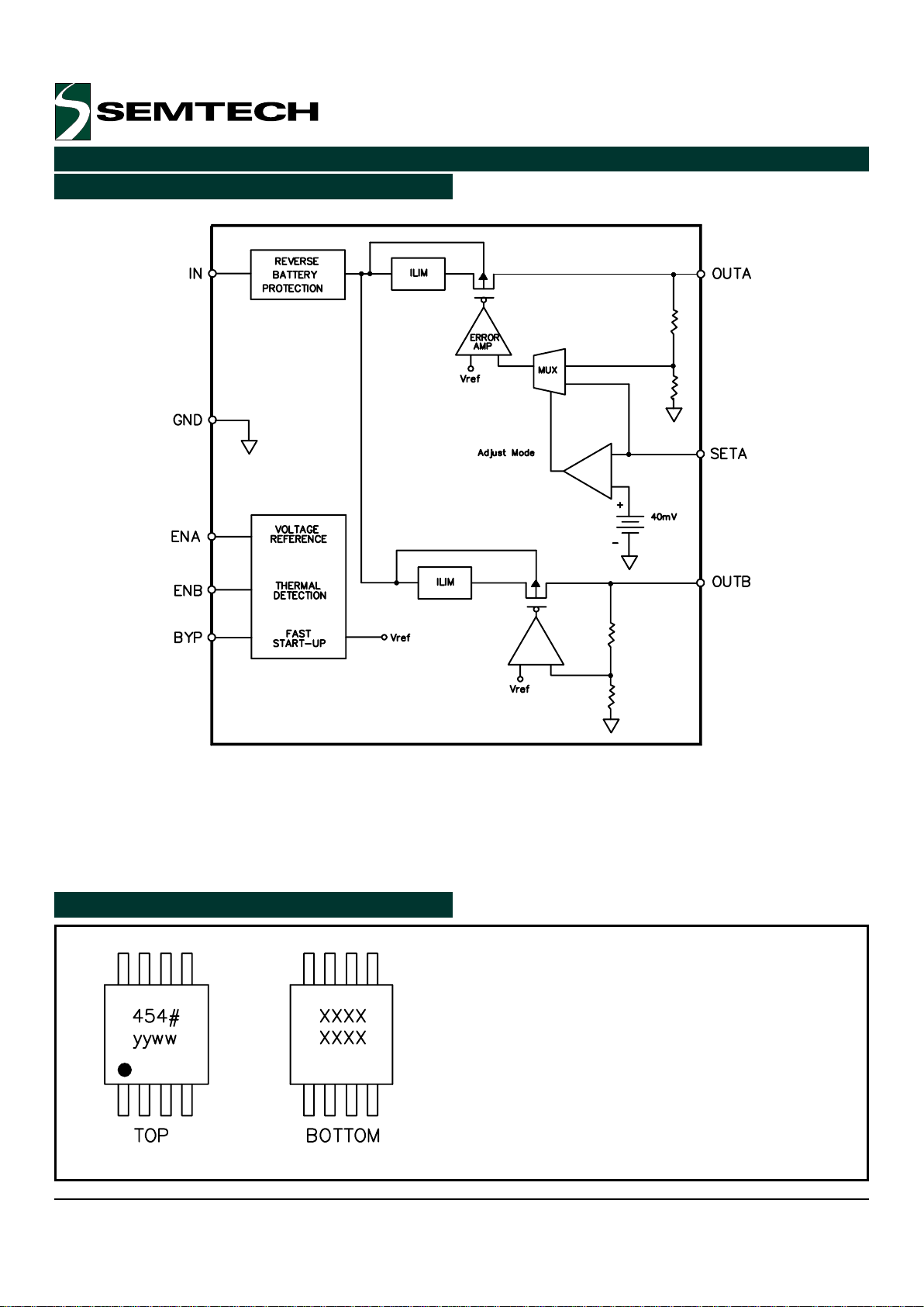
Block Diagram
Marking Information
# = Voltage option (Example: 454F)
yyww = Datecode (Example: 0008)
XXXX = Lot number (Example: E90101-1)

6ã 2000 Semtech Corp. www.semtech.com
SC1454
POWER MANAGEMENT
PIN Descriptions
Applications Information
Theory Of Operation
The SC1454 is intended for applications where very low
dropout voltage, low supply current and low output noise
are critical. Furthermore, the SC1454, by combining two
ultra low dropout (ULDO) regulators, along with enable
controls and output voltage adjustability for one output,
provides a very space efficient solution for multiple
supply requirements.
The SC1454 contains two ULDOs, both of which are
supplied by one input supply, between IN and GND. Each
ULDO has its own active high enable pin (ENA/ENB).
Pulling this pin low causes that specific ULDO to enter a
very low power shutdown state.
The SC1454 contains an internal bandgap reference
which is fed into the inverting input of two error
amplifiers, one for each output. The output voltage of
each regulator is divided down internally using a resistor
divider and compared to the bandgap voltage. The error
amplifier drives the gate of a low R
DS(ON)
P-channel
MOSFET pass device.
Output A has both a fixed and adjustable output voltage
mode. Grounding the SETA pin (pulling it below the Sense/
Select threshold of 40mV) will connect the internal
resistor divider to the error amplifier resulting with the
internally preset output voltage. If SETA is pulled above
this threshold, then the Sense/Select switch will
connect the SETA pin to the error amplifier. Output A will
then be regulated such that the voltage at SETA will equal
V
SETA
, the SETA reference voltage (typically 1.250V).
A bypass pin (BYP) is provided to decouple the bandgap
reference to reduce output noise (on both outputs) and
also to improve power supply rejection.
Each regulator has its own current limit circuitry to
ensure that the output current will not damage the
device during output short, overload or start-up. The
current limit is guaranteed to be greater than 400mA to
allow fast charging of the output capacitor and high
initial currents for DSP initialization.
The SC1454 has a fast start-up circuit to speed up the
initial charging time of the bypass capacitor to enable
the output voltage to come up quicker.
The SC1454 includes thermal shutdown circuitry to turn
off the device if TJ exceeds 150°C (typical), with the
device remaining off until T
J
drops by 20°C (typical).
Reverse battery protection circuitry ensures that the
device cannot be damaged if the input supply is
accidentally reversed, limiting the reverse current to less
than 1.5mA.
Component Selection - General
Output capacitor - Semtech recommends a minimum
capacitance of 1µF at the output with an equivalent
series resistance (ESR) of < 1W over temperature. While
the SC1454 has been designed to be used with ceramic
capacitors, it does not have to be used with ceramic
capacitors, allowing the designer a choice. Increasing the
bulk capacitance will further reduce output noise and
improve the overall transient response.
Input capacitor - Semtech recommends the use of a 1µF
ceramic capacitor at the input. This allows for the device
being some distance from any bulk capacitance on the
rail. Additionally, input droop due to load transients is
reduced, improving overall load transient response.
Bypass capacitor - Semtech recommends the use of a
10nF ceramic capacitor to bypass the bandgap
reference. Increasing this capacitor to 100nF will
further improve power supply rejection. Reducing this
capacitor below 1nF may result in output overshoot at
turn-on.
Component Selection - Externally Setting Output
Referring to the circuit above, the output voltage of
output A can be externally adjusted anywhere within the
range from 1.25V to (V
IN(MAX)
- V
D(MAX)
). The output voltage
will be in accordance with the following equation:
1% tolerance resistors are recommended. The values of
OUTPUT A: 2.5V
OUTPUT B: 2.8V
VIN
ENABLE OUTPUT A
ENABLE OUTPUT B
C3
10nFC41uF
C1
1uFC21uF
R1
100k
R2
100k
U1 SC1454CIMS
1
2
3
4 5
7
6
8
OUTA
OUTB
GND
SETA ENB
ENA
BYP
IN
+•=
2R
1R
1250.1V
OUTA

7ã 2000 Semtech Corp. www.semtech.com
SC1454
POWER MANAGEMENT
impedance allowable to maintain TJ £ 125°C:
This target value can be achieved by using one square
inch of board copper connected to the GND pin (pin 3),
which connects directly to the device substrate.
Increasing this area or the use of multi layer boards will
lower the junction temperature and improve overall
output voltage accuracy.
Layout Considerations
While layout for linear devices is generally not as critical
as for a switching application, careful attention to detail
will ensure reliable operation.
1) Attaching the part to a larger copper footprint will
enable better heat transfer from the device, especially
on PCBs where there are internal ground and power
planes.
2) Place the input, output and bypass capacitors close
to the device for optimal transient response and device
behaviour.
3) Connect all ground connections directly to the ground
plane. If there is no ground plane, connect to a common
local ground point before connecting to board ground.
R1 and R2 should be selected such that the current
flowing through them is ³ 10µA (thus R2 £ 120kW).
Thermal Considerations
The worst-case power dissipation for this part is given
by:
(1)
For all practical purposes, equation (1) can be reduced
to the following expression:
(2)
Looking at a typical application:
V
IN(MAX)
= 4.2V
V
OUTA
= 3V - 2% (worst case) = 2.94V
V
OUTB
= 3.3V - 2% (worst case) = 3.234V
I
OUTA
= I
OUTB
= 150mA
TA = 85°C
Inserting these values into equation (2) above gives us:
Using this figure, we can calculate the maximum thermal
Applications Information (Cont.)
(
)
()
)MAX(Q)MAX(IN
)MAX(OUTB)MIN(OUTB)MAX(IN
)MAX(OUTA)MIN(OUTA)MAX(IN)MAX(D
IV
IVV
IVVP
•+
•−+
•−=
(
)
()
)MAX(OUTB)MIN(OUTB)MAX(IN
)MAX(OUTA)MIN(OUTA)MAX(IN)MAX(D
IVV
IVVP
•−+
•−=
()( )
W334.0
145.0189.0
15.0234.32.415.094.22.4P
)MAX(D
=
+=
•−+•−=
(
)
()
W/C120
334.0
85125
P
TT
)MAX(D
)MAX(A)MAX(J
)MAX(JA
°=
−
=
−
=θ

8ã 2000 Semtech Corp. www.semtech.com
SC1454
POWER MANAGEMENT
Typical Characteristics
Output Voltage vs. Output Current
vs. Junction Temperature, V
OUT
= 2.8V
Output Voltage vs. Junction Temperature
vs. Output Current, V
OUT
= 2.8V
Output Voltage vs. Junction Temperature
vs. Output Current, V
OUT
= 1.5V
Output Voltage vs. Junction Temperature
vs. Output Current, V
OUT
= 5.5V
SETA Reference Voltage vs. Junction Temperature
vs. Output Current, V
IN
= 2.5V
SETA Reference Voltage vs. Junction Temperature
vs. Output Current, VIN = 6.5V
-10.0
-7.5
-5.0
-2.5
0.0
2.5
5.0
7.5
10.0
0 25 50 75 100 125 150
I
OUT
(mA)
V
OUT
Deviation (mV)
VIN = 3.8V
V
OUT
= 2.8V
Top to bottom:
T
A
= 125°C
T
A
= 25°C
T
A
= -40°C
-10.0
-7.5
-5.0
-2.5
0.0
2.5
5.0
7.5
10.0
-50 -25 0 25 50 75 100 125
T
J
(°C)
V
OUT
Deviation (mV)
VIN = 3.8V
V
OUT
= 2.8V
Top to bottom:
I
OUT
= 1mA
I
OUT
= 50mA
I
OUT
= 100mA
I
OUT
= 150mA
-10.0
-7.5
-5.0
-2.5
0.0
2.5
5.0
7.5
10.0
-50 -25 0 25 50 75 100 125
T
J
(°C)
V
OUT
(V)
VIN = 2.5V
V
OUT
= 1.5V
I
OUT
= 150mA
I
OUT
= 1mA
-40
-30
-20
-10
0
10
20
30
40
-50 -25 0 25 50 75 100 125
T
J
(°C)
V
OUT
(V)
VIN = 6.5V
V
OUT
= 5.5V
I
OUT
= 150mA
I
OUT
= 1mA
1.225
1.230
1.235
1.240
1.245
1.250
1.255
1.260
1.265
1.270
1.275
-50 -25 0 25 50 75 100 125
T
J
(°C)
V
SET
(V)
VIN = 2.5V
I
OUT
= 150mA
I
OUT
= 1mA
1.225
1.230
1.235
1.240
1.245
1.250
1.255
1.260
1.265
1.270
1.275
-50 -25 0 25 50 75 100 125
T
J
(°C)
V
SET
(V)
VIN = 6.5V
I
OUT
= 150mA
I
OUT
= 1mA

9ã 2000 Semtech Corp. www.semtech.com
SC1454
POWER MANAGEMENT
Typical Characteristics (Cont.)
Dropout Voltage vs. Output Current
vs. Junction Temperature
Dropout Voltage vs. Junction Temperature
vs. Output Current
Line Regulation vs.
Junction Temperature
Load Regulation vs.
Junction Temperature
Current Limit vs. Junction Temperature
vs. Input Voltage
Off-State Quiescent Current
vs. Junction Temperature
0
25
50
75
100
125
150
175
200
0 25 50 75 100 125 150
I
OUT
(mA)
V
D
(mV)
Top to bottom:
T
J
= 125°C
T
J
= 25°C
T
J
= -40°C
0
25
50
75
100
125
150
175
200
-50 -25 0 25 50 75 100 125
T
J
(°C)
V
D
(mV)
I
OUT
= 150mA
I
OUT
= 50mA
0
1
2
3
4
5
6
7
8
9
10
-50 -25 0 25 50 75 100 125
T
J
(°C)
REG
(LINE)
(mV)
I
OUT
= 1mA
V
IN
= V
OUT
+ 1V to 6.5V
V
IN
= V
OUT
+ 1V to 5.5V
0
1
2
3
4
5
6
7
8
9
10
-50 -25 0 25 50 75 100 125
T
J
(°C)
REG
(LOAD)
(mV)
VIN = V
OUT
+ 1V
I
OUT
= 0.1mA to 150mA
400
450
500
550
600
650
700
750
800
-50 -25 0 25 50 75 100 125
T
J
(°C)
I
LIM
(mA)
VIN = 6.5V
V
IN
= 3.8V
0
50
100
150
200
250
300
350
400
-50 -25 0 25 50 75 100 125
T
J
(°C)
I
Q
(nA)
VIN = 6.5V
V
ENA
= V
ENB
= 0V

10ã 2000 Semtech Corp. www.semtech.com
SC1454
POWER MANAGEMENT
Typical Characteristics (Cont.)
Quiescent Current vs. Junction Temperature
vs. Output Current
Quiescent Current vs. Junction Temperature
vs. Input Voltage
Enable Input Voltage vs. Junction Temperature
vs. Input Voltage
Sense/Select Threshold Voltage vs.
Junction Temperature vs. Input Voltage
Bypass Start-up Rise Time vs. Junction Temperature
vs. Input Voltage
Output Spectral Noise Density vs. Frequency
vs. Bypass Capacitance
0
25
50
75
100
125
150
175
200
-50 -25 0 25 50 75 100 125
T
J
(°C)
I
Q
(µA)
I
OUTA
= I
OUTB
= 150mA
Top to bottom:
V
IN
= 6.5V
V
IN
= 5V
V
IN
= 3.8V
0.4
0.6
0.8
1.0
1.2
1.4
1.6
-50 -25 0 25 50 75 100 125
T
J
(°C)
V
EN
(V)
VIH @ VIN = 6.5V
V
IH
@ VIN = 4V
V
IL
@ VIN = 6.5V
V
IL
@ VIN = 4V
0
10
20
30
40
50
60
70
80
-50 -25 0 25 50 75 100 125
T
J
(°C)
V
TH
(mV)
VIN = 6.5V
V
IN
= 3.8V
0.00
0.25
0.50
0.75
1.00
1.25
1.50
1.75
2.00
-50 -25 0 25 50 75 100 125
T
J
(°C)
t
r
(ms)
C
BYP
= 10nF
V
IN
= 6.5V
V
IN
= 3.8V
0
25
50
75
100
125
150
175
200
-50 -25 0 25 50 75 100 125
T
J
(°C)
I
Q
(µA)
VIN = 6.5V I
OUTA
= I
OUTB
= 150mA
I
OUTA
or I
OUTB
= 150mA
10
100
1000
10000
1.E+01 1.E+02 1.E+03 1.E+04 1.E+05 1.E+06
f (Hz)
e
n
(nV/
√
Hz)
C
BYP
= 10nF
C
BYP
= 100nF
V
IN
= 2.8V
V
OUT
= 1.8V
I
OUT
= 50mA
C
IN
= 1µF
C
OUT
= 2.2µF
T
A
= 25°C

11ã 2000 Semtech Corp. www.semtech.com
SC1454
POWER MANAGEMENT
Typical Characteristics (Cont.)
Output Spectral Noise Density vs. Frequency
vs. Output Capacitance
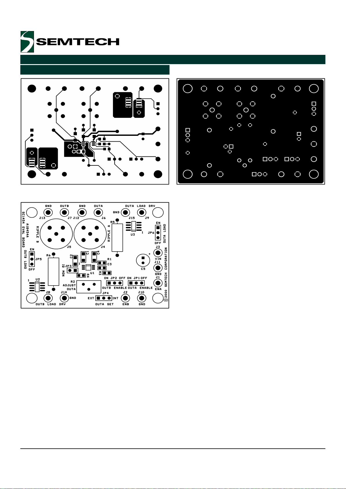
Evaluation Board Schematic
R2
1
3
2
R4
JP4
OUTA SET
1
2
3
+
C5
220uF
C3 C4
C2
C1
JP5
OUTB LOAD
1
2
3
JP6
OUTA LOAD
1
2
3
J15
GND
J14
GND
J13
GND
J12
GND
J11
GND
J10
GND
U1
SC1454xIMS
1
2
3
4 5
7
6
8
OUTA
OUTB
GND
SETA ENB
ENA
BYP
IN
J9
OUTA LOAD DRV
J8
OUTB LOAD DRV
JP3
IQ MON
1
2
JP1
OUTA ENABLE
1
2
3
J1
ENA
JP2
OUTB ENABLE
1
2
3
J3
VIN
J2
ENB
J4
RIPPLE A
12345
J5
RIPPLE B
12345
R1
R3
J7
OUTB
J6
OUTA
R6
R5
U3
Si4410
1
2
3
4
5
6
7
8
S
S
SGDD
D
D
U2
Si4410
1
2
3
45
6
7
8
S
S
SGDD
D
D
EN
EN
OFF
OFF
INT
EXT
ON ON
OFF OFF
1
10
100
1000
10000
1.E+01 1.E+02 1.E+03 1.E+04 1.E+05 1.E+06
f (Hz)
e
n
(nV/
√
Hz)
C
OUT
= 2.2µF
C
OUT
= 10µF
V
IN
= 2.8V
V
OUT
= 1.8V
I
OUT
= 50mA
C
IN
= 1µF
C
BYP
= 10nF
T
A
= 25°C
12ã 2000 Semtech Corp. www.semtech.com
SC1454
POWER MANAGEMENT
Evaluation Board Gerber Plots
Top Copper Bottom Copper
Top Assembly

13ã 2000 Semtech Corp. www.semtech.com
SC1454
POWER MANAGEMENT
ytitnauQecnerefeRnoitpircseD/traProdneVsetoN
22C,1CcimarecFµ2.2ataruM61K522R7X6-24MRG
13CcimarecFn01suoiraV
14CcimarecFµ1ataruM52K501R7X6-24MRG
15CV01,Fµ022suoiraV
22J,1JniptseTsuoiraVetihW
37J,6J,3JniptseTsuoiraVdeR
25J,4JtekcosCNBsuoiraVV
TUO
rotinomelppir
29J,8JniptseTsuoiraVegnarO
651J-01JniptseTsuoiraVkcalB
56PJ-4PJ,2PJ,1PJnip3,redaeHsuoiraV
13PJnip2,redaeHsuoiraV
23R,1Rk01 W W01/1,suoiraV
12Rk052 W T52,snruoBretemoitnetopremmirT
14Rk26 W W01/1,suoiraV
26R,5RdaolAm051suoiraVeulavemasebtonyam,W1
11U SMIx4541CS hcetmeS
23U,2U0144iSyahsiV
Evaluation Board Bill Of Materials

14ã 2000 Semtech Corp. www.semtech.com
SC1454
POWER MANAGEMENT
Semtech Corporation
Power Management Products Division
652 Mitchell Rd., Newbury Park, CA 91320
Phone: (805)498-2111 FAX (805)498-3804
Outline Drawing - MSOP-8
Contact Information
Land Pattern - MSOP-8
 Loading...