


LOW VOLTAGE, BOOST DC-DC
CONTROLLER
SC1408
August 22, 2000
TEL:805-498-2111 FAX:805-498-3804 WEB:http://www.semtech.com
DESCRIPTION
The SC1408 is a low voltage boost controller that operates from a 1.8V to 16.5V input range. A shutdown pin
allows the user to turn the controller off reducing supply current to less than 2µA typical. Output voltage can
be preset to 5V or is adjustable from 3V to 16.5V with
a resistor divider. The controller changes frequency in
low load conditions to improve efficiency.
The SC1408 was designed for two cell Alkaline or single cell Lithium Ion battery applications. With the
proper external components it can be used as a boost
converter or a buck/boost converter.
A current sense is implemented with an external resistor that is not in the load current path.
The SC1408 operates in “bootstrapped” mode. When
the input voltage to the device is less than 2.5V during
startup, a low voltage 50% fixed duty cycle oscillator is
switched in to initiate boost action.
FEATURES
•= 1.8V to 16.5V input range
•= Up to 10W output power
•= Preset 5V or adjustable output
•= Up to 300kHz switching frequency
•= 10µA max shutdown current
•= Industrial temperature range
•= SO-8 or MSOP-8 package
APPLICATIONS
PDA Power supplies
•=
•= Battery powered applications
•= Positive LCD Bias generator
•= Portable communications (cellular phones)
•= Peripheral card supplies
•= Industrial power supplies
ORDERING INFORMATION
Part Number
SC1408IS.TR SO-8 -40° to +85°C
(1)
Package Temp. Range (TA)
SC1408IMS.TR MSOP-8
Note:
(1) Only available in tape and reel packaging. A reel
contains 2500 devices.
TYPICAL APPLICATION - BOOST CONFIGURATION
U1
2
4
SHDN
5
REF
7
GND
SC1408IS
L1
GATEBST
ISENSE
FB
AGND
1
8
3
6
Vin (1.8V to 16.5V) Vout (3V to 16.5V)
+
C2
C5
Q1
R2
D1
R3
R4
+
C3
1
© 2000 SEMTECH CORP. 652 MITCHELL ROAD NEWBURY PARK CA 91320

LOW VOLTAGE, BOOST DC-DC
SC1408
CONTROLLER
August 22, 2000
ABSOLUTE MAXIMUM RATINGS
Parameter Symbol Maximum Units
Input Voltage BST to GND -0.3 to 18 V
Small Signal Ground to Power Ground GND to AGND ±0.1 V
GATE to GND -0.3 to VBST+0.3 V
FB, SHDN, REF, ISENSE to GND -0.3 to min. of VBST+0.3 or 5 V
Operating Temperature T
Junction Temperature Range T
Storage Temperature T
Lead Temperature (Soldering) 10 seconds T
Thermal Resistance, Junction to Ambient
SO-8
θ=JA
MSOP-8
Thermal Resistance, Junction to Case
SO-8/MSOP-8
ELECTRICAL CHARACTERISTICS
Unless specified: V
OUT
= 5V; I
= 0mA; TA = +25°C
LOAD
(1)
θ=JC
PARAMETER SYM CONDITIONS MIN TYP MAX UNITS
Input Voltage T
T
Supply Current V
= 16.5V,
OUT
= 25°C 1.8 16.5 V
A
= -40°C to +85°C 1.8 16.5 V
A
SHDN ≤=0.4V
V
= 10V,
OUT
1.6V ≤=SHDN ≤=5V
A
J
STG
L
-40 to +85 °C
-40 to +150 °C
-65 to +160 °C
+300 °C
165
°C/W
206
40 °C/W
TA = -40°C to +85°C 110 140 uA
TA = -40°C to +85°C 2 10 µA
Output Voltage V
Load Regulation V
Line Regulation V
= 2.0V to 5.0V, TA = -40°C to +85°C 4.800 5.0 5.200 V
IN
= 2.0V, V
IN
= 2.7V to 4.0V, V
IN
OUT
= 5V, I
OUT
= 0mA to 500mA 60 mV/A
LOAD
= 5V, I
= 500mA 7 mV/V
LOAD
Minimum Start Up Voltage No load 1.8 V
Maximum Swit ch On Time T
Minimum Switch Of f Time T
Efficiency V
Reference Voltage V
ON
OFF
REF
= 4V, V
IN
I
= 0µA TA = -40°C to +85°C 1.176 1.200 1.224 V
REF
OUT
Reference Load Regulation 0µA <
Reference Line Regulation 5V <
FB Trip Point Voltage V
FB Input Current I
FM
FB
= -40°C to +85°C 1.176
T
A
= -40°C to +85°C
T
A
= 5V, I
I
< 100µA -4 10 mV
REF
V
OUT
= 500mA 87 %
LOAD
< 16.5V 40 100 µV/V
TA = 25°C
TA = 25°C
9.6 16 22.4 µs
1.4 2.3 3.2 µs
1.200
V
1.224
-4
nA
+ 40
2
© 2000 SEMTECH CORP. 652 MITCHELL ROAD NEWBURY PARK CA 91320

August 22, 2000
ELECTRICAL CHARACTERISTICS
LOW VOLTAGE, BOOST DC-DC
CONTROLLER
(1)
SC1408
Unless specified: V
OUT
= 5V; I
= 0mA; TA = +25°C
LOAD
PARAMETER SYM CONDITIONS MIN TYP MAX UNITS
SHDN Input High Voltage V
SHDN Input Low Voltage V
SHDN Input Current I
Current Limit Trip Level V
ISENSE Input Current I
IH
IL
IN
CS
SENSE
V
OUT
GATE Rise Time V
GATE Fall Time V
= 3V to 16.5V TA = 25°C
V
= 2.7V to 16.5V 1.6 V
OUT
V
= 2.7V to 16.5V 0.4 V
OUT
V
= 16.5V, SHDN = 0V or 5V + 1µA
OUT
8580100 115
= -40°C to +85°C
T
A
120
0.01 + 1µA
= 5V, 1nF from GATE to GND 50 ns
OUT
= 5V, 1nF from GATE to GND 50
OUT
GATE On Resistance GATE = high or low 15 30
NOTE:
(1) This device is ESD sensitive. Use of standard ESD handling precautions is required.
mV
Ω
3
© 2000 SEMTECH CORP. 652 MITCHELL ROAD NEWBURY PARK CA 91320

August 22, 2000
BLOCK DIAGRAM
LOW VOLTAGE, BOOST DC-DC
CONTROLLER
SC1408
1.20V
REFERENCE
TRIG Q
MAX ON TIME
ONE SHOT
AGND
16uS
ERROR
COMP
+
-
MIN OFF TIME
ONE SHOT
TRIG Q
2.3uS
REF
S
R
LOW
VOLTAGE
OSCILLATOR
Q
MODE
DETECT
+
CURRENT
SENSE AMP
START
UP
COMP
FB
INTERNAL BIAS
50mV
BIAS
+
SHDN
BST
-
2.5V
GATE
GND
+
ISENSE
-
0.1V
PIN CONFIGURATION
PIN DESCRIPTION
Pin # Pin Name Pin Function
Top View
1 GATE Gate drive output.
2 BST Supply voltage.
3 FB Voltage feedback.
4 SHDN Logic high shuts down the converter.
5 REF Reference output pin.
6 AGND Small signal analog and digital ground.
(SO-8/MSOP-8)
7 GND Power ground.
8 ISENSE Current sense pin.
4
© 2000 SEMTECH CORP. 652 MITCHELL ROAD NEWBURY PARK CA 91320

LOW VOLTAGE, BOOST DC-DC
CONTROLLER
August 22, 2000
Fig. 1: Typical Application - Boost Configuration
SC1408
Vin=3.3V
C2
100uF
L1 22uH
COILCRAFT DO3316P-223
U1
FB
12
8
3
67
GATEBST
4
+
SHDN
5
REF
ISENSE
AGNDGND
C5
SC1408IS
D1
B130T
Q1
IRLR024N
R2
0.05Ohm
R3
31.6k
R4
10.0k
0.1uF
(1) See Component Selection
Fig. 2: Typical Application - Buck/Boost (SEPIC) Configuration
D2 1N4148
C9
(1)
+
C3
100uF
Vout=5V
+
C8
100uF
Vin=2.7V to 6V
C2
+
100uF
C4
0.1uF
L1A 22uH
U1
4
5
C5
0.1uF
L1A/L1B IS COUPLED INDUCTOR
PULSE PE-53718 OR
EQUIVALENT
SHDN
REF
SC1408IS
ISENSE
AGNDGND
12
12
GATEBST
8
3
FB
67
C1
+
Q1
IRLL3303
R2
0.05Ohm
100uF
D1
B130T
R3
31.6k
4
L1B
22uH
3
(1) See Component Selection
R4
10.0k
C9
(1)
+
C3
100uF
Vout=5V
+
C8
100uF
5
© 2000 SEMTECH CORP. 652 MITCHELL ROAD NEWBURY PARK CA 91320

LOW VOLTAGE, BOOST DC-DC
CONTROLLER
August 22, 2000
Fig. 3: Achieving output voltages greater than 16.5V
SC1408
D4
1N4148
R6 470
L1 22uH
3.3V IN
U1
Q1
IRL3103S
C2
100uF
FB
12
8
3
67
GATEBST
C4
0.1uF
+
4
SHDN
5
REF
ISENSE
AGNDGND
SC1408IS
D3
C5
0.1uF
12V
Fig. 4: Implementing shutdown with input/output isolation
D1
B130T
200k
R2
0.05Ohm
R3
R4
10.0k
+
C3
100uF
25V OUT
+
C8
100uF
Q2
SHORT = RUN
OPEN = SHUTDOWN
3.3V IN
J1
R5
5.1k
1
2
Si2301DS
C2
100uF
C4
0.1uF
+
C5
0.1uF
4
5
L1 22uH
U1
SHDN
REF
SC1408IS
GATEBST
ISENSE
AGNDGND
FB
D1
B130T
R3
12
8
3
67
Q1
IRLL3303
R2
0.05Ohm
90k
R4
10.0k
+
C3
100uF
12V OUT
+
C8
100uF
6
© 2000 SEMTECH CORP. 652 MITCHELL ROAD NEWBURY PARK CA 91320

August 22, 2000
LOW VOLTAGE, BOOST DC-DC
CONTROLLER
SC1408
THEORY OF OPERATION
The SC1408 is a modified hysteretic boost converter
controller. The power switch is turned on when the output voltage falls slightly below it’s setpoint. It remains on
for approximately 16µs, or until the inductor current
reaches limit, whichever occurs first. The power switch is
then turned off for 2.3µs, or until the output voltage once
again falls below setpoint, whichever occurs last.
The SC1408 is normally powered from the output voltage. Internal circuitry, such as the bandgap, comparators and one shots will not function properly until the BST
pin voltage reaches 2.5V. To ensure startup at low input
voltages, the normal control circuitry is disabled and a
special, low voltage start up oscillator generates an approximate square wave at the GATE pin, initiating boost
action. When the output voltage reaches 2.5V, the normal control circuitry is enabled and the start up oscillator
shuts down.
To conserve power, a SHDN pin is provided which,
when pulled high, shuts down most internal circuitry. The
output voltage will then be one diode drop below the input.
COMPONENT SELECTION
Boost Converter
SENSE
R
The value of the sense resistor is the primary determining factor for maximum output current. The SC1408 has
a fixed current limit voltage threshold, which is developed by the peak inductor current flowing through
SENSE. RSENSE may be determined either from the maxi-
R
mum output current curves or from the equation below:
æ
V
CS
I
)MAX(O
R
−
ç
1
−=
ç
SENSE
è
æ
t
()( )
ç
ç
L2
è
−+
:Where
=
F
=
FET
ö
VVV
−+
INFO
÷
÷
VVV
−+
FETFO
ö
VVVVV
−+−
INFOFETINoff
VVV
FETFO
Drop VoltageForward Diode Output V
SENSE
pin to GND, or to any voltage in the 3.0V to 16.5V range
using external divider resistors.
The bottom resistor in the divider chain (R4) should be
300kΩ or less and the top resistor (R3 in the application
circuits) can be calculated from:
æ
ç
4R3R
ç
V
è
V
REF
ö
O
−= 1
Inductor
The SC1408 will work with a wide range of inductor values. A good choice for most applications is 22µH.
Smaller inductor values result in higher peak currents
and increased output ripple, while larger values will result in slower loop response.
Transistor Selection
Normally the power switch will be an N-channel MOSFET, although in certain circumstances an NPN bipolar
may be substituted.
The choice of FET can be critical, especially in battery
powered applications where the converter must be able
to use all of the available energy in the battery. This requires that the converter be capable of starting up from
very low input voltages. For example a two cell alkaline
system’s terminal voltage will drop to 1.8V as it approaches full discharge. For these demanding applications, a FET with low V
thumb is that V
should be at least 0.5V less than the
GS(th)
is required. A good rule of
GS(th)
minimum input voltage.
Diode
For most applications, a Schottky diode should be used
as the output rectifier. It will be subjected to reverse voltages of at least V
, and average current will be equal to
O
the output current. Industry standard 1N5817 series or
an equivalent surface mount part would be suitable.
Output Capacitors
Output capacitors should be low ESR to minimize ripple
voltage and maximize efficiency. Low ESR tantalums,
OSCONs or the newer Polymer capacitors should be
DCR Inductor and R FET, across VoltageV
used. Ripple voltage will be approximately:
In the equation above, the use of 2.3µs for t
to slightly optimistic current values for low V
The theoretical curves use the actual value of t
=0.5V, V
V
F
=0.3V and VCS=0.08V and are generated
FET
for L=22µH.
may lead
off
ratios.
O/VIN
,
off
R*V
V =
RIPPLE
R
ESRCS
SENSE
Input Capacitors
Input capacitors on a boost converter are less critical
than the output capacitors, since there are no fast cur-
Output Voltage
Output voltage can be set to 5V by connecting the FB
rent pulses drawn from the input supply. A 100µF tantalum will be adequate for most applications.
7
© 2000 SEMTECH CORP. 652 MITCHELL ROAD NEWBURY PARK CA 91320

August 22, 2000
LOW VOLTAGE, BOOST DC-DC
CONTROLLER
SC1408
Feed Forward Capacitor
Although converters based on the SC1408 are stable,
with no possibility of oscillation, they are susceptable to
“mode switching” at intermediate current levels. This
leads to increased ripple voltage and slightly reduced
efficiency. Mode switching can be eliminated by a suitable choice of C9. It is possible to empirically select C9.
Start with a value of about 100pF and adjust until all low
frequency output ripple is eliminated at the desired output current.
See AN99-15 “SC1408 Operating Modes” for a full discussion of the origins of “Mode switching” and a more
analytical approach to the selection of C9.
COMPONENT SELECTION
SEPIC Converter
SENSE
R
Again, with the SEPIC topology, the value of the sense
resistor is the primary determining factor for maximum
output current. The simplest approach to select R
is to add Vin to Vo and use this value as the output voltage in the output current curves or in the equation for
Boost converter.
Output Voltage
Output voltage setting works exactly the same in SEPIC
topology as in Boost, including the ability to set to 5V by
connecting the FB pin to GND. Care must be taken to
ensure that the IC supply (pin2; BST) does not exceed
its 16.5V rating. In the circuit of Fig.2: This requires maximum output voltage to be limited to 16.5V-Vin. Higher
output voltages are possible with different IC supply
strategies.
Inductor
The SEPIC topology requires a coupled inductor. Again
a good choice for most applications is 22uH. Smaller inductor values result in higher peak currents and increase
output ripple, while larger values will result in slower loop
response.
Transistor Selection
The choice of FET can be critical, especially in battery
powered applications where the converter must be able
to use all of the available energy in the battery. This requires that the converter be capable of starting up from
very low input voltages. For example a two cell alkaline
system’s terminal voltage will drop to 1.8V as it approaches full discharge. For these demanding applications, a FET with low V
thumb is that V
should be at least 0.5V less than the
GS(th)
is required. A good rule of
GS(th)
minimum input voltage.
SENSE
Diode
For most applications, a Schottky diode should be used
as the output rectifier. It will be subjected to reverse voltages of at least V
and average current equal to the
O +VIN
output current. Industry standard 1N5817 series or an
equivalent surface mount part would be suitable.
Output Capacitors
Output capacitors should be low ESR to minimize ripple
voltage and maximize efficiency. Low ESR tantalums,
OSCONs or the newer Polymer capacitors should be
used.
Input Capacitors
Input capacitors on a SEPIC converter are less critical
than the output capacitors, since there are no fast current pulses drawn from the input supply. A 100µF tantalum will be adequate for most applications.
Series Capacitors
The Series capacitor(s) must be capable of handling an
RMS current given by:-
5.0VII+
O
=
ORMS
V
IN
Feed Forward Capacitor
The feed forward capacitor should be selected in the
same way as for a Boost application.
LAYOUT GUIDELINES
The SC1408 is fairly insensitive to layout, however following some simple guidelines will help ensure successful implementation.
Whenever possible, lay the circuitry out over a ground
plane. Connect AGND and GND together at the IC and
return to the ground plane with one or two vias. Place
the current sense resistor (R2), the REF decoupling capacitor (C5) and the divider resistors (R3 and R4) close
to the IC, Return the ground side of these components
to the ground plane close to the AGND/GND pin vias.
Connect the top side of the sense resistor to ISENSE
with a short trace and the source of Q1 directly to the
sense resistor. Make the output loop Q1, D1 and the
output capacitors (C3, C8) as small as possible to minimize EMI.
8
© 2000 SEMTECH CORP. 652 MITCHELL ROAD NEWBURY PARK CA 91320

LOW VOLTAGE, BOOST DC-DC
CONTROLLER
August 22, 2000
3.5
3.0
2.5
Vo=3.3V
L=22uH
20mOhm
25mOhm
2.0
Io (A)
1.5
1.0
0.5
35mOhm
50mOhm
100mOhm
0.0
2.0 2.2 2.4 2.6 2.8 3.0 3.2
3.5
Vo=12V
3.0
L=22uH
2.5
2.0
Io (A)
1.5
1.0
0.5
0.0
2.0 4.0 6.0 8.0 10.0 12.0
Vin (V)
20mOhm
25mOhm
35mOhm
50mOhm
100mOhm
Vin (V)
Figs. 5 - 8: Maximum output current vs. input voltage and sense resistor value. (Boost Mode)
3.5
Vo=5V
L=22uH
3.0
2.5
2.0
Io (A)
1.5
1.0
0.5
0.0
2.0 2.5 3.0 3.5 4.0 4.5 5.0
4.0
Vo=15V
3.5
L=22uH
3.0
2.5
2.0
Io (A)
1.5
1.0
0.5
0.0
2.0 4.0 6.0 8.0 10.0 12.0 14.0 16.0
Vin (V)
Vin (V)
SC1408
20mOhm
25mOhm
35mOhm
50mOhm
100mOhm
20mOhm
25mOhm
35mOhm
50mOhm
100mOhm
100%
Vo=5V
90%
80%
Efficiency (%)
70%
60%
1 10 100 1000
100%
Vo=15V
90%
80%
Efficiency (%)
70%
60%
1 10 100 1000
Io (mA)
Io (mA)
Vin=5.0V
Vin=4.0V
Vin=3.3V
Vin=3.0V
Vin=12V
Vin=9.0V
Vin=5.0V
Vin=3.0V
Vin=1.8V
100%
Vo=12V
90%
80%
Efficiency (%)
70%
60%
1 10 100 1000
Io (mA)
Vin=5.0V
Vin=3.0V
Vin=1.8V
Figs. 9-11:Efficiency in the Boost Application circuit of Fig.1
9
© 2000 SEMTECH CORP. 652 MITCHELL ROAD NEWBURY PARK CA 91320

August 22, 2000
LOW VOLTAGE, BOOST DC-DC
CONTROLLER
SC1408
Output Ripple Voltage; Vin=3V, Vo=5V, Io=470mA
Ch1 = Output Ripple
Ch2 = Voltage at GATE pin
Output Ripple Voltage; Vin=3V, Vo=5V, Io=810mA
Ch1 = Output Ripple
Ch2 = Voltage at GATE pin
Load Transient; Vin=3V, Vo=5V, Io=0 to 500mA
Ch1 = Output Voltage
Ch2 = Load Current (0.5A/div)
© 2000 SEMTECH CORP. 652 MITCHELL ROAD NEWBURY PARK CA 91320
Load Transient; Vin=2V, Vo=5V, Io=0 to 500mA
Ch1 = Output Voltage
Ch2 = Load Current (0.5A/div)
10

August 22, 2000
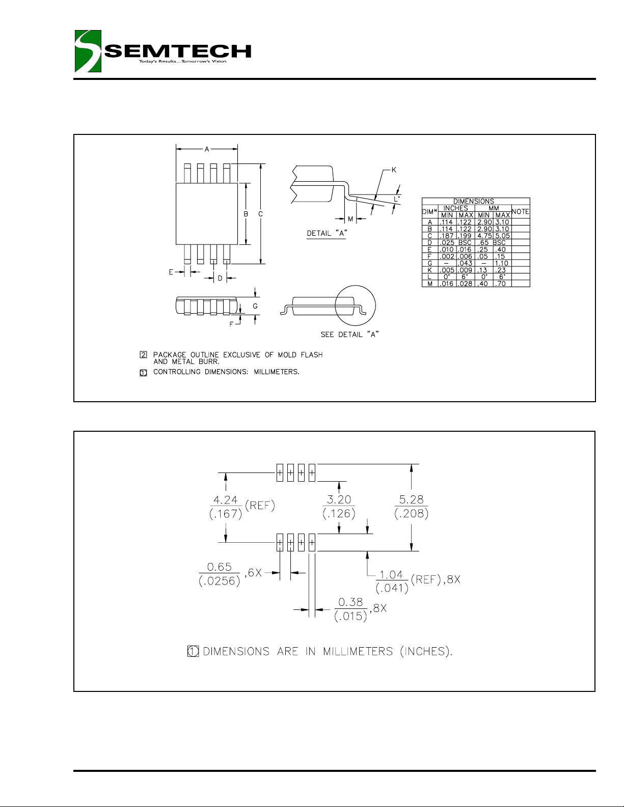
OUTLINE DRAWING - SO-8
LOW VOLTAGE, BOOST DC-DC
CONTROLLER
SC1408
JEDEC
REF: MS-012AA
LAND PATTERN - SO-8
11
© 2000 SEMTECH CORP. 652 MITCHELL ROAD NEWBURY PARK CA 91320
August 22, 2000
OUTLINE DRAWING - MSOP-8
LOW VOLTAGE, BOOST DC-DC
CONTROLLER
SC1408
LAND PATTERN - MSOP-8
ECN00-1275
12
© 2000 SEMTECH CORP. 652 MITCHELL ROAD NEWBURY PARK CA 91320
 Loading...