


SINK AND SOURCE DC/DC CONTROLLER FOR
TERMINATION POWER SUPPLY APPLICATIONS
SC1110
PRELIMINARY - October 9, 2000
TEL:805-498-2111 FAX:805-498-3804 WEB:http://www.semtech.com
DESCRIPTION
The SC1110 is a low-cost, full featured, synchronous
voltage-mode controller designed to generate termination voltage in double data rate (DDR) memory systems and other applications where wide data bus need
to be actively terminated. Synchronous control of the
MOSFET half bridge allows power flowing bidirectionally. The termination voltage can be tightly
regulated to track the chipset voltage, i.e. to be exactly
50% of that at all times.
The SC1110 is ideal for low cost implementation of termination voltage supplies. SC1110 features include
temperature compensated voltage reference, triangle
wave oscillator and current sense comparator circuitry,
and allows the use of inexpensive N-channel power
switches.
The SC1110 operates at a fixed 250kHz, providing an
optimum compromise between efficiency, transient
performance, external component size, and cost.
FEATURES
•= Generates termination voltages for active termina-
tion schemes
•= 1% set point accuracy
•= For ±7A output current, transient regulation is bet-
ter than ±80mV
•= V
•= Buffered V
•= R
pin available
REFIN
sensing for over current protection in hiccup
DSON
for system usage
REFOUT
mode
•= Soft start and logic input enabling
•= 250kHz switching for best transient and efficiency
performance
•= Gate drive capable for 0.5A sourcing and sinking
APPLICATIONS
•= For DDR memory systems
•= For active termination schemes in high speed logic
systems
ORDERING INFORMATION
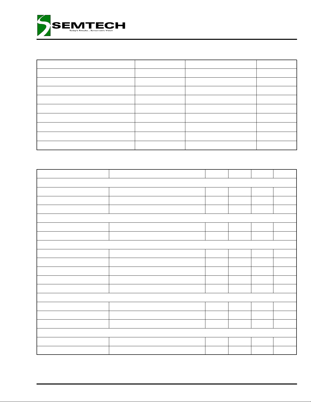
DEVICE
(1)
PACKAGE TEMP. RANGE (TJ)
TYPICAL APPLICATION CIRCUIT
REFOUT
SS/ENBL
PWRGD
C1
R1
5k
R2
0.01
1.24k
C3
0.1
C25
0.1
R3
10
C2
0.1
U1
SC1110
1
VCC
2
SS/ENBL
3
OCSET
4
PWRGD
5
GND
6
PHASE
7
DL
C10-14: Sanyo, 4SP560M
C8,9,15-24: TDK, CC3216AX5R0J106K
L1: Panasonic, ETQP6F0R8L or Falco, QPIP1205-809-3
Q1,Q2 options: Si9426DY, FDS6890A, IRF7401
D1: ON Semi (Motorola)
REFOUT
REFIN
SENSE
COMP
BSTL
BSTH
SC1110CSTR SO-14 0 - 125°C
Note:
(1) Only available in tape and reel packaging. A reel
contains 2500 devices.
+5Vcc
+
C10,11
C8,9
Q1
Si9426DY
Q2
Si9426DY
C7
1.0
C6
1.0
2 x 10uF
800 nH
L1
C12-14
3 x 560uF
2 x 560uF
R4
C4
1k
14
13
12
11
10
9
8
DH
0.022
R5
1k
C5
R6
0.047
4.7k
D1
MBRM120
R7
2.2
R8
2.2
C15-24
10 x 10uF
Vin 2.5V
_
+
Vout = 1.25V @ 7A
_
1
© 2000 SEMTECH CORP. 652 MITCHELL ROAD NEWBURY PARK CA 91320
SINK AND SOURCE DC/DC CONTROLLER FOR
SC1110
TERMINATION POWER SUPPLY APPLICATIONS
PRELIMINARY - October 9, 2000
ABSOLUTE MAXIMUM RATINGS
Parameter Symbol Maximum Units
V
, BSTL to GND V
CC
IN
PGND to GND ± 0.5 V
PHASE to GND -0.5 to 18 V
BSTH to PHASE 14 V
-0.5 to 14 V
Thermal Resistance Junction to Case
Thermal Resistance Junction to Ambient
Operating Temperature Range T
Storage Temperature Range T
Lead Temperature (Soldering) 10 sec T
θ
JC
θ
JA
STG
LEAD
A
45 °C/W
115 °C/W
0 to 70 °C
-65 to +150 °C
300 °C
ELECTRICAL CHARACTERISTICS
Unless specified: VCC = 4.75V to 12.6V; GND = PGND = 0V; FB = VO; V
PARAMETER CONDITIONS MIN TYP MAX UNITS
POWER SUPPLY
Supply Voltage V
Supply Current EN = V
Line Regulation V
= 2.5 ± 0.5V, VO = VIN/2 @ 0A 0.5 %
IN
CC
CC
UNDER VOLTAGE LOCKOUT
Turn-On Threshold TBD 4.2 TBD V
Turn-Off Threshold TBD 4.0 TBD V
ERROR AMPLIFIER
Transconductance 2 mS
BSTL
= 12V; V
BSTH-PHASE
= 12V; TJ = 25oC
4.4 12.6 V
8mA
Open Loop DC Gain 50 dB
Bandwidth -3dB 500 kHz
COMP Source Capability ±250 µA
Input Bias 58µA
OSCILLATOR
Oscillator Frequency 225 250 275 kHz
Oscillator Max Duty Cycle 90 95 %
Ramp Height 1V
TIMING
Minimum Off-Time 100 ns
Dead Time 80 ns
2
© 2000 SEMTECH CORP. 652 MITCHELL ROAD NEWBURY PARK CA 91320

SINK AND SOURCE DC/DC CONTROLLER FOR
SC1110
TERMINATION POWER SUPPLY APPLICATIONS
PRELIMINARY - October 9, 2000
ELECTRICAL CHARACTERISTICS
Unless specified: VCC = 4.75V to 12.6V; GND = PGND = 0V; FB = VO; V
PARAMETER CONDITIONS MIN TYP MAX UNITS
MOSFET DRIVERS
Peak DH Sink/Source Current BSTH - DH = 4.5V, DH - PHASE = 3.0V 0.5 A
DH - PHASE = 1.5V 0.1
Peak DL Sink/Source Current BSTL - DL = 4.5V, DL - GND = 3.0V 0.5 A
DL - GND = 1.5V 0.1
PROTECTION
BSTL
= 12V; V
BSTH-PHASE
= 12V; TJ = 25oC
Over Current Set Isource V
= 4.5V 180 200 220 µA
OCSET
SOFT START
Charge Current V
Discharge Current V
= 1.5V 10 µA
SS
= 1.5V 2 µA
SS
POWER GOOD
Upper Threshold 112 %
Lower Threshold 88 %
PWRGD Voltage Low I
= 2mA 0.5 V
PWRGD
REFERENCE
REFOUT Source Current 3 mA
Input Bias 58µA
NOTE:
(1) Specification refers to application circuit (Figure 1.).
BLOCK DIAGRAM
3
© 2000 SEMTECH CORP. 652 MITCHELL ROAD NEWBURY PARK CA 91320
PRELIMINARY - October 9, 2000
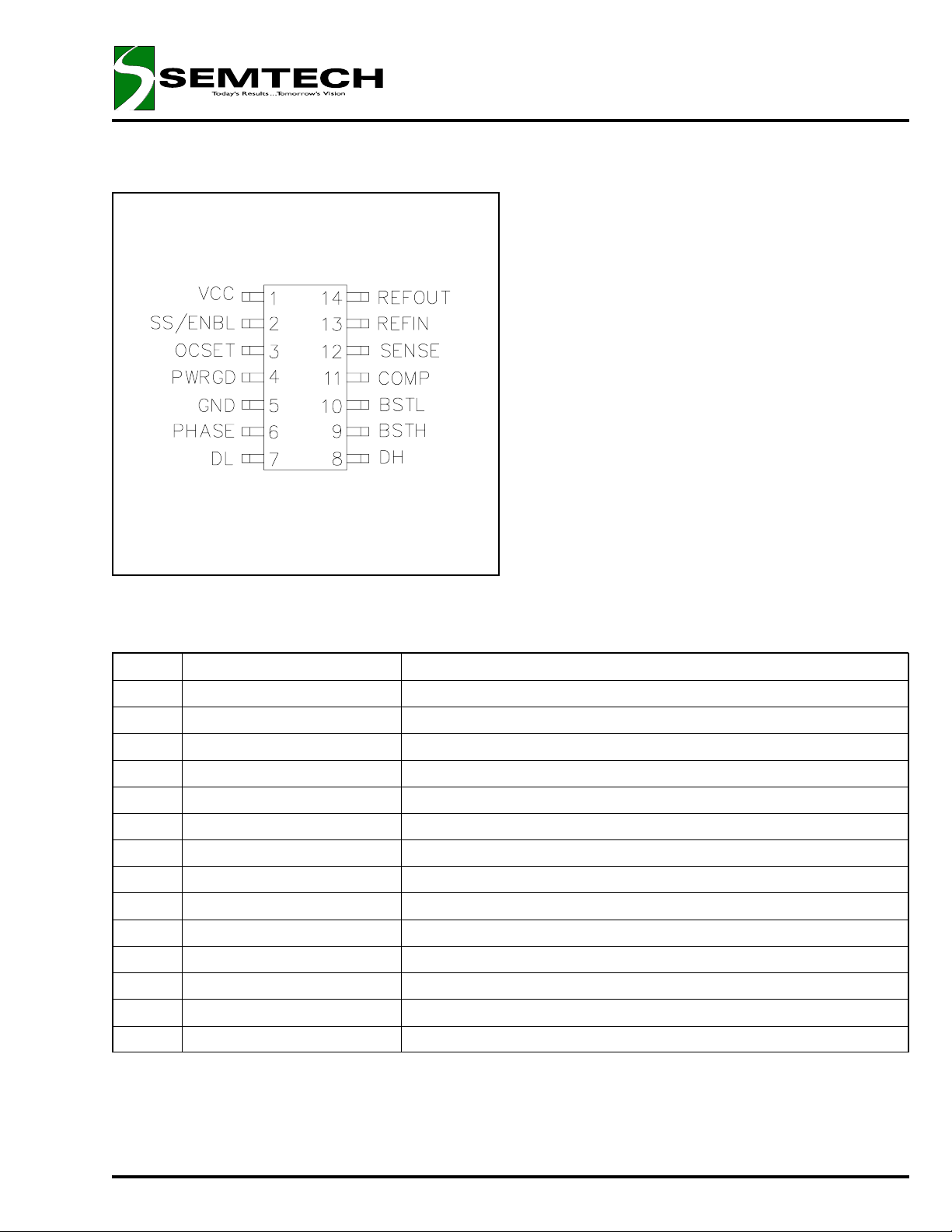
PIN CONFIGURATION
Top View
(14-Pin SOIC)
SINK AND SOURCE DC/DC CONTROLLER FOR
TERMINATION POWER SUPPLY APPLICATIONS
SC1110
PIN DESCRIPTION
Pin # Pin Name Pin Function
1 VCC Chip supply voltage.
2 SS/ENBL Soft start/Enable.
3 OCSET Current limit set point.
4 PWRGD Logic high indicates correct output.
5 GND Ground.
6 PHASE Phase node connection between MOSFET’s.
7 DL Low side driver output.
8 DH High side driver output.
9 BSTH High side drive supply.
10 BSTL Low side drive supply.
11 COMP Error amplifier output, compensation.
12 SENSE Error amplifier negative input.
13 REFIN Error amplifier positive input.
14 REFOUT Buffered reference voltage.
NOTE:
(1) All logic level inputs and outputs are open collector TTL compatible.
4
© 2000 SEMTECH CORP. 652 MITCHELL ROAD NEWBURY PARK CA 91320

SINK AND SOURCE DC/DC CONTROLLER FOR
TERMINATION POWER SUPPLY APPLICATIONS
PRELIMINARY - October 9, 2000
THEORY OF OPERATION
Synchronous Buck Converter
V
TERMINATION
voltage-mode pulse width modulated (PWM) controller.
This section has all the features required to build a
high efficiency synchronous buck converter for termination of power application.
The output voltage of the synchronous converter is set
and controlled by the output of the error amplifier. The
resistive divider generates reference voltage for the
error amplifier from an external chipset voltage which
is usually 2.5V. The inverting input of the error amplifier
receives its voltage from the SENSE pin.
power is provided by a synchronous,
SC1110
R
Current Limiting
DS(ON)
The current limit threshold is set by connecting an external resistor from the V
age drop across this resistor is due to the 200µA internal sink sets the voltage at the pin. This voltage is
compared to the voltage at the PHASE node. This
comparison is made only when the high-side drive is
high to avoid false current limit triggering due to uncontributing measurements from the MOSFET’s offvoltage. When the voltage at PHASE is less than the
voltage at OCSET, an overcurrent condition occurs
and the soft start cycle is initiated. The synchronous
switcher turns off and SS/ENABLE starts to sink 2µA.
When SS/ENABLE reaches 0.8V, it then starts to
source 10µA and a new cycle begins.
supply to OCSET. The volt-
CC
The internal oscillator uses an on-chip capacitor and
trimmed precision current sources to set the oscillation
frequency to 250kHz. The triangular output of the oscillator sets the reference voltage at the inverting input
of the PWM comparator. The non-inverting input of the
comparator receives it’s input voltage from the error
amplifier. When the oscillator output voltage drops below the error amplifier output voltage, the comparator
output goes high. This pulls DL low, turning off the lowside FET, and DH is pulled high, turning on the highside FET (once the cross-current control allows it).
When the oscillator voltage rises back above the error
amplifier output voltage, the comparator output goes
low. This pulls DH low, turning off the high-side FET,
and DL is pulled high, turning on the low-side FET
(once the cross-current control allows it).
As SENSE increases, the output voltage of the error
amplifier decreases. This causes a reduction in the ontime of the high-side MOSFET connected to DH,
hence lowering the output voltage.
Under Voltage Lockout
The under voltage lockout circuit of the SC1110 assures that both the high-side MOSFET driver outputs
remain in the off state whenever the supply voltage
CC
falls
CC
rises
drops below set parameters. Lockout occurs if V
below 4.0V. Normal operation resumes once V
above 4.2V.
Soft Start
Initially, SS/ENABLE sources 10µA of current to
charge an external capacitor. The outputs of the error
amplifiers are clamped to a voltage proportional to the
voltage on SS/ENABLE. This limits the on-time of the
high-side MOSFETs, thus leading to a controlled rampup of the output voltages.
Hiccup Mode
During power up, the SS/ENABLE pin is internally
pulled low until VCC reaches the undervoltage lockout
level of 4.2V. Once V
has reached 4.2V, the SS/EN-
CC
ABLE pin is released and begins to source 10µA of
current to the external soft-start capacitor. As the softstart voltage rises, the output of the internal error amplifier is clamped to this voltage. When the error signal
reaches the level of the internal triangular oscillator,
which swings from 1V to 2V at a fixed frequency of 250
kHz, switching occurs. As the error signal crosses
over the oscillator signal, the duty cycle of the PWM
signal continues to increase until the output comes into
regulation. If an over-current condition has not occurred the soft-start voltage will continue to rise and
level off at about 2.2V.
An over-current condition occurs when the high-side
drive is turned on, but the PHASE node does not
reach the voltage level set at the OCSET pin. The
PHASE node is sampled only once per cycle during the
valley of the triangular oscillator. Once an over-current
occurs, both the high-side and low-side drivers turn off
and the SS/ENABLE pin begins to sink 2uA. The softstart voltage will begin to decrease as the 2uA of current discharges the external capacitor. When the softstart voltage reaches 0.8V, the SS/ENABLE pin will begin to source 10uA and begin to charge the external
capacitor causing the soft-start voltage to rise again.
Again, when the soft-start voltage reaches the level of
the internal oscillator, switching will occur.
If the over-current condition is no longer present, normal operation will continue. If the over-current condition is still present, the SS/ENABLE pin will again begin
to sink 2uA. This cycle will continue indefinitely until
the over-current condition is removed.
5
© 2000 SEMTECH CORP. 652 MITCHELL ROAD NEWBURY PARK CA 91320

PRELIMINARY - October 9, 2000
SIMULATION WAVEFORMS
2.5V and 1.25V ramp up
SINK AND SOURCE DC/DC CONTROLLER FOR
TERMINATION POWER SUPPLY APPLICATIONS
SC1110
Output current of the VTT supply
6
© 2000 SEMTECH CORP. 652 MITCHELL ROAD NEWBURY PARK CA 91320

PRELIMINARY - October 9, 2000
OUTLINE DRAWING SO-14
SINK AND SOURCE DC/DC CONTROLLER FOR
TERMINATION POWER SUPPLY APPLICATIONS
SC1110
ECN00-1363
7
© 2000 SEMTECH CORP. 652 MITCHELL ROAD NEWBURY PARK CA 91320
 Loading...