

PS2AdaptTMUR6HCPS2-SP40
Converts PS/2 Data to Serial or SPI
PS2Adapt is a trademark of Semtech Corp. All
other trademarks belong to their respective
companies.
Copyright Semtech, 2000-2001
DOC6-PS2-SP40-DS-102
www.semtech.com
1
HID & SYSTEM MANAGEMENT PRODUCTS, PROTOCOL INTERPRETER FAMILY
DESCRIPTION FEATURES
1
9
16
8
25
32
24 17
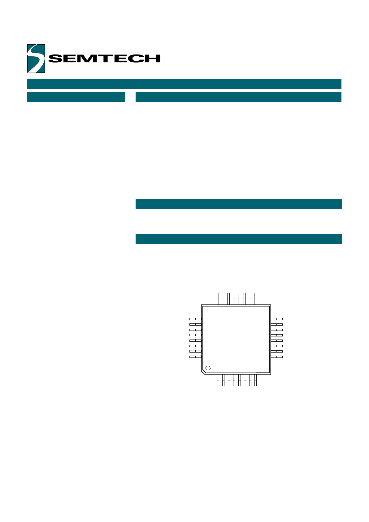
UR6HCPS2-SP40-FG
LQFP
CONF0
_CTS/_ATN
_PWR_OFF
SDATA
SCLK
TxD
RxD
E3DATA
OSCIN
_OSCOUT
VSS
LED3
LED2
LED1
LED0
RES0
CONF2
ASI/_SPI_SEL
X_PWR
VREF
_RESET
VSS2
VDD
_RTS/_SS
E0CLK
E0DATA
E1CLK
E1DATA
E2CLK
E2DATA
E3CLK
CONF1
• Typically consumes less than 1 µA
• Interfaces the host system via
either Asynchronous Serial
Interface or Serial Peripheral
Interface (SPI)
• Jumper selectable interface and
Baud rate
• Offers four PS/2 ports for the hotplug connection of external
keyboards or mice including
MouseWheel, 5 button mice and
absolute mode touch screens
• Easy to use, one way
communication protocol
• Operating voltage between 3
and 5 Volts
• Custom versions available in
small or large quantities
• Small 7x7 mm package to
accommodate slim designs
• H/PCs
• Web Phones
• PDAs
• System Legacy Support
The PS2AdaptTMis a Zero-Power
TM
protocol interpreter that can link an
AT/PS/2-compatible Human Input
Device (HID), such as a keyboard,
mouse, bar-code reader, etc. to any
host system equipped with either
Asynchronous Serial Interface (ASI)
or the Serial Peripheral Interface
(SPI).
The IC was designed specifically
for RISC-based portable devices
that are limited to ASI and SPI
interfaces. The PS2AdaptTMallows
designers to easily connect PS/2
devices to their system.
The UR6HCPS2-SP40 emulates all
the functions of the 8042 keyboard
controller which typically resides on
the AT/PS/2 motherboard. The
Zero-PowerTMPS2AdaptTMwill power
down even between
key presses and bewteen mouse
reports. Typical power
consumption is only 1 µA operating
between 3-5 Volts.
The UR6HCPS2-SP40 boasts 4
external PS/2 ports that support the
hot-plug connection of an external
PS/2 keyboard or mouse,
including MouseWheel, 5-button
mice and touch screens in absolute
mode.
Each of four external PS/2 ports
also support more than 140 key
scan codes including international
language keys, internet keys, and
power keys. The PS2AdaptTMalso
offers 4 reserved pins for LED
functions, their functions can be
customized by Semtech.
APPLICATIONS
PIN ASSIGNMENTS

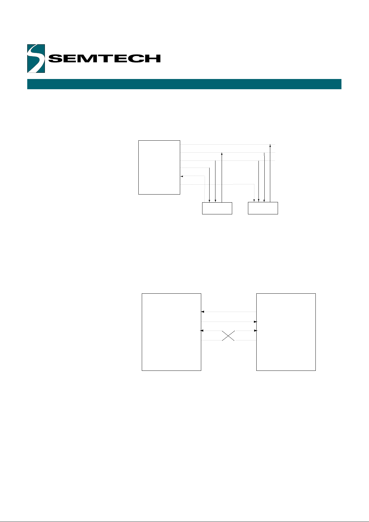
FUNCTIONAL DIAGRAM
ORDERING CODE
Copyright Semtech, 2002-2001
DOC6-PS2-SP40-DS-102
www.semtech.com
2
Package options
32-pin Plastic LQFP
Other materials
PS2AdaptTMEvaluation Kit
Pitch In mm’s
0.8 mm
Part number
EVK6-PS2-SP40-100
TA = -40°C to +85°C
UR6HCPS2-SP40-FG
Power
Management
Unit
Dual Mode
Serial
Communications
Port
External
PS/2 Port 3
External
PS/2 Port 2
External
PS/2 Port 1
SCLK
RxD
TxD
SS/RTS
ATN/CTS
PWR_OFF
E2CLK
E2DATA
E3CLK
E3DATA
E1CLK
E1DATA
External
PS/2 Port 0
HID Manager
SDATA
ASI/_SPI_SEL
E0CLK
E0DATA
PIN DEFINITIONS
Pin Numbers
Mnemonic LQFP Type Name and Function
Power Supply
VDD 8 PWR Positive Supply Voltage: +3V-+5V
VREF 5 AI Positive Analog Ref Voltage
VSS 11 PWR Ground: analog signal
VSS2 7 PWR Ground: negative supply voltage
_RESET 6 I Hardware Reset Pin:
at Low-level, this pin holds the
UR6HCPS2-SP40 in a reset state.
Oscillator Pins
OSCIN 9 I Oscillator input: connect ceramic
resonator with built-in load capacitors
or CMOS clock from external oscillator
4 MHz operating frequency
_OSCOUT 10 O Oscillator Output: connect ceramic
resonator with built-in load capacitors
or keep open if external oscillator
is used
PS/2 Ports
E0CLK 18 I/nD PS/2 Clock: for External Device 0
E0DATA 19 I/nD PS/2 Data: for Exter nal Device 0
E1CLK 20 I/nD PS/2 Clock: for External Device 1
E1DATA 21 I/nD PS/2 Data: for Exter nal Device 1
E2CLK 22 I/nD PS/2 Clock: for External Device 2
E2DATA 23 I/nD PS/2 Data: for Exter nal Device 2
E3CLK 24 I/nD PS/2 Clock: for External Device 3
E3DATA 25 I/nD PS/2 Data: for Exter nal Device 3
System Status
Monitoring
_PWR_OFF 30 I±Int Power Off Signal: capable of
Interrupt on both Positive and Negative
edges
X_PWR 4 AI External PS/2 Device Power
Detector
Communication
Interface
_SS/_RTS 17 I_Int Ready_To_Send: Active-Low
signal Input.Low-level indicates that
the Host System is ready to send
data from UR6HCPS2-SP40.
_ATN/_CTS 31 O Attention (SPI Mode) or
Clear_To_Send (Asynchronous
Serial Mode ): Active-Low signal
Output. Low-level indicates that the
UR6HCPS2-SP40 has data to send to
the Host System
TXD 27 O Transmit Data (Asynchronous
Serial Mode): Idle = "High" = 1
RXD 26 I Receive Data (Asynchronous
Serial Mode): Reserved future use
SDATA 29 Master-In-Slave-Out (SPI Mode):
keep open for ASI mode or tie to Gnd
SCLK 28 I Serial Clock (SPI Mode): in SPI
Mode, use the following Clock
sequence:Idle-high/ Negative-Edge
(Shift Data) \ Positive-Edge (Latch
Data), Idle-High. Keep open or tie to
Gnd for ASI mode
FUNCTIONAL DESCRIPTION
Copyright Semtech, 2002-2001
DOC6-PS2-SP40-DS-102
www.semtech.com
3
The PS2AdaptTMconsists
functionally of three major sections.
These are the Dual Mode Serial
Communications Interface, the
Power Management Unit, and the
HID Manager. All sections
communicate with each other and
operate concurrently.
HID MANAGER
OPERATIONS BELOW 5 V
The UR6HCPS2-SP40 Human Input
Device (HID) Manager is
responsible for the configuration
and handling of HID devices that
are attached to the controller
through the four external PS/2 ports.
The HID Manager has the following
responsibilities:
1. Initialize PS/2 keyboards and
mice
2. Mix the information from external
PS/2 devices
3. Formatting and relaying reports of
the HID devices to the Host.
The standard PS/2 devices are
specified for supply voltage of 5V.
Operations of the UR6PS2-SP40 at
a lower voltage (3V) are only
possible if the HID devices
connected to ALL external PS/2
ports are capable of 3V operations.

PIN DEFINITIONS, (CON’T)
Copyright Semtech, 2002-2001
DOC6-PS2-SP40-DS-102
www.semtech.com
4
Pin Numbers
Mnemonic LQFP Type Name and Function
Configuration Pins
CONF0 32 I Configuration pin 0; see Note 2
CONF1 1 I Configuration pin 1; see Note 2
CONF2 2 I Configuration pin 2; see Note 2
ASI/_SPI_SEL 3 I SPI/Serial Selector pin. High:Serial;
Reserved for
LED0 12 I/O Reserved LED Driver / GPIO
LED1 13 I/O Reserved LED Driver / GPIO
LED2 14 I/O Reserved LED Driver / GPIO
LED3 15 I/O Reserved LED Driver / GPIO
RES0 16 I/O Reserved GPIO
Note 1: An underscore in front of the pin mnemonic denotes an active low signal.
Note 2: When Asynchronous Serial Interface (ASI) mode is selected, ASI/_SPI_SEL pin is
high and pins CONF2:CONF1:CONF0 select the following Baud Rates:
111: 19200 bps; 110: 9600 bps; 101: 1200 bps; 100: 600 bps; 011: 300 bps
010: 31250 bps; 001: 62500 bps.
When SPI mode is selected, ASI/_SPI_SEL pin is low. If CONF0 is high, the trasnfer sequence
is MSB to LSB, otherwise, LSB to MSB.
Note 3: For ASI/_SPI_SEL pin use the following setting:
1: Asynchronous Serial Mode; 0: Serial Peripheral Interface (SPI) mode
Note 4: In ASI mode, SDATA and SCLK are driven to low after reset. In SPI mode, TXD, RXD,
CONF1 and CONF2 are driven to low after reset. In both ASI and SPI mode, LED0, LED1,
LED2, LED3 and RES0 are configured as inputs with pull-up resistors.
Pin Types Legend: AI=Analog Input; I=Input; O=Output; I/O=Input or Output;
I/nD=Input or Output with N-channel Open Drain driver;
Copyright Semtech, 2002-2001
DOC6-PS2-SP40-DS-102
www.semtech.com
5
COMMUNICATIONS INTERFACE FOR THE UR6HCPS2-SP40
The UR6HCPS2-SP40 offers two
modes of serial communications:
"Synchronous Peripheral Interface"
(SPI) mode and the "Asynchronous
Serial Interface" (ASI) mode.
The IC determines the mode of
communication with the Host during
power-up by reading the value of
the ASI/_SPI_SEL pin. If the pin is
tied high, the ASI mode is enabled.
If it is low, the SPI interface is
enabled.
The PS2AdaptTMimplements the SPI
mode by single direction
communication that supports bit
rates up to 250 Kb/s. Several Hosts
and companion chips implement
the SPI protocol in order to
communicate with a wide range of
peripherals such as EEPROMs, A/D
converters, MCUs and other system
components.
The UR6HCPS2-SP40 deploys the
_ATN as an additional hand-shake
signal in order to support low power
operation of the bus.
The PS2AdaptTMimplements the ASI
mode at fixed preselected baud
rates: 300bps, 600bps, 1200bps,
9600bps, 19200bps, 31250bps and
62500bps, depending on the
Configuration pins’ state on power
up.
In ASI mode, the UR6HCPS2-SP40
deploys the _RTS & _CTS as
additional hand-shake signals in
order to support low power
operation of the bus.
The diagrams below illustrate the SPI and ASI communications interfaces,
respectively.
SPI Communications Interface
Host
(master)
MOSI
MISO
SCLK
PS2Adapt
(slave)
Slave 2
TM
_SS1
_ATN
_SS2
SDATA
ASI Communications Interface
HOST
UR6HCPS2-SP40
_CTS
_CTS
_RTS _RTS
RxD
RxD
TxD
TxD
Copyright Semtech, 2002-2001
DOC6-PS2-SP40-DS-102
www.semtech.com
6
REPORTS
Overview
The PS2AdaptTMUR6HCPS2-SP40
will report three types of package
formats for relative mouse, absolute
mouse and keyboard report
respectively.
Each mouse packet contains 4
bytes; keyboard packet contains 2
bytes. The 7th bit of each byte is
used for synchronization. The 7th
bit for the first byte is 1 and for the
other bytes is 0.
Keyboard Data Report
8-bit key number (K0-K7) is an
identification of a keyboard key,
which is defined in the USAR key
table (see Page 7).
PS/2 Mouse Data Report
There are two different kinds of
mouse data packages for the
external PS/2 devices. One is
absolute mode that is for
touchscreens and the other is
relative mode for standard PS/2
devices, including MouseWheel.
The resolution for the absolute
mouse is 10 bits (1000 points) in X
and Y direction.
The relative mouse data format
takes into consideration the 5button and MouseWheel devices.
Keyboard Package Format
Bit Number
Byte # 76543210
1 1 1 Not Caps Num Scroll 1:Make K7
KBD Assigned Lock Lock Lock /0:Break
1:On 1:On 1:On
/0:Off /0:Off /0:Off
2 0 K6K5K4K3K2K1K0
Absolute Mode PS/2 Mouse Package Format
Bit Number
Byte # 76543210
1 10000000
Mouse Absolute 1 penup 1 penup 1 penup 1 penup 1 penup
2 0 Y9Y8Y7X* X9X8X7
3 0 X6X5X4X3X2X1X0
4 0 Y6Y5Y4Y3Y2Y1Y0
Note 4: The bits that are marked with X* are reserved for future use. Now the value given is
zero.
Relative Mode PS/2 Mouse Package Format
Bit Number
Byte # 76543210
1 1 0 1 Ysign Xsign M R L
Mouse Relative
2 0 X6X5X4X3X2X1X0
3 0 Y6Y5Y4Y3Y2Y1Y0
4 0 X* B5B4Z3Z2Z1Z0
Note 5: The bits that are marked with X* are reserved for future use. Now the value given is
zero.

Copyright Semtech, 2002-2001
DOC6-PS2-SP40-DS-102
www.semtech.com
7
PS/2 SCAN CODE SETS ACCORDING TO THE KEY NUMBER
Key Name Key PS/2 Set PS/2 Set PS/2 Set PS/2 Set
Number 1 Make 1 Break 2 Make 2 Break
No Event 0 None None None None
Overrun Error 1 FF None 0 None
POST Fail 2 FC None FC None
ErrorUndefined 3 UNASSIGNED UNASSIGNED UNASSIGNED UNASSIGNED
a A 4 1E 9E 1C F0 1C
b B 5 30 B0 32 F0 32
c C 6 2E AE 21 F0 21
d D 7 20 A0 23 F0 23
e E 8 12 92 24 F0 24
f F 9 21 A1 2B F0 2B
g G1022A234F0 34
h H1123A333F0 33
i I 12179743F0 43
j J 13 24 A4 3B F0 3B
k K 14 25 A5 42 F0 42
l L 15 26 A6 4B F0 4B
m M 16 32 B2 3A F0 3A
n N1731B131F0 31
o O18189844F0 44
p P1919994DF0 4D
q Q20109015F0 15
r R2113932DF0 2D
s S221F9F1BF0 1B
t T2314942CF0 2C
u U2416963CF0 3C
v V 25 2F AF 2A F0 2A
w W2611911DF0 1D
x X 27 2D AD 22 F0 22
y Y28159535F0 35
z Z 29 2C AC 1A F0 1A
1 ! 30 2 82 16 F0 16
2 @ 31 3 83 1E F0 1E
3 # 32 4 84 26 F0 26
4 $ 33 5 85 25 F0 25
5% 34 6 86 2E F0 2E
6 ^ 35 7 87 36 F0 36
7 & 36 8 88 3D F0 3D
8 * 37 9 89 3E F0 3E
9 ( 38 0A 8A 46 F0 46
0 ) 39 0B 8B 45 F0 45
Return 40 1C 9C 5A F0 5A
Escape 41 1 81 76 F0 76
Backspace 42 0E 8E 66 F0 66
Tab430F8F0DF0 0D
Space 44 39 B9 29 F0 29
-_ 45 0C 8C 4E F0 4E
= + 46 0D 8D 55 F0 55
[ { 47 1A 9A 54 F0 54
] } 481B9B5BF0 5B
\ | 49 2B AB 5D F0 5D
Europe 1 (Note 2) 50 2B AB 5D F0 5D
; : 51 27 A7 4C F0 4C
‘ “ 52 28 A8 52 F0 52
` ~ 53 29 A9 0E F0 0E

Copyright Semtech, 2002-2001
DOC6-PS2-SP40-DS-102
www.semtech.com
8
PS/2 SCAN CODE SETS ACCORDING TO THE KEY NUMBER
Key Name USAR Key PS/2 Set PS/2 Set PS/2 Set PS/2 Set
Number 1 Make 1 Break 2 Make 2 Break
, <5433B341F0 41
. >5534B449F0 49
/ ? 56 35 B5 4A F0 4A
Caps Lock 57 3A BA 58 F0 58
F1 58 3B BB 5 F0 05
F2 59 3C BC 6 F0 06
F3 60 3D BD 4 F0 04
F4 61 3E BE 0C F0 0C
F5 62 3F BF 3 F0 03
F6 63 40 C0 0B F0 0B
F7 64 41 C1 83 F0 83
F8 65 42 C2 0A F0 0A
F9 66 43 C3 1 F0 01
F10 67 44 C4 9 F0 09
F11 68 57 D7 78 F0 78
F12 69 58 D8 7 F0 07
Print Screen(Note 1)70 E0 37 E0 B7 E0 7C E0 F0 7C
Scroll Lock 71 46 C6 7E F0 7E
Pause 72 E1 1D 45 None E1 14 77 E1 None
E1 9D C5 F0 14 F0 77
Insert (Note 1) 73 E0 52 E0 D2 E0 70 E0 F0 70
Home (Note 1) 74 E0 47 E0 C7 E0 6C E0 F0 6C
Page Up (Note 1) 75 E0 49 E0 C9 E0 7D E0 F0 7D
Delete (Note 1) 76 E0 53 E0 D3 E0 71 E0 F0 71
End (Note 1) 77 E0 4F E0 CF E0 69 E0 F0 69
Page Down(Note 1)78 E0 51 E0 D1 E0 7A E0 F0 7A
Right Arrow (Note 1)79 E0 4D E0 CD E0 74 E0 F0 74
Left Arrow (Note 1) 80 E0 4B E0 CB E0 6B E0 F0 6B
Down Arrow(1) 81 E0 50 E0 D0 E0 72 E0 F0 72
Up Arrow (Note 1) 82 E0 48 E0 C8 E0 75 E0 F0 75
Num Lock 83 45 C5 77 F0 77
Keypad/(Note 1) 84 E0 35 E0 B5 E0 4A E0 F0 4A
Keypad * 85 37 B7 7C F0 7C
Keypad - 86 4A CA 7B F0 7B
Keypad + 87 4E CE 79 F0 79
Keypad Enter 88 E0 1C E0 9C E0 5A E0 F0 5A
Keypad 1 End 89 4F CF 69 F0 69
Keypad 2 Down 90 50 D0 72 F0 72
Keypad 3 PageDn 91 51 D1 7A F0 7A
Keypad 4 Left 92 4B CB 6B F0 6B
Keypad 5 93 4C CC 73 F0 73
Keypad 6 Right 94 4D CD 74 F0 74
Keypad 7 Home 95 47 C7 6C F0 6C
Keypad 8 Up 96 48 C8 75 F0 75
Keypad 9 PageUp 97 49 C9 7D F0 7D
Keypad 0 Insert 98 52 D2 70 F0 70
Keypad . Delete 99 53 D3 71 F0 71
Europe 2 (Note 2) 100 56 D6 61 F0 61
App 101 E0 5D E0 DD E0 2F E0 F0 2F
Keyboard Power 102 UNASSIGNED UNASSIGNED UNASSIGNED UNASSIGNED
Keypad = 103 59 D9 0F F0 0F
F13 104 5D DD 2F F0 2F
F14 105 5E DE 37 F0 37
F15 106 5F DF 3F F0 3F

Copyright Semtech, 2002-2001
DOC6-PS2-SP40-DS-102
www.semtech.com
9
PS/2 SCAN CODE SETS ACCORDING TO THE KEY NUMBER
Key Name USAR Key PS/2 Set PS/2 Set PS/2 Set PS/2 Set
Number 1 Make 1 Break 2 Make 2 Break
F16 107 UNASSIGNED UNASSIGNED UNASSIGNED UNASSIGNED
F17 108 UNASSIGNED UNASSIGNED UNASSIGNED UNASSIGNED
F18 109 UNASSIGNED UNASSIGNED UNASSIGNED UNASSIGNED
F19 110 UNASSIGNED UNASSIGNED UNASSIGNED UNASSIGNED
F20 111 UNASSIGNED UNASSIGNED UNASSIGNED UNASSIGNED
F21 112 UNASSIGNED UNASSIGNED UNASSIGNED UNASSIGNED
F22 113 UNASSIGNED UNASSIGNED UNASSIGNED UNASSIGNED
F23 114 UNASSIGNED UNASSIGNED UNASSIGNED UNASSIGNED
F24 115 UNASSIGNED UNASSIGNED UNASSIGNED UNASSIGNED
Keyboard Execute 116 UNASSIGNED UNASSIGNED UNASSIGNED UNASSIGNED
Keyboard Help 117 UNASSIGNED UNASSIGNED UNASSIGNED UNASSIGNED
Keyboard Menu 118 UNASSIGNED UNASSIGNED UNASSIGNED UNASSIGNED
Keyboard Select 119 UNASSIGNED UNASSIGNED UNASSIGNED UNASSIGNED
Keyboard Stop 120 UNASSIGNED UNASSIGNED UNASSIGNED UNASSIGNED
Keyboard Again 121 UNASSIGNED UNASSIGNED UNASSIGNED UNASSIGNED
Keyboard Undo 122 UNASSIGNED UNASSIGNED UNASSIGNED UNASSIGNED
Keyboard Cut 123 UNASSIGNED UNASSIGNED UNASSIGNED UNASSIGNED
Keyboard Copy 124 UNASSIGNED UNASSIGNED UNASSIGNED UNASSIGNED
Keyboard Paste 125 UNASSIGNED UNASSIGNED UNASSIGNED UNASSIGNED
Keyboard Find 126 UNASSIGNED UNASSIGNED UNASSIGNED UNASSIGNED
Keyboard Mute 127 UNASSIGNED UNASSIGNED UNASSIGNED UNASSIGNED
Keyboard Vol up 128 UNASSIGNED UNASSIGNED UNASSIGNED UNASSIGNED
Keyboard Vol Dn 129 UNASSIGNED UNASSIGNED UNASSIGNED UNASSIGNED
Keyboard Locking/ 130 UNASSIGNED UNASSIGNED UNASSIGNED UNASSIGNED
Caps Lock
Keyboard Locking 131 UNASSIGNED UNASSIGNED UNASSIGNED UNASSIGNED
Num Lock
Keyboard Locking 132 UNASSIGNED UNASSIGNED UNASSIGNED UNASSIGNED
Scroll Lock
Keyboard , 133 7E FE 6D F0 6D
(Brazilian Keypad .)
Keyboard Equal 134 UNASSIGNED UNASSIGNED UNASSIGNED UNASSIGNED
sign
Keyboard 135 73 F3 51 F0 51
Int'l 1 (Ro)
Keyboard Int’l 2 136 70 F0 13 F0 13
(Katakana/Hiragana)
Keyboard 137 7D FD 6A F0 6A
Int'l 3 ¥ (Yen)
Keyboard 138 79 F9 64 F0 64
Int'l 4 (Henkan)
Keyboard 139 7B FB 67 F0 67
Int'l 5 (Muhenkan)
Keyboard Int'l 6 140 5C DC 27 F0 27
(PC9800 Keypad , )
Keyboard Int'l 7 141 UNASSIGNED UNASSIGNED UNASSIGNED UNASSIGNED
Keyboard Int'l 8 142 UNASSIGNED UNASSIGNED UNASSIGNED UNASSIGNED
Keyboard Int'l 9 143 UNASSIGNED UNASSIGNED UNASSIGNED UNASSIGNED
Keyboard Lang 1 144 F2 None F2 None
(Hanguel/English)
Keyboard Lang 2 145 F1 None F1 None
(Hanja)
Keyboard Lang 3 146 78 F8 63 F0 63
(Katakana)

Copyright Semtech, 2002-2001
DOC6-PS2-SP40-DS-102
www.semtech.com
10
PS/2 SCAN CODE SETS ACCORDING TO THE KEY NUMBER
Key Name USAR Key PS/2 Set PS/2 Set PS/2 Set PS/2 Set
Number 1 Make 1 Break 2 Make 2 Break
Keyboard Lang 4 147 77 F7 62 F0 62
(Hiragana)
Keyboard Lang 5 148 76 F6 5F F0 5F
(Zenkaku/Hankaku)
Keyboard Lang 6 149 UNASSIGNED UNASSIGNED UNASSIGNED UNASSIGNED
Keyboard Lang 7 150 UNASSIGNED UNASSIGNED UNASSIGNED UNASSIGNED
Keyboard Lang 8 151 UNASSIGNED UNASSIGNED UNASSIGNED UNASSIGNED
Keyboard Lang 9 152 UNASSIGNED UNASSIGNED UNASSIGNED UNASSIGNED
Keyboard Alternate 153 UNASSIGNED UNASSIGNED UNASSIGNED UNASSIGNED
Erase
Keyboard SysReq/ 154 UNASSIGNED UNASSIGNED UNASSIGNED UNASSIGNED
Attention
Keyboard Cancel 155 UNASSIGNED UNASSIGNED UNASSIGNED UNASSIGNED
Keyboard Clear 156 UNASSIGNED UNASSIGNED UNASSIGNED UNASSIGNED
Keyboard Prior 157 UNASSIGNED UNASSIGNED UNASSIGNED UNASSIGNED
Keyboard Return 158 UNASSIGNED UNASSIGNED UNASSIGNED UNASSIGNED
Keyboard Separator159 UNASSIGNED UNASSIGNED UNASSIGNED UNASSIGNED
Keyboard Out 160 UNASSIGNED UNASSIGNED UNASSIGNED UNASSIGNED
Keyboard Oper 161 UNASSIGNED UNASSIGNED UNASSIGNED UNASSIGNED
Keyboard Clear 162 UNASSIGNED UNASSIGNED UNASSIGNED UNASSIGNED
/Again
Keyboard 163 UNASSIGNED UNASSIGNED UNASSIGNED UNASSIGNED
CrSel/Props
Keyboard ExSel 164 UNASSIGNED UNASSIGNED UNASSIGNED UNASSIGNED
Left Control 165 1D 9D 14 F0 14
Left Shift 166 2A AA 12 F0 12
Left Alt 167 38 B8 11 F0 11
Left GUI 168 E0 5B E0 DB E0 1F E0 F0 1F
Right Control 169 E0 1D E0 9D E0 14 E0 F0 14
Right Shift 170 36 B6 59 F0 59
Right Alt 171 E0 38 E0 B8 E0 11 E0 F0 11
Right GUI 172 E0 5C E0 DC E0 27 E0 F0 27
System Power 173 E0 5E E0 DE E0 37 E0 F0 37
System Sleep 174 E0 5F E0 DF E0 3F E0 F0 3F
System Wake 175 E0 63 E0 E3 E0 5E E0 F0 5E
Scan Next Track 176 E0 19 E0 99 E0 4D E0 F0 4D
Scan Previous Track177 E0 10 E0 90 E0 15 E0 F0 15
Stop 178 E0 24 E0 A4 E0 3B E0 F0 3B
Play/ Pause 179 E0 22 E0 A2 E0 34 E0 F0 34
Mute 180 E0 20 E0 A0 E0 23 E0 F0 23
Bass Boost 181 UNASSIGNED UNASSIGNED UNASSIGNED UNASSIGNED
Loudness 182 UNASSIGNED UNASSIGNED UNASSIGNED UNASSIGNED
Volume Up 183 E0 30 E0 B0 E0 32 E0 F0 32
Volume Down 184 E0 2E E0 AE E0 21 E0 F0 21
Bass Up 185 UNASSIGNED UNASSIGNED UNASSIGNED UNASSIGNED
Bass Down 186 UNASSIGNED UNASSIGNED UNASSIGNED UNASSIGNED
Treble Up 187 UNASSIGNED UNASSIGNED UNASSIGNED UNASSIGNED
Treble Down 188 UNASSIGNED UNASSIGNED UNASSIGNED UNASSIGNED
Media Select 189 6D E0 ED E0 50 E0 F0 50
Mail 190 E0 6C E0 EC E0 48 E0 F0 48
Calculator 191 E0 21 E0 A1 E0 2B E0 F0 2B

Copyright Semtech, 2002-2001
DOC6-PS2-SP40-DS-102
www.semtech.com
11
PS/2 SCAN CODE SETS ACCORDING TO THE KEY NUMBER
Key Name Key PS/2 Set PS/2 Set PS/2 Set PS/2 Set
Number 1 Make 1 Break 2 Make 2 Break
My Computer 192 E0 6B E0 EB E0 40 E0 F0 40
WWW Search 193 E0 65 E0 E5 E0 10 E0 F0 10
WWW Home 194 E0 32 E0 B2 E0 3A E0 F0 3A
WWW Back 195 E0 6A E0 EA E0 38 E0 F0 38
WWW Forward 196 E0 69 E0 E9 E0 30 E0 F0 30
WWW Stop 197 E0 68 E0 E8 E0 28 E0 F0 28
WWW Refresh 198 E0 67 E0 E7 E0 20 E0 F0 20
WWW Favorites 199 E0 66 E0 E6 E0 18 E0 F0 18
Note 1: In PS/2 mode, Scan Set 1 & 2, each keycode is preceded or followed by additional bytes of data. These
codes are documented in WHQLKEYS.DOC, available from Microsoft.
Note 2: These keys have various legends depending upon the locale for which the keyboard is manufactured.
Europe 1 is typically in AT-101 Key Position 42 next to the Enter key. Europe 2 is typically in AT-101 Key Position 45,
between the Left Shift and Z keys.

Copyright Semtech, 2002-2001
DOC6-PS2-SP40-DS-102
www.semtech.com
12
ASYNCHRONOUS SERIAL INTERFACE (ASI) MODE
Baud rate:
The PS2AdaptTMimplements the ASI mode at fixed preselected Baud rates: 300bps, 600bps, 1200bps, 9600bps,
19200bps, 31250bps and 62500bps, depending on the Configuration pins’ state on power up. The IC can achieve
these standard Baud rates by using a 4MHz oscillator.
Protocol:
In Serial mode, the PS2AdaptTMsupports transmission in one direction only (IC to Host). The IC starts the
transmission to the system when it has mouse/keyboard package pending. The data format is one start bit, 8 data
bits, no parity and one stop bit.
1. The UR6HCPS2-SP40 asserts _CTS low to indicate that a packet transfer will start.
2. The Host asserts _RTS low to indicate that it is ready to receive data.
_RTS low means that system can receive data (e.g. UART is operational).
3. The UR6HCPS2-SP40 places data on TXD line when it detects the _RTS low.
4. When one package is successfully transmitted, the IC raises _CTS.
Notes on the Protocol:
To assure fast transmission, the system must assert _RTS low as soon as possible. If the system is ready to receive
the data, it doesn't have to raise _RTS between packages.
The UR6HCPS2-SP40 checks _RTS after every byte transmission. If _RTS returns to high, it means that the
transmission was unsuccessful. The IC will raise _CTS to abort the transmission and the entire package will be retransmitted.
The maximum time of T1 is 10ms. If the system cannot assert _RTS low after 10ms of _CTS low, the IC will raise
_CTS to abort the transmission request. After that, the PS2AdaptTMwill try to start the transmission again.
1st
Byte
Last
Byte
t1
_CTS
TXD
_RTS
Figure 1: Serial Transmission Timing

Copyright Semtech, 2002-2001
DOC6-PS2-SP40-DS-102
www.semtech.com
13
SERIAL PERIPHERAL INTERFACE (SPI) MODE
The Serial Peripheral Interface (SPI) is a synchronous bi-directional multi-slave protocol. In SPI mode, the
PS2Adapt
TM
acts as a slave device. The IC only supports transmission and doesn't support receiving. SPI data
transfer can be performed at a maximum clock rate of 500 KHz. If CONF0 pin is high, the data transfer sequence is
MSB to LSB; if CONF0 pin is low the sequence is LSB to MSB. The SDATA pin outputs data every time the transfer
clock changes from high to low level.
Protocol:
1. The UR6HCPS2-SP40 asserts _ATN low to indicate that a mouse packet is waiting for transfer.
2. The Host asserts _SS low to indicate that it is ready to receive data. _SS low means the system selected SPI
PS2AdaptTMas its communication device.
3. On detecting _SS low, the IC enables the SPI interface and places data in the SPI data TX buffer. After a short
delay, the system supplies eight clocks to get the data from the IC. The minimum time t2 from _SS low to first SPI
clock is 50us.
4. When a byte is transferred successfully, the system has to wait a minimum of 50us to begin the clocks for next
byte transmission.
5. When the four-byte mouse package / 2-byte keyboard package is transmitted, the system stops the SPI clock. If
it needs to communicate with other SPI devices, it has to wait for _ATN return to high. _ATN high means the SPI port
of UR6HCPS2-SP40 is now in high Impedance State.
Figure 2: SPI Transmission Timing: (_SS toggles for every package).
Notes on the Protocol:
To assure the fast transmission, system must assert _SS low as soon as possible, see Figure 2. If the system is
ready to get data, it doesn't have to raise _SS between packages, see Figure 3.
_ATN
_SS
SDATA
1st
Byte
Last
Byte
t1 t2
SCLK
2nd
Byte
t3
t4

Copyright Semtech, 2002-2001
DOC6-PS2-SP40-DS-102
www.semtech.com
14
PROTOCOLS FOR THE UR6HCPS2-SP 40 IN SPI MODE (CON’T)
SPI Communication Timing Parameters
Symbol Description Min Max Units
t1 _ATN low to _SS low 10 ms
t2 _SS low to first clock 50 5000 us
(_SS toggles for every package)
t2’ _ATN low to first clock 50 5000 us
(_SS low)
t3 Last clock of transmitted 50 5000 us
byte to next byte’s first clock
t4 Last byte TX finish to 30 us
_ATN to high
_ATN
_SS
SDATA
1st
Byte
Last
Byte
SCLK
2nd
Byte
t3
t4
t2
Figure 3: SPI Packet Transmission Timing: (_SS low always).

POWER MANAGEMENT
Copyright Semtech, 2002-2001
DOC6-PS2-SP40-DS-102
www.semtech.com
15
Modes of Operation
The UR6HCPS2-SP40 has two
modes of operation relating to its
power consumption.
The "Stop" mode is the lowest
power consumption mode. In this
mode, the oscillator is stopped and
the IC consumes only 1 µA of
leakage current. This is the default
mode to which the IC will revert to
when it is idle.
The "Run" mode is entered briefly,
only to process an event or while an
interrupt-generating signal condition
persists. The IC will remain in this
mode until there are no tasks to
handle, such as PS/2 reports or
inititalization of PS/2 devices.
The PS/2 devices connected to the
four external PS/2 ports are
initialized at different sampling
rates, depending on the port: PS/2
port 0 and PS/2 port 1 to 100
packages per second and 40
packages per second for PS/2 port
3 and PS/2 port 4. When mice
plugged into PS/2 port 0 and 1 are
moved, the PS2AdaptTMwill typically
stay in stop mode for 25% of the
working time. When mice plugged
into PS/2 port 3 and 4 are moved
with a slower sampling rate, the
PS2Adapt
TM
will typically stay in stop
mode for 72% of working time.
Therefore, we recommend that PS/2
port 3 and 4 are used for mice, if
there is no specific requirement of
mice sampling rate.
Note 1: When there is no mouse motion, all
ports have same power consumption, less
than 1µA.
Note 2: When a keyboard is plugged into
these ports, the rate of the power saving are
same, less than 1µA.
The PS2AdaptTMimplements two power management methods: systemcoordinated power management and Self Power ManagementTM(SPM).
System-coordinated power management is implemented by the _PWR_OFF
pin (Power Off). If the _PWR_OFF pin is low, the PS2Adapt™ will disable all
external PS/2 device reports to save power and to turn off keyboard Leds.
Self-Power ManagementTMis a method implemented by the PS2AdaptTMIC
that, independently of any system intervention, results in the lowest power
consumption possible within the given parameters of its operation. Through
Self Power ManagementTM, the PS2AdaptTMIC is capable of typically
operating at only 1 µA, independent of the state of the system. Self Power
ManagementTMprimarily determines the actual power consumption of the
IC.
Even when the Host is in the active state, the IC can still operate most of
the time at only 1 µA, even with active external PS/2 devices attached to it.
Run
Stop
PWR_OFF Pin High
AND
External PS/2 Report
PWR_OFF Pin Low
OR
No Task
Copyright Semtech, 2000-2001
DOC6-PS2-SP40-DS-102
www.semtech.com
16
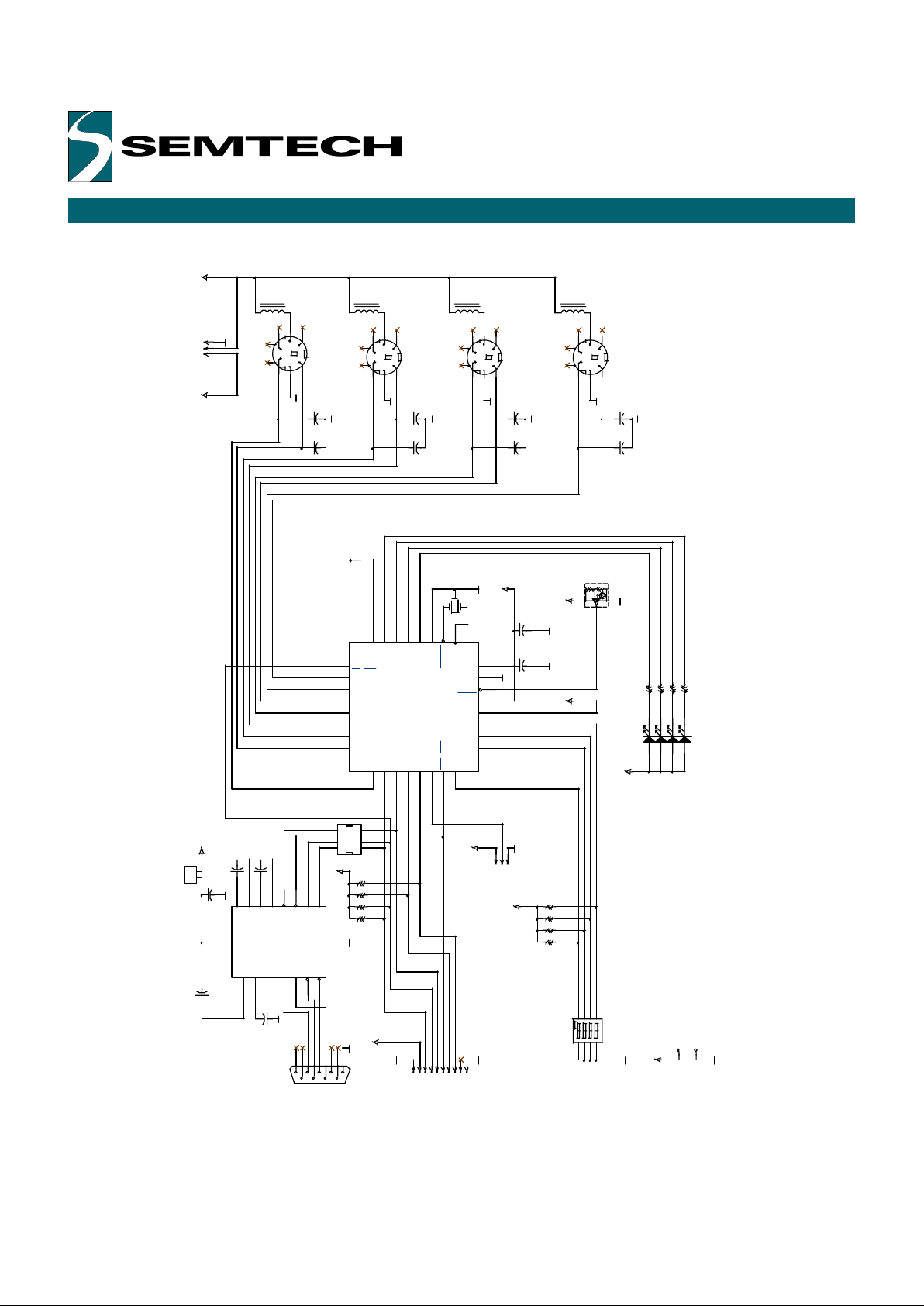
EVALUATION BOARD SCHEMATIC FOR THE UR6HCPS2-SP40-FG
RTS
RTS
SDATA
UR6HCPS2-SP40-FG Rev 1.0
CTS
TXD
RXD
TXD
SCLK
RXD
CTS
(C)2000 USAR, A Semtech Company
_CTS / _AT N
E3DATA
SDATA
CONF2
LED2
RXD
E2DATA
E3CLK
RES0
TXD
_RTS / _SS
SCLK
PWR_OFF
LED1
_RESET
E0DATA
LED3
E1DATA
LED0
CONF1
E1CLK
CONF0
E1CLK
E0CLK
SCISPI_SEL
VCC
GND
GND
GND
GND
GND
GND
VCC
GND
GND
GND
GND
X_PWR
GND
GND
VCC
VCC
GND
GND
GND
GND
GND
GND
VCC
GND
VCC
VCC
GNDGND
GND
VCC
VCC
X_PWR
VCC
GND
+
C2
10uF
RN1
330
135
78
642
C4
47pF
RN2
10K
1
3
5
7 8
6
4
2
L4
12uH
C7
47pF
JP6
CON_SIP3
123
+
C14
1uF
C10
47pF
L3
12uH
JP7
CON2
1
2
JP4
MDIN6_SH
642
531
7
8
+
C15
1uF
RN3
10K
1
3
5
7 8
6
4
2
P1
CON_DB9
594837261
D4
JP5
CON_SIP3
1
2
3
L1
12uH
C5
47pF
+
C11
1uF
S1
SW_DIP_4
123
4
876
5
+
C13
10uF
U1
UR6HCPS2-SP40-FG
32-PIN LQFP
1
2
3
4
5
6
7
8
9101112131415
16
17
18
19
20
21
22
23
24
25262728293031
32
CONF1
CONF2
ASI/_SPI_SEL
X_PWR
VREF
RESET
VSS2
VDD
OSCIN
OSCOUT
VSS
LED3
LED2
LED1
LED0
RES0
RTS / SS
E0CLK
E0DATA
E1CLK
E1DATA
E2CLK
E2DATA
E3CLK
E3DATA
RXD
TXD
SCLK
SDATA
PWR_OFF
CTS / ATN
CONF0
C8
47pF
U3
MAX232
1345111012
9
2
6
14713
8
1615
C1+
C1-
C2+
C2-
T1IN
T2IN
R1OUT
R2OUT
V+
V-
T1OUT
T2OUT
R1IN
R2IN
VCCGND
D1
JP3
MDIN6_SH
642
531
7
8
RES0
L2
12uH
D2
JP1
MDIN6_SH
642
531
7
8
JP2
MDIN6_SH
642
531
7
8
C3
47pF
C6
47pF
+
C12
1uF
JP9
1
2
3
4
5
6
7
8
1
2
3
4
5
6
7
8
JP8
CON_1X10
123456789
10
C9
47pF
Y1
4.00MHz
D3
VCC
GND
U2
TC54VC2702ECB
1
23
C1
.1uF
Copyright Semtech, 2000-2001
DOC6-PS2-SP40-DS-102
www.semtech.com
17
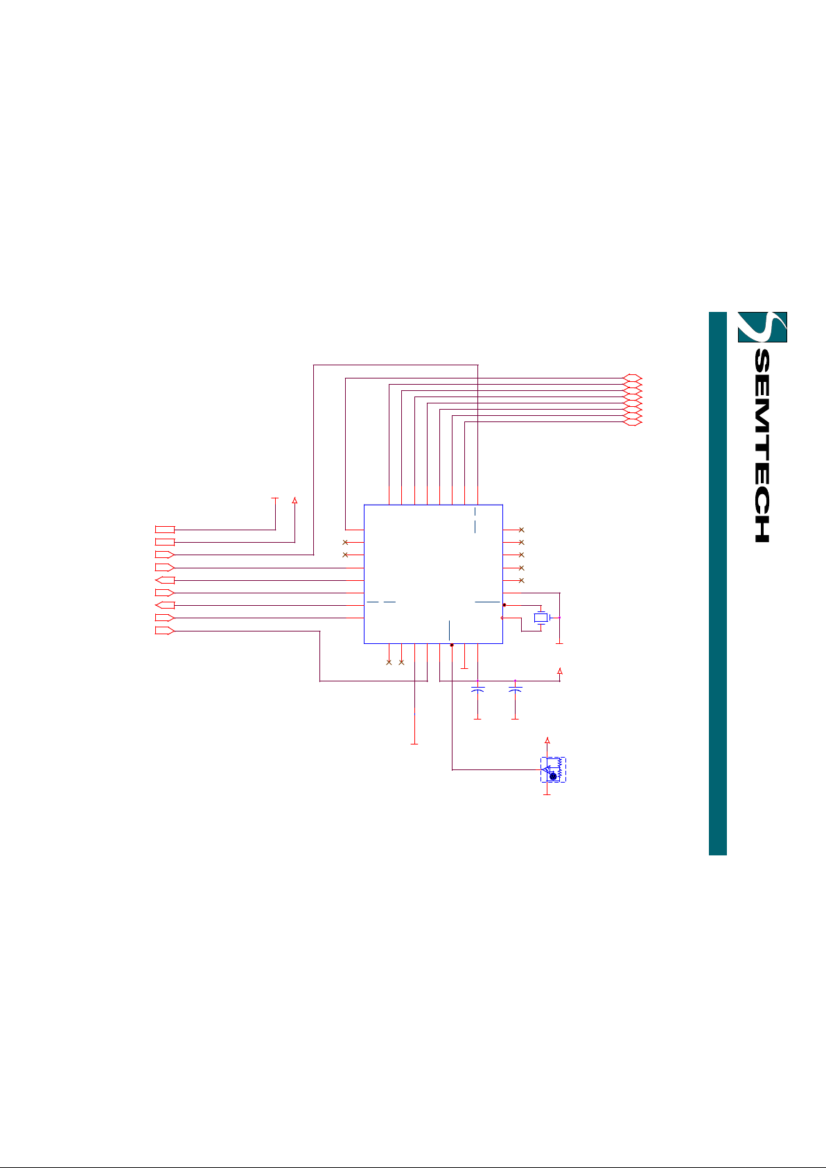
SUGGESTED SCHEMATIC FOR THE UR6HCPS2-SP40-FG IN SPI MODE
Revision 1.0UR6HCPS2-SP40-FG-SPI.SCH
PS/2 to Serial Adapter UR6HCPS2-SP40-FG ( SPI Interface)
(C)2000 USAR, A Semtech Company
NOTES:
CONF0 High: MSB first; Low: LSB first
PWR_OFF High: Power On; Low: Power Off
E3DATA
E2DATA
E3CLK
_RTS / _SS
SCLK
PWR_OFF
_RESET
SDATA
E0DATA
E1DATA
E1CLK
E1CLK
E0CLK
_CTS / _ATN
VCC
GND
GND
VCC
GND
GND
GND
GND
VCC
GND
+
C2
10uF
Y1
4.00MHz
R1
10K
U2
TC54VC2702ECB
1
23
C1
.1uF
U1
UR6HCPS2-SP40-FG
32-PIN LQFP
1234567
8
9
10
11
12
13
14
15
16
17
18
19
20
21
22
23
24
25
26
27
28
29
30
31
32
CONF1
CONF2
ASI/_SPI_SEL
X_PWR
VREF
RESET
VSS2
VDD
OSCIN
OSCOUT
VSS
LED3
LED2
LED1
LED0
RES0
RTS / SS
E0CLK
E0DATA
E1CLK
E1DATA
E2CLK
E2DATA
E3CLK
E3DATA
RXD
TXD
SCLK
SDATA
_PWR_OFF
CTS / ATN
CONF0
_ATN
MISO
E3DATA
E3CLK
E2DATA
E2CLK
E1DATA
E1CLK
E0DATA
E0CLK
X_PWR
CONF0
PWR_OFF
SCLK
_SS
VCC
GND
Copyright Semtech, 2000-2001
DOC6-PS2-SP40-DS-102
www.semtech.com
18
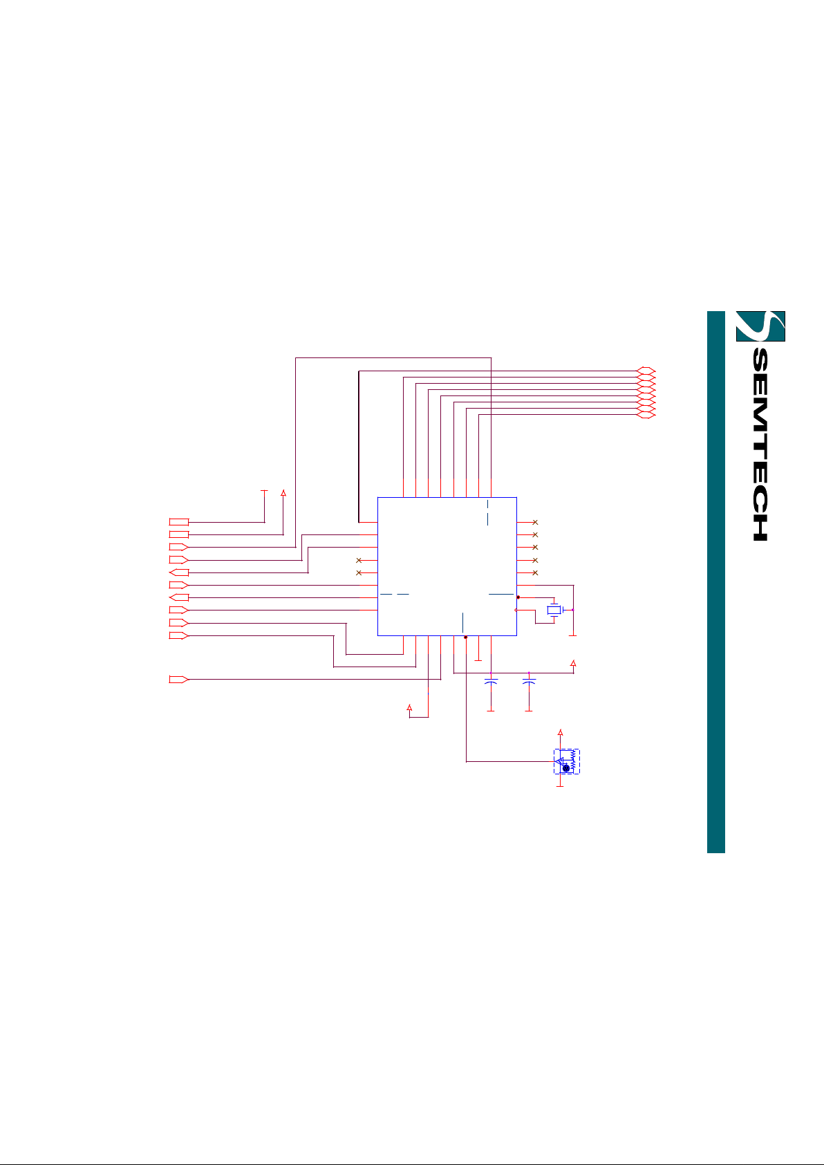
SUGGESTED SCHEMATIC FOR THE UR6HCPS2-SP40-FG IN SERIAL MODE
Revision 1.0UR6HCPS2-SP40-FG-SCI.SCH
PS/2 to Serial Adapter UR6HCPS2-SP40-FG ( Serial Interface)
(C)2000 USAR SYSTEMS, A Semtech Company
NOTES:
PWR_OFF High: Power On;Low: Power Off
CONF2 CONF1 CONF0
111: 19200 bps
110: 9600 bps
101: 1200 bps
100: 600 bps
011: 300 bps
010: 31250 bps
001: 62500 bps
E3DATA
E2DATA
E3CLK
_RTS / _SS
PWR_OFF
_RESET
E0DATA
E1DATA
E1CLK
E1CLK
E0CLK
_CTS / _ATN
VCC
GND
GND
VCC
GND
GND
GND
GND
VCC
VCC
+
C2
10uF
Y1
4.00MHz
U2
TC54VC2702ECB
1
23
C1
.1uF
U1
UR6HCPS2-SP40-FG
32-PIN LQFP
1234567
8
9
10
11
12
13
14
15
16
17
18
19
20
21
22
23
24
25
26
27
28
29
30
31
32
CONF1
CONF2
ASI/_SPI_SEL
X_PWR
VREF
RESET
VSS2
VDD
OSCIN
OSCOUT
VSS
LED3
LED2
LED1
LED0
RES0
RTS / SS
E0CLK
E0DATA
E1CLK
E1DATA
E2CLK
E2DATA
E3CLK
E3DATA
RXD
TXD
SCLK
SDATA
_PWR_OFF
CTS / ATN
CONF0
_CTS
TXD
E3DATA
E3CLK
E2DATA
E2CLK
E1DATA
E1CLK
E0DATA
E0CLK
X_PWR
_RTS
RXD
PWR_OFF
CONF0
CONF1
CONF2
GND
VCC
Copyright Semtech, 2000-2001
DOC6-PS2-SP40-DS-102
www.semtech.com
19
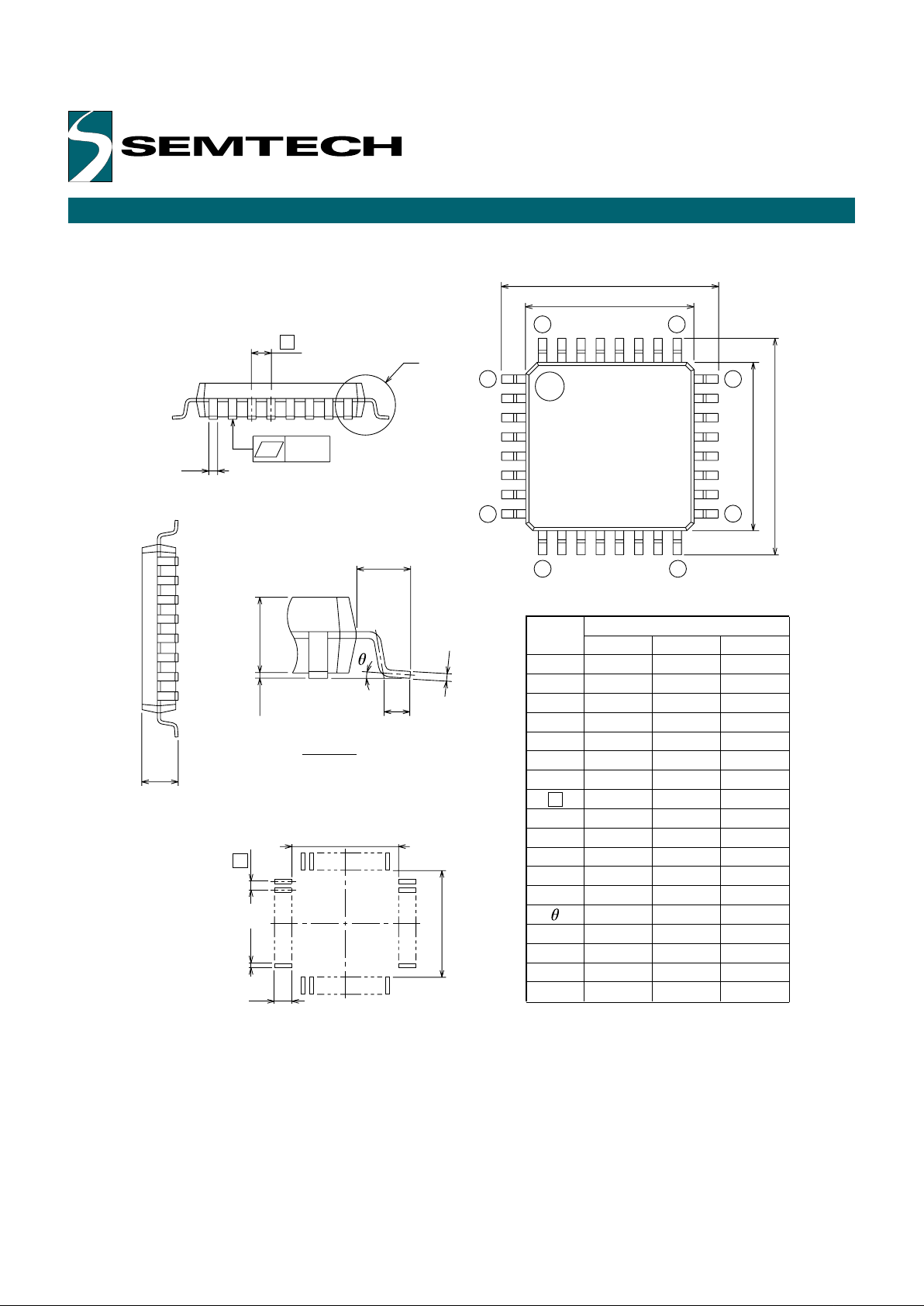
MECHANICAL INFORMATION FOR FG (32-PIN LQFP) PACKAGE
A
e
F
b
y
c
A1 A2
L1
L
Detail F
e
M
D
ME
b2
I2
Recommended PCB Footprint
–
0.1
–
––
0.2
–
–
––
–
–
––
–
Symbol
Min Nom Max
A
A
2
b
c
D
E
H
E
L
L
1
y
b
2
Dimension in Millimeters
H
D
A1
0.5
––
I
2
1.0
––
M
D
7.4
––
M
E
7.4
10ϒ0ϒ
0.1
1.0
0.70.50.3
9.29.08.8
9.29.08.8
0.8
7.17.06.9
7.17.06.9
0.1750.1250.105
0.450.350.3
1.4
0
1.7
e
E
H
E
1
8
9
32 25
24
16
17
HD
D
Copyright Semtech, 2000-2001
DOC6-PS2-SP40-DS-102
www.semtech.com
20
ELECTRICAL SPECIFICATIONS
Absolute Maximum Ratings
Ratings Symbol Value Unit
Supply Voltage Vdd -0.3 to 7.0 V
Input Voltage Vin Vss -0.3 to Vdd +0.3 V
Current Drain per Pin I 20 mA
(not including Vss or Vdd)
Operating Temperature Ta T low to T high
UR6HCSP2-SP40 -20 to +85 ° C
Storage Temperature Range Tstg -40 to +125 ° C
DC Electrical Characteristics, Temperature range=T low to T high unless otherwise noted)
Characteristic Symbol Min Typ Max Unit
Supply Voltage 3.0 5.0 5.5 V
Output Voltage (10 µA load) Voh Vdd–0.1 V
Vol 0.1
Input High Voltage Vih 0.8 x Vdd Vdd V
Input Low Voltage Vil Vss 0.2xVdd V
Input Current Iin +/- 1 µA
Supply Current
(Vdd=5.0 Vdc+/-10%, Vss=0) Idd 3.0 TBD mA
Control Timing (Vdd=5.0 Vdc +/-10%, Vss=0 Vdc, Temperature range=T low to T high unless otherwise noted)
Characteristic Symbol Min Typ Max Unit
Frequency of Operation fosc MHz
Resonator Option 4.0
External Clock Option 4.0

Copyright Semtech, 2000-2001
DOC6-PS2-SP40-DS-102
www.semtech.com
21
This Page Left Intentionally Blank

Copyright Semtech
DOC6-PS2-SP40-DS-102
www.semtech.com
22
For sales information
and product literature,
contact:
HID & System Mgmt Division
Semtech Corporation
568 Broadway
New York, NY 10012
hidinfo@semtech.com
http://www.semtech.com
212 226 2042 Telephone
212 226 3215 Telefax
Semtech Western Regional Sales
805-498-2111 Telephone
805-498-3804 Telefax
Semtech Central Regional Sales
972-437-0380 Telephone
972-437-0381 Telefax
Semtech Eastern Regional Sales
203-964-1766 Telephone
203-964-1755 Telefax
Semtech Asia-Pacific Sales Office
+886-2-2748-3380 Telephone
+886-2-2748-3390 Telefax
Semtech Japan Sales Office
+81-45-948-5925 Telephone
+81-45-948-5930 Telefax
Semtech Korea Sales Sales
+82-2-527-4377 Telephone
+82-2-527-4376 Telefax
Northern European Sales Office
+44 (0)2380-769008 Telephone
+44 (0)2380-768612 Telefax
Southern European Sales Office
+33 (0)1 69-28-22-00 Telephone
+33 (0)1 69-28-12-98 Telefax
Central European Sales Office
+49 (0)8161 140 123 Telephone
+49 (0)8161 140 124 Telefax
Copyright 2000-2001 Semtech Corporation. All rights reserved.
PS2Adapt and Zero-Power are trademarks of Semtech Corporation.
Semtech is a registered trademark of Semtech Company. All other
trademarks belong to their respective companies.
INTELLECTUAL PROPERTY DISCLAIMER
This specification is provided "as is" with no warranties whatsoever
including any warranty of merchantability, fitness for any particular
purpose, or any warranty otherwise arising out of any proposal,
specification or sample. A license is hereby granted to reproduce
and distribute this specification for internal use only. No other
license, expressed or implied to any other intellectual property
rights is granted or intended hereby. Authors of this specification
disclaim any liability, including liability for infringement of proprietary
rights, relating to the implementation of information in this
specification. Authors of this specification also do not warrant or
represent that such implementation(s) will not infringe such rights.
 Loading...