


SX8724
ZoomingADC™ for Pressure and Temperature Sensing
ADVANCED COMMUNICATIONS & SENSING
Description
The SX8724 is a data acquisition system based on
Semtech’s low power ZoomingADC™ technology. It
directly connects most types of miniature sensors
with a general purpose microcontroller.
With 3 differential inputs, it can adapt to multiple
sensor systems. Its digital outputs are used to bias
or reset the sensing elements.
Applications
• Industrial pressure sensing
• Industrial temperature sensing
• Barometer
• Compass
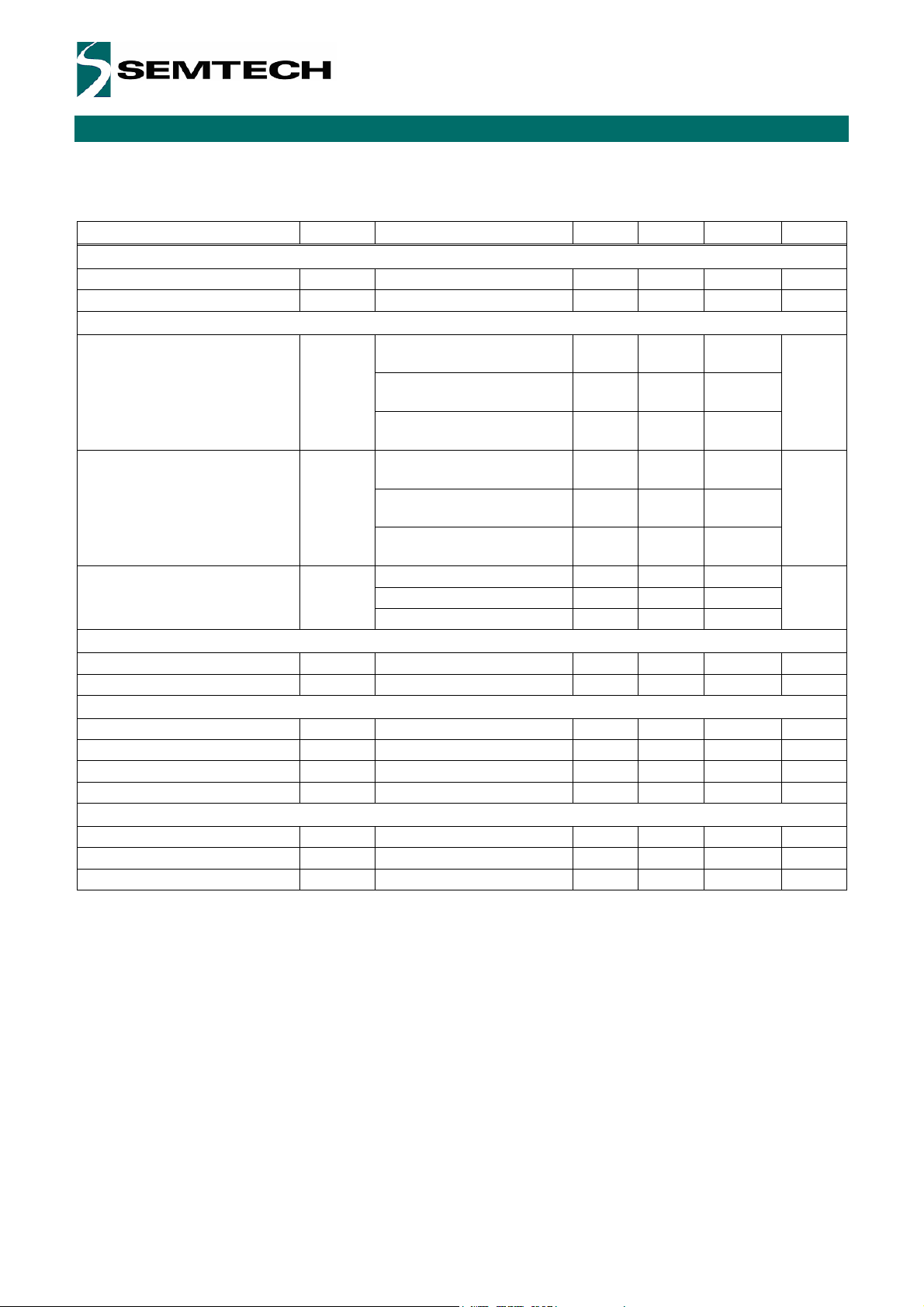
Functional Block Diagram
Features
• Up to 16-bit differential data acquisition
• Programmable gain: (1/12 to 1000)
• Sensor offset compensation up to 15 times
full scale of input signal
• 3 differential or 6 single-ended signal inputs
• Programmable Resolution versus Speed
versus Supply current
• 4 digital outputs to bias Sensors
• Internal or external voltage reference
• Internal time base
• Low-power (250 uA for 16b @ 500 S/s)
• 2-wire interface
Ordering Information
Device Package Reel quantity
SX8724E082TRT
SX8724E082TDT
1) Available in tape and reel only
2) Lead free, WEEE and RoHS compliant.
MLPQ-16 4x4
MLPQ-16 4x4
3000
1000
REF MUX
SIGNAL MUX
V1.23 © 2009 Semtech Corp. www.semtech.com
1

SX8724
ZoomingADC™ for Pressure and Temperature Sensing
ADVANCED COMMUNICATIONS & SENSING
Table of Contents
Description..............................................................................................................................................................1
Applications............................................................................................................................................................1
Features ..................................................................................................................................................................1
Ordering Information .............................................................................................................................................1
Functional Block Diagram.....................................................................................................................................1
Absolute Maximum Ratings..................................................................................................................................4
Electrical Characteristics ......................................................................................................................................5
ZoomingADC Specifications.................................................................................................................................6
Timing Characteristics ..........................................................................................................................................8
2-WIRE Timing Waveforms ...................................................................................................................................8
Pin Configuration ...................................................................................................................................................9
Marking Information...............................................................................................................................................9
Pin Description.......................................................................................................................................................9
Circuit Description ...............................................................................................................................................10
General Description ..............................................................................................................................................10
Block Diagram.......................................................................................................................................................10
VREF..................................................................................................................................................................... 10
GPIO ..................................................................................................................................................................... 11
Charge Pump........................................................................................................................................................ 12
RC Oscillator......................................................................................................................................................... 13
2-WIRE.................................................................................................................................................................. 14
2-WIRE Communication Format........................................................................................................................... 14
2-WIRE Address....................................................................................................................................................14
ZoomingADC ........................................................................................................................................................15
Features ................................................................................................................................................................ 15
Overview ............................................................................................................................................................... 15
ZADC Description..................................................................................................................................................15
Acquisition Chain...................................................................................................................................................15
Registers ............................................................................................................................................................... 17
ZADC Detailed Functionality Description..............................................................................................................18
Continuous-Time vs. On-Request.........................................................................................................................18
Input Multiplexers.................................................................................................................................................. 19
Programmable Gain Amplifiers .............................................................................................................................20
PGA & ADC Enabling............................................................................................................................................ 21
PGA1..................................................................................................................................................................... 21
PGA2..................................................................................................................................................................... 21
PGA3..................................................................................................................................................................... 21
ADC Characteristics..............................................................................................................................................22
Conversion Sequence...........................................................................................................................................22
Over-Sampling Frequency ....................................................................................................................................22
Over-Sampling Ratio.............................................................................................................................................23
Elementary Conversions....................................................................................................................................... 23
Resolution ............................................................................................................................................................. 24
Conversion Time and Throughput......................................................................................................................... 25
Output Code Format .............................................................................................................................................26
Power Saving Modes ............................................................................................................................................27
Registers Map....................................................................................................................................................... 28
Registers Descriptions ..........................................................................................................................................28
RC Register........................................................................................................................................................... 28
GPIO Registers..................................................................................................................................................... 29
ZADC Registers .................................................................................................................................................... 30
Mode Register.......................................................................................................................................................31
Optional Operating Modes: External Voltage Reference Option .......................................................................... 32
Application Hints..................................................................................................................................................33
Recommended Operation Mode and Registers Settings......................................................................................33
Operation Mode..................................................................................................................................................... 33
V1.23 © 2009 Semtech Corp. www.semtech.com
2

SX8724
ZoomingADC™ for Pressure and Temperature Sensing
ADVANCED COMMUNICATIONS & SENSING
Registers Settings................................................................................................................................................. 33
Schematic.............................................................................................................................................................. 34
Input Impedance.................................................................................................................................................... 35
Switched Capacitor Principle ................................................................................................................................36
PGA Settling or Input Channel Modifications........................................................................................................37
PGA Gain & Offset, Linearity and Noise............................................................................................................... 37
Frequency Response............................................................................................................................................ 38
Power Reduction...................................................................................................................................................39
Recommended Design for Other 2-WIRE Devices Connection ...........................................................................39
Typical Performance............................................................................................................................................40
Linearity................................................................................................................................................................. 40
Integral Non-Linearity............................................................................................................................................40
Differential Non-Linearity....................................................................................................................................... 43
Noise ..................................................................................................................................................................... 44
Gain Error and Offset Error................................................................................................................................... 46
Power Consumption..............................................................................................................................................47
PCB Layout Considerations................................................................................................................................49
How to Evaluate....................................................................................................................................................49
Package Outline Drawing: MLPQ-16 4x4...........................................................................................................50
Land Pattern Drawing: MLPQ-16 4x4.................................................................................................................51
Tape and Reel Specification ...............................................................................................................................52
V1.23 © 2009 Semtech Corp. www.semtech.com
3

SX8724
ZoomingADC™ for Pressure and Temperature Sensing
ADVANCED COMMUNICATIONS & SENSING
Absolute Maximum Ratings
Exceeding the specifications below may result in permanent damage to the device or device malfunction.
Operation outside the parameters specified in the Electrical Characteristics section is not implied.
Parameter Symbol Comments / Conditions Min Max Unit
Power supply V
Storage temperature T
Temperature under bias T
Input voltage VSS - 300 V
Peak reflow temperature T
Notes: This device is ESD sensitive. Use of standard ESD handling precautions is required.
VSS - 0.3 5.7 V
BATT
-55 150 °C
STORE
-40 140 °C
BIAS
V
Max sensor common mode
VR_P
V
VR_N
260 °C
PKG
VSS - 300 V
+300 mV
BATT
+300 mV
BATT
V1.23 © 2009 Semtech Corp. www.semtech.com
4
SX8724
ZoomingADC™ for Pressure and Temperature Sensing
ADVANCED COMMUNICATIONS & SENSING
Electrical Characteristics
All values are valid within the operating conditions unless otherwise specified.
Parameter Symbol Comments / Conditions Min Typ Max Unit
Operating conditions
Power supply V
Operating temperature TOP -40 125 ° C
Current consumption
Active current, @ 30 °C, 5.5 V IOP
Active current, @ 30 °C, 3.3 V IOP
Sleep current I
Time base
Max ADC over-sampling frequency F
Min ADC over-sampling frequency F
Digital I/O
Input logic high VIH 0.7 V
Input logic low VIL 0.3 V
Output logic high VOH I
Output logic low VOL I
VREF: Internal Bandgap Reference
Absolute output voltage V
Variation over Temperature V
Total Output Noise V
2.4 5.5 V
BATT
16 b @ 250 Sample/s
ADC, fs = 125 kHz
16 b @ 1 kSample/s
PGA3 + ADC, fs= 500 kHz
16 b + gain 1000 @ 1 kSample/s
PGA3,2,1 + ADC, fs = 500kHz
16 b @ 250 Sample/s
PGA3 + ADC, fs = 125 kHz
16 b @ 1 kSample/s
PGA3 + ADC, fs= 500 kHz
16 b + gain 1000 @ 1 kSample/s
PGA3,2,1 + ADC, fs = 500kHz
sleep
@ 25 °C 450 500 550 kHz
Smax
@ 25 °C 56.25 62.5 68.75 kHz
Smin
@ 30 °C 75 200
up to 85 °C 100
@125 °C 150
< 4mA V
OH
< 4mA 0.4 V
OL
> 3V 1.19 1.22 1.25 V
BATT
> 3V, ref to 25° C -1 +1 %
BATT
> 3V, rms, broadband 1 mV
BATT
250 300
700 800
1000 1200
150
300
850
-0.4 V
BATT
µA
µA
nA
BATT
BATT
V1.23 © 2009 Semtech Corp. www.semtech.com
5

SX8724
ZoomingADC™ for Pressure and Temperature Sensing
ADVANCED COMMUNICATIONS & SENSING
ZoomingADC Specifications
Unless otherwise specified: Temperature TA = +25° C, VDD = +5V, GND = 0V, V
fS = 250 kHz, PGA3 on with Gain = 1, PGA1&PGA2 off, offsets GDOff2 = GDOff3 = 0. Power operation: normal (IB_AMP_ADC[1:0] =
IB_AMP_PGA[1:0] = '01'). For resolution n = 12 bits: OSR = 32 and N
Bandgap chopped at N
Parameter Symbol Comments / Conditions Min Typ Max Unit
Analog Input
Differential Input Voltage Ranges
VIN = (V
INP
Reference Voltage Range
V
= (V
REF, ADC
Programmable Gain Amplifier (PGA)
Total PGA Gain GD
PGA1 Gain GD1 See Table 5 1 10 V/V
PGA2 Gain GD2 See Table 6 1 10 V/V
PGA3 Gain GD3 Step = 1/12 V/V, See Table 8 0 127/12 V/V
Gain Setting Precision (each stage) -3
Gain Temperature Dependence
PGA2 Offset GDoff2 Step = 0.2 V/V, See Table 7 -1 1 V/V
PGA3 Offset GDoff3 Step = 1/12 V/V, See Table 9 -63/12 63/12 V/V
Offset Setting Precision (PGA2 or 3) (Note 2) -3
Offset Temperature Dependence
Input Impedance PGA1
Input Impedance PGA2, PGA3 Maximal gain (Note 3) 150 kΩ
Output RMS noise
ADC Static Performance
Resolution, n (Note 7) 6 16 Bits
No Missing Codes (Note 8) 16 Bits
Gain Error (Note 9)
Offset Error n = 16 bits (Note 10)
Integral Non-Linearity, INL
Differential Non-Linearity, DNL
Common Mode input range VSS-0.3 V
Power Supply Rejection Ratio PSRR
ADC Dynamic Performance
Conversion Time T
Throughput Rate (Continuous Mode) 1/T
Nbr of Initialization Cycles N
V1.23 © 2009 Semtech Corp. www.semtech.com
6
- V
REFP
ELCONV
INN
– V
rate.
)
REFN
)
= +5V, VIN = 0V, over-sampling frequency
REF, ADC
= 4. For resolution n = 16 bits: OSR = 512 and N
ELCONV
Gain = 1, OSR = 32 (Note 1) -2.42 2.42 V
Gain = 100, OSR = 32 -24.2 24.2 mV
Gain = 1000, OSR = 32 -2.42 2.42 mV
VDD V
(Note 1) 1/12 1000 V/V
TOT
±0.5
3 %
±5
±0.5
3 %
±5
Gain = 1 (Note 3) 1500 kΩ
Gain = 10 (Note 3) 150 kΩ
PGA1 (Note 4) 205 µV
PGA2 (Note 5) 340 µV
PGA3 (Note 6) 365 µV
±0.15
n = 12 Bits (Note 11)
n = 16 Bits (Note 11)
n = 12 Bits (Note 12)
n = 16 Bits (Note 12)
VDD = 5V ± 0.3V (Note 13)
VDD = 3V ± 0.3V (Note 13)
n = 12 bits (Note 14) 133 cycles/fS
CONV
CONV
0 2 cycles
INIT
n = 16 bits (Note 14) 1027 cycles/fS
n = 12 bits, fS = 250kHz 1.88 kSps
n = 16 bits, fS = 250kHz 0.485 kSps
78 dB
72 dB
±1
±1
±0.6
±1.5
±0.5
±0.5
BATT
ELCONV
ppm/°C
ppm/°C
%
%
LSB
LSB
LSB
LSB
LSB
+0.3 V
= 2.

SX8724
ZoomingADC™ for Pressure and Temperature Sensing
ADVANCED COMMUNICATIONS & SENSING
Parameter Symbol Comments / Conditions Min Typ Max Unit
Nbr of End Conversion Cycles N
PGA Stabilization Delay (Note 15) OSR cycles
ADC Digital Output
Output Data Coding
Power Supply
Voltage Supply Range VDD 2.4 5 5.5 V
Analog Quiescent Current Only ZoomingADC
Total Consumption IQ VDD = 5V/3V 800/675 µA
ADC Only Consumption VDD = 5V/3V 260/190 µA
PGA1 Consumption VDD = 5V/3V 190/170 µA
PGA2 Consumption VDD = 5V/3V 150/135 µA
PGA3 Consumption VDD = 5V/3V 200/180 µA
Analog Power Dissipation All PGAs & ADC Active
Normal Power Mode VDD = 5V/3V (Note 16) 4.0/2.0 mW
3/4 Power Reduction Mode VDD = 5V/3V (Note 17) 3.2/1.6 mW
1/2 Power Reduction Mode VDD = 5V/3V (Note 18) 2.4/1.1 mW
1/4 Power Reduction Mode VDD = 5V/3V (Note 19) 1.5/0.7 mW
Temperature
Operating Range -40 125 °C
Notes:
(1) Gain defined as overall PGA gain GD
V
= ±(V
IN, MAX
(2) Offset due to tolerance on GDoff2 or GDoff3 setting. For small intrinsic offset, use only ADC and PGA1.
(3) Measured with block connected to inputs through AMUX block. Normalized input sampling frequency for input impedance is fS =
500kHz. This figure must be multiplied by 2 for fS = 250kHz, 4 for fS = 125kHz. Input impedance is proportional to 1/ fS.
(4) Figure independent on PGA1 gain and sampling frequency fS.
(5) Figure independent on PGA2 gain and sampling frequency fS.
(6) Figure independent on PGA3 gain and sampling frequency fS.
(7) Resolution is given by n = 2⋅log2(OSR) + log2(N
2, 4 or 8.
(8) If a ramp signal is applied to the input, all digital codes appear in the resulting ADC output data.
(9) Gain error is defined as the amount of deviation between the ideal (theoretical) transfer function and the measured transfer function
(with the offset error removed).
(10) Offset error is defined as the output code error for a zero volt input (ideally, output code = 0). For ± 1 LSB offset, N
(11) INL defined as the deviation of the DC transfer curve of each individual code from the best-fit straight line. This specification holds
over the full scale. (For 16 bits INL set PGA3 on).
(12) DNL is defined as the difference (in LSB) between the ideal (1 LSB) and measured code transitions for successive codes.
(13) Figures for Gains = 1 to 100. PSRR is defined as the amount of change in the ADC output value as the power supply voltage
changes.
(14) Conversion time is given by: T
be set to 1, 2, 4 or 8.
(15) PGAs are reset after each writing operation to registers RegACCfg1-5. The ADC must be started after a PGA or inputs common-
mode stabilization delay. This is done by writing bit Start several cycles after PGA settings modification or channel switching. Delay
between PGA start or input channel switching and ADC start should be equivalent to OSR (between 8 and 1024) number of cycles.
This delay does not apply to conversions made without the PGAs.
(16) Nominal (maximum) bias currents in PGAs and ADC, i.e. IB_AMP_PGA[1:0] = '11' and IB_AMP_ADC[1:0] = '11'.
(17) Bias currents in PGAs and ADC set to 3/4 of nominal values, i.e. IB_AMP_PGA[1:0] = '10', IB_AMP_ADC[1:0] = '10'.
(18) Bias currents in PGAs and ADC set to 1/2 of nominal values, i.e. IB_AMP_PGA[1:0] = '01', IB_AMP_ADC[1:0] = '01'.
(19) Bias currents in PGAs and ADC set to 1/4 of nominal values, i.e. IB_AMP_PGA[1:0] = '00', IB_AMP_ADC[1:0] = '00'.
/2)⋅(OSR/OSR+1).
REF,ADC
CONV
0 5 cycles
END
= (N
Binary Two’s Complement
See Table 15 and Table 16
= GD1⋅GD2⋅GD3. Maximum input voltage is given by:
TOT
). OSR can be set between 8 and 1024, in powers of 2. N
ELCONV
⋅ (OSR + 1) + 1) / fS. OSR can be set between 8 and 1024, in powers of 2. N
ELCONV
ELCONV
ELCONV
can be set to 1,
must be ≥2.
can
ELCONV
V1.23 © 2009 Semtech Corp. www.semtech.com
7

SX8724
ZoomingADC™ for Pressure and Temperature Sensing
ADVANCED COMMUNICATIONS & SENSING
Timing Characteristics
Parameter Symbol Comments / Conditions Min Typ Max Unit
Interrupt (Ready) timing specification
READY pulse width (2) t
2-WIRE timing specifications(1)
SCL clock frequency f
SCL low period t
SCL high period t
Data setup time t
Data hold time t
Repeated start setup time t
Start condition hold time t
Stop condition hold time t
Bus free time between stop and start t
Input glitch suppression tSP 50 ns
Notes:
(1) All timing specifications are referred to VILmin and VIHmax voltage levels defined for the SCL and SDA pins.
(2) The READY pulse indicates End of Conversion. This is a Low going pulse of duration equal to one cycle of the ADC sampling rate.
1 1/FS
IRQ
0 400 kHz
SCL
1.3 µs
LOW
0.6 µs
HIGH
100 ns
SU;DAT
0 ns
HD;DAT
0.6 µs
SU;STA
0.6 µs
HD;STA
0.6 µs
SU;STO
1.3 µs
BUF
2-WIRE Timing Waveforms
SDA
SCL
SDA
SCL
t
SU;STAtHD;STA
t
SU;STOtBUF
Figure 1 - 2-WIRE Start and Stop timings
t
LOW
t
HIGH
t
HD;DATtSU;DATtSP
Figure 2 - 2-WIRE Data timings
V1.23 © 2009 Semtech Corp. www.semtech.com
8

SX8724
ZoomingADC™ for Pressure and Temperature Sensing
ADVANCED COMMUNICATIONS & SENSING
Pin Configuration Marking Information
8724
yyww
xxxxx
xxxxx
yyww = Date code
xxxx = Semtech lot number
Pin Description
Pin Name Type Function
1 AC3 Analog Input Differential sensor input in conjunction with AC2
2 AC6 Analog Input Differential sensor input in conjunction with AC7
3 AC7 Analog Input Differential sensor input in conjunction with AC6
4 AC4 Analog Input Differential sensor input in conjunction with AC5
5 AC5 Analog Input Differential sensor input in conjunction with AC4
6 V
7 VSS Power Input Chip Ground
8 READY Digital Output Conversion complete flag.
9 D1 Digital IO + analog
10 D3 Digital IO Digital output sensor drive (V
11 D2 Digital IO Digital output sensor drive (V
12 D0 Digital IO + analog
13 SDA Digital IO 2-WIRE Data
14 SCL Digital IO 2-WIRE Clock. Up to 400 kHz.
15 V
16 AC2 Analog Input Differential sensor input in conjunction with AC3
17 VSS Power Input Bottom ground pad (1)
Notes:
(1) This pin is internally connected to VSS. It should also be connected to VSS on PCB to reduce noise and improve thermal behavior.
Power Input 2.4V to 5.5V power supply
BATT
Digital output sensor drive (V
V
Input in optional operating mode
REF
Digital output sensor drive (V
V
Output in optional operating mode
REF
Power IO
PUMP
Charge pump output. Raises ADC supply above V
Recommended range for capacitor is 1nF to 10 nF. Connect the capacitor to GND.
BATT
BATT
BATT
BATT
or VSS)
or VSS)
or VSS)
or VSS)
BATT
if V
supply is too low.
BATT
V1.23 © 2009 Semtech Corp. www.semtech.com
9

SX8724
ZoomingADC™ for Pressure and Temperature Sensing
ADVANCED COMMUNICATIONS & SENSING
Circuit Description
General Description
The SX8724 is a complete low-power acquisition path with programmable gain, acquisition speed and
resolution.
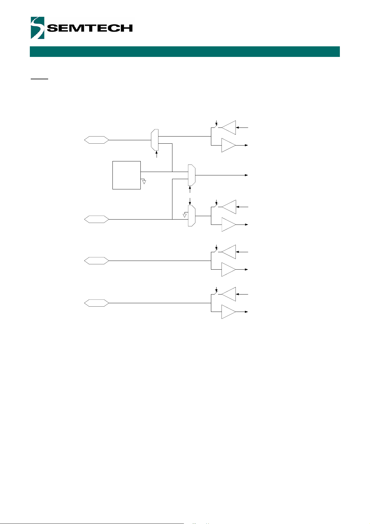
Block Diagram
AC2
AC3
AC4
AC5
AC6
AC7
D0/REF
D1/REF
D2
D3
SX8724
OUT
IN
V
BATT
2-WIRE
TM
READY
SCL
SDA
V
PUMP
VSS
+
-
+
V
REF
-
+
-
AC0
AC1
REF MUX
SIGNAL MUX
GPIO
PGA ADC
CONTROL LOGIC
CHARGE
PUMP
ZoomingADC
4MHz
OSC
Figure 3 - SX8724 Block Diagram
VREF
The internally generated V
stable voltage reference for the ZoomingADC.
This reference voltage is directly connected to one of the ZoomingADC reference multiplexer inputs.
The bandgap voltage stability is only guaranteed for V
2.4V, the bandgap voltage could reduce by up to 50mV.
The bandgap has relatively weak output drive so it is recommended that if the bandgap is required as a signal
input then PGA1 must be enabled with Gain = 1.
V1.23 © 2009 Semtech Corp. www.semtech.com
10
is a trimmed bandgap reference with a nominal value of 1.22V that provides a
REF
voltages of 3V and above. As V
BATT
drops down to
BATT
SX8724
ZoomingADC™ for Pressure and Temperature Sensing
ADVANCED COMMUNICATIONS & SENSING
GPIO
The GPIO block is a multipurpose 4 bit input/output port. In addition to digital behavior, D0 and D1 pins can be
programmed as analog pins in order to be used as output (reference voltage monitoring) and input for an
external reference voltage (For further details see Figure 14, Figure 15, Figure 16 and Figure 17). Each port
terminal can be individually selected as digital input or output.
D0/REF
OUT
0
1
RegMode[1]
RegOut[4]
RegOut[0]
RegIn[0]
D1/REF
D2
D3
+
V
REF
-
IN
0
1
RegMode[0]
1
0
ZoomingADC
RegOut[5]
RegOut[1]
RegIn[1]
RegOut[6]
RegOut[2]
RegIn[2]
RegOut[7]
RegOut[3]
RegIn[3]
Figure 4 - GPIO Block Diagram
The direction of each bit within the GPIO block (input only or input/output) can be individually set using the 4
MSB bits of the RegOut register. If D[x]_DIR = 1, both the input and output buffer are active on the
corresponding GPIO block pin. If D[x]_DIR = 0, the corresponding GPIO block pin is an input only and the
output buffer is in high impedance. After power on reset the GPIO block pins are in input/output mode
(D[x]_DIR are reset to 1)
The input values of GPIO block are available in RegIn register (read only). Reading is always direct – there is
no debounce function in the GPIO block. In case of possible noise on input signals, an external hardware filter
has to be realized. The input buffer is also active when the GPIO block is defined as output and the effective
value on the pin can be read back.
Data stored in the 4 LSB bits of RegOut register are outputted at GPIO block if D[x]_DIR = 1. The default values
after power on reset is low (0).
The digital pins are able to deliver a driving current up to 8 mA.
When the bits VREF_D0_OUT and VREF_D1_IN in the RegMode register are set to 1 the D0 and D1 pins
digital behavior are automatically bypassed in order to either input or output the voltage reference signals.
V1.23 © 2009 Semtech Corp. www.semtech.com
11

SX8724
ZoomingADC™ for Pressure and Temperature Sensing
ADVANCED COMMUNICATIONS & SENSING
Charge Pump
This block generates a supply voltage able to power the analog switch drive levels on the chip.
The minimum acceptable switch supply is 3V which means that if V
be activated to generate a voltage of 3V or above. If V
straight through to the V
If control input bit MULT_FORCE_OFF = 1 in RegMode register then the charge pump is disabled and V
permanently connected to V
If control input bit MULT_FORCE_ON = 1 in RegMode register then the charge pump is permanently enabled.
This overrides MULT_FORCE_OFF bit in RegMode register.
If MULT_FORCE_ON = 0 and MULT_FORCE_OFF = 0 bits in RegMode register then the charge pump will
start if V
drops below 3V, otherwise V
BATT
These controls are supplied to give the user the option of fixing the charge pump state to avoid it turning off and
on when V
is close to 3V.
BATT
The cell will use the on-chip bandgap reference and comparator to detect when V
activated, the block will use the charge pump to boost the V
ensure that the generated voltage never exceeds 0.7V above V
An external capacitor is required on V
This capacitor should be large enough to ensure that generated voltage is smooth enough to avoid affecting
conversion accuracy but not so large that it gives an unacceptable settling time. A recommended value is
around 2.2nF.
The block will also indicate when the pumped output voltage is sufficiently high to allow ADC conversions to be
started. This will be a simple comparison which will give a ready signal when the V
PUMP
output.
PUMP
drops below 3V then the block should
is greater than 3V then V
BATT
BATT
may be switched
BATT
BATT
is
.
will be switched directly through to V
BATT
voltage to above 3V but with diode limiting to
BATT
.
BATT
whenever the power supply is supposed to be less or drop below 3V.
PUMP
.
PUMP
is too low. When
BATT
output is 3V or above.
PUMP
V1.23 © 2009 Semtech Corp. www.semtech.com
12

SX8724
ZoomingADC™ for Pressure and Temperature Sensing
ADVANCED COMMUNICATIONS & SENSING
RC Oscillator
This block provides the master clock reference for the chip. It produces a clock at 4 MHz which is divided
internally in order to generate the clock sources needed by the other blocks.
The oscillator technique is a low power relaxation design and it is designed to vary as little as possible over
temperature and supply voltage.
This oscillator is trimmed at manufacture chip test.
The RC oscillator will start up after a chip reset to allow the trimming values to be read and calibration registers
and 2-WIRE address set to their programmed values. Once this has been done, the oscillator will be shut down
and the chip will enter a sleep state while waiting for a 2-WIRE communication.
V1.23 © 2009 Semtech Corp. www.semtech.com
13

SX8724
ZoomingADC™ for Pressure and Temperature Sensing
ADVANCED COMMUNICATIONS & SENSING
2-WIRE
The 2-WIRE interface gives access to the chip registers. It complies with the 2-WIRE protocol specifications,
restricted to the slave side of the communication.
General features:
• Slave only operation
• Fast mode operation (up to 400 kHz)
• Combined read and write mode support
• General call reset support
• 7-bit device address customization
• Stretch 2-WIRE clock SCL only before sending ACK/NACK
The interface handles 2-WIRE communication at the transaction level: the processor is only aware of read and
writes transactions. A read transaction is an external request to get the content of system memory location and
a write transaction is an external request to write the content of a system memory location.
2-WIRE Communication Format
SDA
SCL
SDA
SCL
SDA
Ready
SDA
Ready
Start Slave Address ACK
1 0 0 1 0 0 0 0 0
1 9 1 9 1 9 1 9
Master Master Master MasterSX8724 SX8724SX8724
Start Slave Address ACK
1 0 0 1 0 0 0 0 0
1 9 1 9 1 9 1 9
Master SX8724 Master Master MasterSX8724 SX8724
Start Slave Address ACK
SCL
...
...
SCL
1 0 0 1 0 0 0 0 0
1 9 1 9 1 9 1 9
Master Master Master MasterSX8724 SX8724SX8724
Start Slave Address ACK
1 0 0 1 0 0 0 0 0
1 9 1 9 1 9 1 9
Master Master Master MasterSX8724 SX8724SX8724
Figure 7 - Timing Diagram for Reading an ADC Sample from SX8724
W
Figure 5 - Timing Diagram for Reading from SX8724
W
Figure 6 - Timing Diagram for Writing to the SX8724
W
W
Memory Address ACK Start Slave Address ACK
A7 A6 A5 A4 A3 A2 A1 A0 D7 D6 D5 D4 D3 D2 D1 D01 0 0 1 0 0 0 1
Memory Address ACK Start Slave Address ACK
A7 A6 A5 A4 A3 A2 A1 A0 D7 D6 D5 D4 D3 D2 D1 D01 0 0 1 0 0 0 0
RegACOutMsb ACK Start Slave Address ACK
0 D7 D6 D5 D4 D3 D2 D1 D01 0 0 1 0 0 0 1
0 0 0 0
1 1
RegACOutLsb ACK Start Slave Address ACK
0 D7 D6 D5 D4 D3 D2 D1 D01 0 0 1 0 0 0 1
0 0 0 0 0
1 1
1
R
W
R
R
SX8724
Data NACK Stop
Data ACK Stop
Master
Data NACK Stop
...
...
Data NACK Stop
2-WIRE Address
The default 2-WIRE slave address is 1001000 in binary.
This is the standard part 2-WIRE slave address. Other addresses between 1001001 and 1001111 are available
by special request.
V1.23 © 2009 Semtech Corp. www.semtech.com
14
SX8724
ZoomingADC™ for Pressure and Temperature Sensing
ADVANCED COMMUNICATIONS & SENSING
ZoomingADC
Features
The ZoomingADC is a complete and versatile low-power analog front-end interface typically intended for sensing
applications.
In the following text the ZoomingADC will be referred as ZADC.
The key features of the ZADC are:
• Programmable 6 to 16-bit dynamic range over-sampled ADC
• Flexible gain programming between 0.5 and 1000
• Flexible and large range offset compensation
• 4-channel differential or 7-channel single-ended input
• 2-channel differential reference inputs
• Power saving modes
Overview
Analog
Inputs
V
V
AC
AC
AC
AC
AC
AC
SS
REF
AC
AC
2
3
4
5
6
7
f
s
0
1
V
IN
PGA1 PGA2 PGA3
GD1
V
D1
GD2
V
D2
+
GD3
-
OFF2
OFF3
V
IN,ADC
+
-
f
ADC
s
16
Input
Selection
BATT
SS
REF
SS
+
V
+
-
REF,ADC
Gain 1 Gain 2 Offset 2 Gain 3 Offset 3
Reference
Inputs
V
V
V
V
Reference
Selection
ZOOM
Figure 8 - ZADC General Functional Block Diagram
The total acquisition chain consists of an input multiplexer, 3 programmable gain amplifier stages and an over
sampled A/D converter. The reference voltage can be selected on two different channels. Two offset compensation
amplifiers allow for a wide offset compensation range. The programmable gain and offset allow the application to
zoom in on a small portion of the reference voltage defined input range.
ZADC Description
Acquisition Chain
Figure 8
manages all communications with the 2-WIRE peripheral.
shows the general block diagram of the acquisition chain (AC).
The clocking is derived from the internal 4 MHz
A control block (not shown in Figure 8)
Oscillator.
Analog inputs can be selected through an 8 input multiplexer, while reference input is selected between two
differential channels. It should however be noted that only 7 acquisition channels (including the V
) are available
REF
when configured as single ended since the input amplifier is always operating in differential mode with both positive
and negative input selected through the multiplexer.
The core of the zooming section is made of three differential programmable amplifiers (PGA). After selection of an
input and reference signals
VIN and V
combination, the input voltage is modulated and amplified through
REF,ADC
V1.23 © 2009 Semtech Corp. www.semtech.com
15

SX8724
ZoomingADC™ for Pressure and Temperature Sensing
ADVANCED COMMUNICATIONS & SENSING
stages 1 to 3. Fine gain programming up to 1'000 V/V is possible. In addition, the last two stages provide
programmable offset. Each amplifier can be bypassed if needed.
The output of the PGA stages is directly fed to the analog-to-digital converter (ADC), which converts the signal
V
into digital.
IN,ADC
Like most ADCs intended for instrumentation or sensing applications, the ZoomingADC is an over-sampled
converter (See Note1). The ADC is a so-called incremental converter; with bipolar operation (the ADC accepts
both positive and negative differential input voltages). In first approximation, the ADC output result relative to
full-scale (FS) delivers the quantity:
OUT
F
S
ADC
V
≅
ADCIN
V
2/2/
,,ADCREF
Equation 1
in two's complement (see Equation 4 and Equation 5 for details). The output code OUT
V
IN,ADC
≅ -V
REF,ADC
/2 to +V
/2 respectively. As will be shown, V
REF,ADC
is related to input voltage VIN by the
IN,ADC
relationship:
VGDoffVGDV
⋅−⋅=
ADCREFTOTINTOTADCIN
,,
(V)
Equation 2
where GD
is the total PGA gain, and GDoff
TOT
is the total PGA offset.
TOT
is -FS/2 to +FS/2 for
ADC
1
Note: Over-sampled converters are operated with a sampling frequency fS much higher than the input signal's Nyquist rate (typically fS is
20-1'000 times the input signal bandwidth). The sampling frequency to throughput ratio is large (typically 10-500). These converters include
digital decimation filtering. They are mainly used for high resolution, and/or low-to-medium speed applications.
V1.23 © 2009 Semtech Corp. www.semtech.com
16

SX8724
ZoomingADC™ for Pressure and Temperature Sensing
ADVANCED COMMUNICATIONS & SENSING
Registers
The system has a bank of eight 8-bit registers: six registers are used to configure the acquisition chain
(RegAcCfg0 to 5), and two registers are used to store the output code of the analog-to-digital conversion
(RegAcOutMsb & Lsb).
Register Name
7 6 5 4 3 2 1 0
RegACOutLsb OUT[7:0]
RegACOutMsb OUT[15:8]
RegACCfg0
Default values:
RegACCfg1
Default values:
RegACCfg2
Default values:
RegACCfg3
Default values:
RegACCfg4
Default values:
RegACCfg5
Default values:
START
0
IB_AMP_ADC[1:0]
FIN[1:0]
PGA1_G
0
-
0
BUSY
0
SET_NELC[1:0]
11
00
DEF
0
01
IB_AMP_PGA[1:0]
11
PGA2_GAIN[1:0]
00
Bit Position
SET_OSR[2:0]
010
PGA3_GAIN[6:0]
0001100
PGA3_OFFSET[6:0]
0000000
AMUX[4:0]
00000
CONT
0
ENABLE[3:0]
0000
PGA2_OFFSET[3:0]
0000
-
0
VMUX
0
Table 1 - Peripheral Registers to Configure the Acquisition Chain (AC)
and to Store the Analog-to-Digital Conversion (ADC) Result
With:
• OUT: (r) digital output code of the analog-to-digital converter. (MSB = OUT[15])
• START: (w) setting this bit triggers a single conversion (after the current one is finished). This bit always reads back 0.
• SET_NELC: (rw) sets the number of elementary conversions to 2 SET_NELC[1:0]. To compensate for offsets, the input signal is
chopped between elementary conversions (1,2,4,8).
• SET_OSR: (rw) sets the over-sampling rate (OSR) of an elementary conversion to 2(3+SET_OSR[2:0]). OSR = 8, 16, 32, ..., 512,
1024.
• CONT: (rw) setting this bit starts a conversion. A new conversion will automatically begin as long as the bit remains at 1.
• TEST: bit only used for test purposes. In normal mode, this bit is forced to 0 and cannot be overwritten.
• IB_AMP_ADC: (rw) sets the bias current in the ADC to 0.25*(1+ IB_AMP_ADC[1:0]) of the normal operation current (25, 50, 75 or
100% of nominal current). To be used for low-power, low-speed operation.
• IB_AMP_PGA: (rw) sets the bias current in the PGAs to 0.25*(1+IB_AMP_PGA[1:0]) of the normal operation current (25, 50, 75 or
100% of nominal current). To be used for low-power, low-speed operation.
• ENABLE: (rw) enables the ADC modulator (bit 0) and the different stages of the PGAs (PGAi by bit i=1,2,3). PGA stages that are
disabled are bypassed.
• FIN: (rw) These bits set the over sampling frequency of the acquisition chain. Expressed as a fraction of the oscillator frequency,
the sampling frequency is given as: 11 500 kHz, 10 250 kHz, 01 125 kHz, 00 62.5 kHz.
• PGA1_GAIN: (rw) sets the gain of the first stage: 0 1, 1 10.
• PGA2_GAIN: (rw) sets the gain of the second stage: 00 1, 01 2, 10 5, 11 10.
• PGA3_GAIN: (rw) sets the gain of the third stage to PGA3_GAIN[6:0]⋅1/12.
• PGA2_OFFSET: (rw) sets the offset of the second stage between –1 and +1, with increments of 0.2. The MSB gives the sign
(0 → positive, 1 → negative); amplitude is coded with the bits PGA2_OFFSET[5:0].
• PGA3_OFFSET: (rw) sets the offset of the third stage between –5.25 and +5.25, with increments of 1/12. The MSB gives the sign
(0 → positive, 1 → negative); amplitude is coded with the bits PGA3_OFFSET[5:0].
• BUSY: (r) set to 1 if a conversion is running.
• DEF: (w) sets all values to their defaults (PGA disabled, max speed, nominal modulator bias current, 2 elementary conversions,
over-sampling rate of 32) and starts a new conversion without waiting the end of the preceding one.
• AMUX(4:0): (rw) AMUX(4) sets the mode (0 differential inputs, 1 single ended inputs with A0 = common reference) AMUX(3)
sets the sign (0 straight, 1 cross) AMUX(2:0) sets the channel.
• VMUX: (rw) sets the differential reference channel (0 V
(r = read; w = write; rw = read & write)
BATT
, 1 V
REF
).
V1.23 © 2009 Semtech Corp. www.semtech.com
17

SX8724
T
ZoomingADC™ for Pressure and Temperature Sensing
ADVANCED COMMUNICATIONS & SENSING
ZADC Detailed Functionality Description
Continuous-Time vs. On-Request
The ADC can be operated in two distinct modes: "continuous-time" and "on-request" modes (selected using the
bit CONT).
In "continuous-time" mode, the input signal is repeatedly converted into digital. After a conversion is finished, a
new one is automatically initiated. The new value is then written in the result register, and the corresponding
internal trigger pulse is generated. This operation is sketched in Figure 9. The conversion time in this case is
defined as T
CONV
.
Output Code
RegACOut[15:0]
CONV
Internal Trig
BUSY
IRQ/READY
Figure 9 - ADC "Continuous-Time" Operation
In the "on-request" mode, the internal behavior of the converter is the same as in the "continuous-time" mode,
but the conversion is initiated on user request (with the START bit). As shown in Figure 10, the conversion time
is also T
CONV
.
Figure 10 - ADC "On-Request" Operation
V1.23 © 2009 Semtech Corp. www.semtech.com
18

SX8724
ZoomingADC™ for Pressure and Temperature Sensing
ADVANCED COMMUNICATIONS & SENSING
Input Multiplexers
The ZoomingADC has eight analog inputs AC0 to AC7 and four reference inputs AC_R0 to AC_R3. Let us first
define the differential input voltage VIN and reference voltage V
and:
respectively as:
REF,ADC
VVV −=
(V)
INNINPIN
Equation 3
VVV −=
(V)
,
REFNREFPADCREF
Equation 4
As shown in Table 2, the inputs can be configured in two ways: either as 4 differential channels (V
AC0,..., V
= AC7 - AC6), or AC0 can be used as a common reference, providing 7 signal paths all referred to
IN4
= AC1 -
IN1
AC0. The control word for the analog input selection is AMUX[4:0]. Notice that the bit AMUX[3] controls the sign
of the input voltage.
AMUX[4:0]
(RegACCfg5[5:1])
00x00 AC1 (V
00x01 AC3 AC2
00x10 AC5 AC4
00x11 AC7 AC6
10000 AC0 (VSS)
10001 AC1 (V
10010 AC2
10011 AC3
10100 AC4
10101 AC5
10110 AC6
10111 AC7
V
V
INP
) AC0 (VSS)
REF
)
REF
INN
AC0 (VSS)
AMUX[4:0]
(RegACCfg5[5:1])
01x00 AC0 (VSS) AC1 (V
01x01 AC2 AC3
01x10 AC4 AC5
01x11 AC6 AC7
11000 AC0 (VSS)
11001 AC1 (V
11010 AC2
11011 AC3
11100 AC4
11101 AC5
11110 AC6
11111
V
V
INP
AC0 (VSS)
INN
AC7
REF
REF
)
)
Table 2 - Analog Input Selection
Similarly, the reference voltage is chosen among two differential channels (V
V
V
= AC_R3 - AC_R2) as shown in Table 3. The selection bit is VMUX. The reference inputs V
REF,ADC
(common-mode) can be up to the power supply range.
REFN
= AC_R1 - AC_R0 or
REF,ADC
REFP
and
VMUX
(RegACCfg5[0])
0
1
V
REFP
AC_R1 (V
AC_R3 (V
V
BATT
REF
)
)
AC_R0 (VSS)
AC_R2 (VSS)
REFN
Table 3 - Analog Reference Input Selection
V1.23 © 2009 Semtech Corp. www.semtech.com
19

SX8724
ZoomingADC™ for Pressure and Temperature Sensing
ADVANCED COMMUNICATIONS & SENSING
Programmable Gain Amplifiers
As seen in Figure 8, the zooming function is implemented with three programmable gain amplifiers (PGA).
These are:
• PGA1: coarse gain tuning
• PGA2: medium gain and offset tuning
• PGA3: fine gain and offset tuning. Should be set ON for high linearity data acquisition
All gain and offset settings are realized with ratios of capacitors. The user has control over each PGA activation
and gain, as well as the offset of stages 2 and 3. These functions are examined hereafter.
ENABLE[3:0]
(RegACCfg1[3:0])
xxx0 ADC disabled
xxx1 ADC enabled
xx0x PGA1 disabled
xx1x PGA1 enabled
x0xx PGA2 disabled
x1xx PGA2 enabled
0xxx PGA3 disabled
1xxx PGA3 enabled
Table 4 - ADC & PGA Enabling
PGA1_GAIN
(RegACCfg3[7])
0 1
1 10
Table 5 - PGA1 Gain Settings
PGA2_GAIN[1:0]
(RegACCfg2[5:4])
00 1
01 2
10 5
11 10
Table 6 - PGA2 Gain Settings
PGA2_OFFSET[3:0]
(RegACCfg2[3:0])
0000 0
0001 +0.2
0010 +0.4
0011 +0.6
0100 +0.8
0101 +1
1001 -0.2
1010 -0.4
1011 -0.6
1100 -0.8
1101 -1
Block
PGA1 Gain
GD1 (V/V)
PGA2 Gain
GD2 (V/V)
PGA2 Offset
GDoff2 (V/V)
PGA3_GAIN[6:0]
(RegACCfg3[6:0])
0000000 0
0000001 1/12(=0.083)
... ...
0000110 6/12
... ...
0001100 12/12
0010000 16/12
...
0100000 32/12
...
1000000 64/12
...
1111111 127/12(=10.58)
PGA3 Gain
GD3 (V/V)
Table 8 - PGA3 Gain Settings
PGA3_OFFSET[6:0]
(RegACCfg4[6:0])
0000000 0
0000001 +1/12(=+0.083)
0000010 +2/12
... ...
0010000 +16/12
... ...
0100000 +32/12
... ...
0111111 +63/12(=+5.25)
1000000 0
1000001 -1/12(=-0.083)
1000010 -2/12
... ...
1010000 -16/12
... ...
1100000 -32/12
... ...
1111111 -63/12(=-5.25)
Table 9 - PGA3 Offset Settings
PGA3 Offset
GDoff3 (V/V)
Table 7 - PGA2 Offset Settings
V1.23 © 2009 Semtech Corp. www.semtech.com
20

SX8724
ZoomingADC™ for Pressure and Temperature Sensing
ADVANCED COMMUNICATIONS & SENSING
PGA & ADC Enabling
Depending on the application objectives, the user may enable or bypass each PGA stage. This is done
according to the word ENABLE and the coding given in Table 4. To reduce power dissipation, the ADC can also
be inactivated while idle.
PGA1
The first stage can have a buffer function (unity gain) or provide a gain of 10 (see Table 5). The voltage VD1 at
the output of PGA1 is:
where GD1 is the gain of PGA1 (in V/V) controlled with the bit PGA1_GAIN.
PGA2
The second PGA has a finer gain and offset tuning capability, as shown in Table 6 and Table 7. The voltage VD2
at the output of PGA2 is given by:
VGDV ⋅=
(V)
IND
11
Equation 5
VGDoffVGDV
⋅−⋅=
,2122
ADCREFDD
(V)
Equation 6
where GD2 and GDoff2 are respectively the gain and offset of PGA2 (in V/V). These are controlled with the
words PGA2_GAIN[1:0] and PGA2_OFFSET[3:0].
PGA3
The finest gain and offset tuning is performed with the third and last PGA stage, according to the coding of
Table 8 and Table 9. The output of PGA3 is also the input of the ADC. Thus, similarly to PGA2, we find that the
voltage entering the ADC is given by:
VGDoffVGDV
⋅−⋅=
(V)
ADCREFDADCIN
,323,
Equation 7
where GD3 and GDoff3 are respectively the gain and offset of PGA3 (in V/V). The control words are
PGA3_GAIN[6:0] and PGA3_OFFSET[6:0]. To remain within the signal compliance of the PGA stages, the
condition:
,
VVV <
(V)
DDDD
21
Equation 8
must be verified.
Finally, combining equations 5 to 7 for the three PGA stages, the input voltage V
of the ADC is related to
IN,ADC
VIN by:
VGDoffVGDV
⋅−⋅=
ADCREFTOTINTOTADCIN
,,
(V)
Equation 9
where the total PGA gain is defined as:
GDGDGDGD
⋅⋅=
(V/V)
TOT
123
Equation 10
and the total PGA offset is:
TOT
⋅+=
(V/V)
233
GDoffGDGDoffGDoff
Equation 11
V1.23 © 2009 Semtech Corp. www.semtech.com
21

SX8724
(
)
+
ZoomingADC™ for Pressure and Temperature Sensing
ADVANCED COMMUNICATIONS & SENSING
ADC Characteristics
The main performance characteristics of the ADC (resolution, conversion time, etc.) are determined by three
programmable parameters. The setting of these parameters and the resulting performances are described later.
• Over-sampling frequency fs
• Over-Sampling Ratio OSR
• Number of Elementary Conversions NELCONV
Conversion Sequence
A conversion is started each time the bit START or the bit DEF is set. As depicted in Figure 11, a complete
analog-to-digital conversion sequence is made of a set of N
final quantization step. Each elementary conversion is made of (OSR+1) over-sampling periods Ts=1/fs, i.e.:
The result is the mean of the elementary conversion results. An important feature is that the elementary
conversions are alternatively performed with the offset of the internal amplifiers contributing in one direction and
the other to the output code. Thus, converter internal offset is eliminated if at least two elementary sequences
are performed (i.e. if N
≥ 2). A few additional clock cycles are also required to initiate and end the
ELCONV
conversion properly.
elementary incremental conversions and a
ELCONV
T
ELCONV
=
OSR
fs
1
(s)
Equation 12
Init
Conversion index
Offset
Elementary
Conversion
1 2 N
+ - + -
Elementary
Conversion
T
CONV
Elementary
Conversion
-1 N
ELCONV
Elementary
Conversion
ELCONV
End
Conversion
Result
Figure 11 - Analog-to-Digital Conversion Sequence
Note:
The internal bandgap reference state may be forced High or Low, or may be set to toggle during conversion at either the same rate or half
the rate of the Elementary Conversion. This may be useful to help eliminate bandgap related internal offset voltage and 1/fs noise.
Over-Sampling Frequency
The word FIN[1:0] (see Table 10) is used to select the over-sampling frequency fs. The over-sampling frequency
is derived from the 4MHz oscillator clock.
FIN[1:0]
(RegACCfg2[7:6])
00 62.5 kHz
01 125 kHz
10 250 kHz
11 500 kHz
Over-Sampling Frequency fs (Hz)
Table 10 - Over-Sampling Frequency Settings
V1.23 © 2009 Semtech Corp. www.semtech.com
22

SX8724
[
]
[
]
ZoomingADC™ for Pressure and Temperature Sensing
ADVANCED COMMUNICATIONS & SENSING
Over-Sampling Ratio
The over-sampling ratio (OSR) defines the number of integration cycles per elementary conversion. Its value is
set with the word SET_OSR[2:0] in power of 2 steps (see Table 11) given by:
0:2_3
OSR+=
2
OSRSET
Equation 13
SET_OSR[2:0]
(RegACCfg0[4:2])
000 8
001 16
010 32
011 64
100 128
101 256
110 512
111 1024
Over-Sampling Ratio
OSR (-)
Table 11 - Over-Sampling Ratio Settings
Elementary Conversions
As mentioned previously, the whole conversion sequence is made of a set of N
elementary incremental
ELCONV
conversions. This number is set with the word SET_NELC[1:0] in power of 2 steps (see Table 12) given by:
N =
ELCONV
0:1_2NELCSET
Equation 14
SET_NELC[1:0]
(RegACCfg0[6:5])
00 1
01 2
10 4
11 8
# of Elementary
Conversions
N
ELCONV
(-)
Table 12 - Number of Elementary Conversion Settings
As already mentioned, N
must be equal or greater than 2 to reduce internal amplifier offsets.
ELCONV
V1.23 © 2009 Semtech Corp. www.semtech.com
23

SX8724
()(
)
SET_OSR
SET_NELC=
ZoomingADC™ for Pressure and Temperature Sensing
ADVANCED COMMUNICATIONS & SENSING
Resolution
The theoretical resolution of the ADC, without considering thermal noise, is given by:
NOSRn
loglog2 +⋅=
22
ELCONV
Equation 15
17
15
13
11
9
7
5
000 001 010 011 100 101 110 111
11
10
01
00
(Bits)
Figure 12 - Resolution vs. SET_OSR[2:0] and SET_NELC[1:0]
Using look-up Table 13 or the graph plotted in Figure 12, resolution can be set between 6 and 16 bits. Notice
that, because of 16-bit register use for the ADC output, practically the resolution is limited to 16 bits,
i.e. n ≤ 16. Even though the resolution is truncated to 16 bit by the output register size, it may make sense to set
OSR and N
to higher values in order to reduce the influence of the thermal noise in the PGA and of
ELCONV
external noises (see section “PGA Gain & Offset, Linearity and Noise” in page 37).
SET_OSR
[2:0]
000 6 7 8 9
001 8 9 10 11
010 10 11 12 13
011 12 13 14 15
100 14 15 16 16
101 16 16 16 16
110 16 16 16 16
111 16 16 16 16
Note: shaded area: resolution truncated to 16 bits due to
output register size RegACOut[15:0]
00 01 10 11
SET_NELC[1:0]
Table 13 - Resolution vs. SET_OSR[2:0] and SET_NELC[1:0] Settings
V1.23 © 2009 Semtech Corp. www.semtech.com
24

SX8724
(
)
++⋅
01
ZoomingADC™ for Pressure and Temperature Sensing
T
CONV
ELCONV
=
OSRN
f
s
11
(s)
Equation 16
ADVANCED COMMUNICATIONS & SENSING
Conversion Time and Throughput
As explained in Figure 12, conversion time is given by:
and throughput is then simply 1/T
. For example, consider an over-sampling ratio of 256, 2 elementary
CONV
conversions, and a over-sampling frequency of 500kHz (SET_OSR = "101", SET_NELC = "01", FIN = "00"). In
this case, using Table 14, the conversion time is 515 over-sampling periods, or 1.03ms. This corresponds to a
throughput of 971Hz in continuous-time mode. The plot of Figure 7 illustrates the classic trade-off between
resolution and conversion time.
SET_NELC[1:0] SET_OSR
[2:0]
000 10 19 37 73
001 18 35 69 137
010 34 67 133 265
011 66 131 261 521
100 130 259 517 1033
101 258 515 1029 2057
110 514 1027 2053 4105
111 1026 2051 4101 8201
Table 14 - Normalized Conversion Time (T
00 01 10 11
) vs. SET_OSR[2:0] and SET_NELC[1:0]
CONV*fs
(Normalized to Over-Sampling Period 1/fs)
Note
Some high sample rate configurations can not be used due to 2-WIRE speed limitation.
16.0
14.0
12.0
10.0
8.0
Resolution - n [Bits]
6.0
4.0
10.0 100.0 1000.0 10000.0
10
00
Normalized Conversion Time - T
11
SET_NELC
CONV*fS
[-]
Figure 13 - Resolution vs. Normalized Conversion Time for Different SET_NELC[1:0]
V1.23 © 2009 Semtech Corp. www.semtech.com
25
SX8724
ZoomingADC™ for Pressure and Temperature Sensing
OUT
V
V
ADC
IN
ADCREF
,
TOT
+0.5⋅FS
-0.5⋅FS
TOT
16
2
V
V
OSR
ADCIN
,
⋅⋅=
ADCREF
,
Equation 17
GDoffGD
Equation 18
GDGDGDGD
⋅⋅=
1
+
(LSB)
OSR
V
⋅−⋅⋅=
TOTTOT
(V/V)
123
GDoffGDGDoffGDoff
⋅+=
+215-1=+32'767 7FFF
-215=-32'768 8000
ADCREF
,
V
IN
(V/V)
233
OSR
⋅
OSR
1
+
(LSB)
ADVANCED COMMUNICATIONS & SENSING
Output Code Format
The ADC output code is a 16-bit word in two's complement format (see Table 15). For input voltages outside the
range, the output code is saturated to the closest full-scale value (i.e. 0x7FFF or 0x8000). For resolutions
smaller than 16 bits, the non-significant bits are forced to the values shown in Table 16. The output code,
expressed in LSBs, corresponds to:
Recalling equation 9, this can be rewritten as:
OUT
ADC
16
2
where, from Equation 10and Equation 11, the total PGA gain and offset are respectively:
and:
ADC Input Voltage V
+2.46146V
+2.46138V ... +215-2=+32'766 7FFE
... ... ... ...
+75µV ... +1 0001
0V 0 0 0000
-75µV ... -1 8FFF
... ... ... ...
-2.46146V ... -215-1=-32'767 8001
-2.46154V
% of Full Scale (FS) Output in LSBs Output Code in Hex
IN,ADC
Table 15 - Basic ADC Relationships (example for: V
SET_OSR[2:0] SET_NELC = 00 SET_NELC = 01 SET_NELC = 10 SET_NELC = 11
000 1000000000 100000000 10000000 1000000
001 10000000 1000000 100000 10000
010 100000 10000 1000 100
011 1000 100 10 1
100 10 1 - 101 - - - 110 - - - 111 - - - -
= 5V, OSR = 64, n = 16 bits)
REF,ADC
Table 16 - Last Forced LSBs in Conversion Output Registers for Resolution Settings Smaller than 16
bits (n < 16) (RegACOutMsb[7:0] & RegACOutLsb[7:0])
V1.23 © 2009 Semtech Corp. www.semtech.com
26
SX8724
1
2
OSR
ZoomingADC™ for Pressure and Temperature Sensing
ADVANCED COMMUNICATIONS & SENSING
The equivalent LSB size at the input of the PGA chain is:
LSB
V
1
n
GD
,
TOT
Equation 19
⋅⋅=
OSR
OSR
(V)
12
+
ADCREF
Notice that the input voltage V
of the ADC must satisfy the condition:
IN,ADC
1
,
( )
VVV
REFNREFPADCIN
⋅−⋅≤
OSR
(V)
+
Equation 20
to remain within the ADC input range.
Power Saving Modes
During low-speed operation, the bias current in the PGAs and ADC can be programmed to save power using
the control words IB_AMP_PGA[1:0] and IB_AMP_ADC[1:0] (see Table 17). If the system is idle, the PGAs and
ADC can even be disabled, thus, reducing power consumption to its minimum. This can considerably improve
battery life.
IB_AMP_ADC[1:0]
(RegACCfg1[7:6])
00
01
11
x
IB_AMP_PGA[1:0]
(RegACCfg1[5:4])
x
00
01
11
ADC Bias Current PGA Bias Current Max. fs [kHz]
1/4⋅IADC
1/2⋅ IADC
IADC
x
x
1/4⋅IPGA
1/2⋅ IPGA
IPGA 500
125
250
500
125
250
Table 17 - ADC & PGA Power Saving Modes and Maximum Sampling Frequency
V1.23 © 2009 Semtech Corp. www.semtech.com
27

SX8724
ZoomingADC™ for Pressure and Temperature Sensing
ADVANCED COMMUNICATIONS & SENSING
Registers Map
Address Register Bits Description
RC Register
0x30 RegRCen 1 RC oscillator control
GPIO Registers
0x40 RegOut 8 D0 to D3 pads data output and direction control
0x41 RegIn 4 D0 to D3 pads input data
ADC Registers
0x50 RegACOutLsb 8 LSB of the ADC result
0x51 RegACOutMsb 8 MSB of the ADC result
0x52 RegACCfg0 7 ADC conversion control
0x53 RegACCfg1 8 ADC conversion control
0x54 RegACCfg2 8 ADC conversion control
0x55 RegACCfg3 8 ADC conversion control
0x56 RegACCfg4 7 ADC conversion control
0x57 RegACCfg5 8 ADC conversion control
Mode Register
0x70 RegMode 6 Chip operating mode register
Registers Descriptions
The register descriptions are presented here in ascending order of Register Address. Some registers carry
several individual data fields of various sizes; from single-bit values (e.g. flags), upwards. Some data fields are
spread across multiple registers. Unused bits are ‘don't care’ and writing either 0 or 1 will not affect any function
of the device. After power on reset the registers will have the values indicated in the tables “Reset” column.
RC Register
Bit Name Mode Reset Description
7:1 - r 000000 unused
0 RC_EN rw 1 Enables RC oscillator. Set 0 for low power mode.
Table 18 - RegRCen (0x30)
V1.23 © 2009 Semtech Corp. www.semtech.com
28

SX8724
ZoomingADC™ for Pressure and Temperature Sensing
ADVANCED COMMUNICATIONS & SENSING
GPIO Registers
Bit Name Mode Reset Description
7 D3_DIR rw 1 D3 pad direction: 1 = Output 0 = Input
6 D2_DIR rw 1 D2 pad direction: 1 = Output 0 = Input
5 D1_DIR rw 1 D1 pad direction: 1 = Output 0 = Input
4 D0_DIR rw 1 D0 pad direction: 1 = Output 0 = Input
3 D3_OUT rw 0 D3 pad output value. Only valid when D3_DIR = 1
2 D2_OUT rw 0 D2 pad output value. Only valid when D2_DIR = 1
1 D1_OUT rw 0 D1 pad output value. Only valid when D1_DIR = 1 and VREF_D1_IN = 0
0 D0_OUT rw 0
Bit Name Mode Reset Description
7:4 - r 0000 Unused
3 D3_IN r - D3 pad value
2 D2_IN r - D2 pad value
1 D1_IN r - D1 pad value
0 D0_IN r - D0 pad value
D0 pad output value. Only valid when D0_DIR = 1 and
VREF_D0_OUT = 0
Table - 19 RegOut (0x40)
Table - 20 RegIn (0x41)
V1.23 © 2009 Semtech Corp. www.semtech.com
29

SX8724
ZoomingADC™ for Pressure and Temperature Sensing
ADVANCED COMMUNICATIONS & SENSING
ZADC Registers
Bit Name Mode Reset Description
7:0 OUT[7:0] r 00000000 LSB of the ADC result
Bit Name Mode Reset Description
7:0 OUT[15:8] r 00000000 MSB of the ADC result
Bit Name Mode Reset Description
7 START rw 0 Starts an ADC conversion
6:5 SET_NELC[1:0] rw 01 Sets the number of elementary conversions
4:2 SET_OSR[2:0] rw 010 Sets the ADC over-sampling rate
1 CONT rw 0 Sets continuos ADC conversion mode
0 - r 0 unused
Table 21 - RegACOutLsb (0x50)
Table 22 - RegACOutMsb (0x51)
Table 23 - RegACCfg0 (0x52)
Bit Name Mode Reset Description
7:6 IB_AMP_ADC[1:0] rw 11 Bias current selection for the ADC
5:4 IB_AMP_PGA[1:0] rw 11 Bias current selection for the PGA
3:0 ENABLE[3:0] rw 0000 ADC and PGA stage enables
Table 24 - RegACCfg1 (0x53)
Bit Name Mode Reset Description
7:6 FIN[1:0] rw 00 ADC Sampling Frequency selection
5:4 PGA2_GAIN[1:0] rw 00 PGA2 gain selection
3:0 PGA2_OFFSET[3:0] rw 0000 PGA2 offset selection
Table 25 - RegACCfg2 (0x54)
Bit Name Mode Reset Description
7 PGA1_GAIN rw 0 PGA1 gain selection
6:0 PGA3_GAIN[6:0] rw 0001100 PGA3 gain selection
Table 26 - RegACCfg3 (0x55)
Bit Name Mode Reset Description
7 -
6:0 PGA3_OFFSET[6:0] rw 0000000 PGA3 offset selection
Table 27 - RegACCfg4 (0x56)
Bit Name Mode Reset Description
7 BUSY r 0 ADC activity flag
6 DEF rw 0 Selects ADC & PGA default configuration
5:1 AMUX[4:0] rw 00000 Input channel configuration selector
0 VMUX rw 0 Reference source selector (V
BATT
= 0 or V
REF
= 1)
Table 28 - RegACCfg5 (0x57)
V1.23 © 2009 Semtech Corp. www.semtech.com
30

SX8724
ZoomingADC™ for Pressure and Temperature Sensing
ADVANCED COMMUNICATIONS & SENSING
Mode Register
Bit Name Mode Reset Function
7 MULT_READY r 1
6 MULT_ACTIVE r 0
5:4 CHOP rw 00 VREF chopping control
3 MULT_FORCE_ON rw 0 Force charge pump On (takes priority) (Note 2)
2 MULT_FORCE_OFF rw 1 Force charge pump Off (Note 2)
1 VREF_D0_OUT rw 0 Enable VREF output on D0 pin
0 VREF_D1_IN rw 0 Enable VREF input on D1 pin
Note1: The chop control is to allow chopping of the internal bandgap reference. This may be useful to help eliminate bandgap
Note2: The internal charge pump may be forced On or Off to avoid conversion interruptions due to the pump switching off and on
related internal offset voltage and 1/f noise. The bandgap chop state may be forced High or Low, or may be set to toggle
during conversion at either the same rate or half the rate of the Elementary Conversion. (See Conversion Sequence in the
ZoomingADC description)
when the V
sufficient supply to the ADC. If the ADC is not being run at full rate or full accuracy then it may operate sufficiently well
when V
supply is near 3V. If the pump is on automatic, then it will activate when V
BATT
is less than 3V.
BATT
1: Indicates that the charge pump has settled and the output voltage is
sufficient for conversion
1: Indicates that the charge pump is running (either because VBATT<3V
or it has been forced on)
11: Chop at Nelconv/2 rate
10: Chop at Nelconv rate
01: Chop state = 1
00: Chop state = 0
(Note 1)
Table 29 - RegMode (0x70)
drops below 3V to ensure
BATT
V1.23 © 2009 Semtech Corp. www.semtech.com
31

SX8724
ZoomingADC™ for Pressure and Temperature Sensing
ADVANCED COMMUNICATIONS & SENSING
Optional Operating Modes: External Voltage Reference Option
D0 and D1 are multi-functional pins with the following functions in different operating modes (see RegMode
register for control settings):
RegMode[1] = 0
+
-
0
1
0
1
RegMode[0] = 0
1
0
D0/REF
D1/REF
OUT
V
REF
IN
Figure 14 - D0 and D1 are Digital Inputs /
Outputs
GPIO
ZoomingADC
GPIO
D0/REF
OUT
V
REF
D1/REF
IN
Figure 16 - D0 is Reference Voltage Output and
D1 is Digital Input / Output
RegMode[1] = 1
+
-
0
1
0
1
RegMode[0] = 0
1
0
GPIO
ZoomingADC
GPIO
D0/REF
D1/REF
RegMode[1] = 1
+
-
0
1
0
1
RegMode[0] = 1
1
0
D0/REF
D1/REF
OUT
V
REF
IN
RegMode[1] = 0
+
-
0
1
0
1
RegMode[0] = 1
1
0
OUT
V
REF
IN
GPIO
ZoomingADC
GPIO
GPIO
ZoomingADC
GPIO
Figure 17 - D0 is Reference Voltage Output and
Figure 15 - D0 is Digital Input / Output and D1
Reference Voltage Input
D1 is Reference Voltage Input
This allows external monitoring of the internal bandgap reference or the ability to use an external reference input
for the ADC, or the option to filter the internal V
output before feeding back as V
REF
REF,ADC
input.
The internally generated V
When using an external V
is a trimmed bandgap reference with a nominal value of 1.22V.
REF
input, it may have any value between 0V and V
REF,ADC
. Simply substitute
BATT
the external value for 1.22 V in the ADC conversion calculations.
V1.23 © 2009 Semtech Corp. www.semtech.com
32

SX8724
ZoomingADC™ for Pressure and Temperature Sensing
ADVANCED COMMUNICATIONS & SENSING
Application Hints
Recommended Operation Mode and Registers Settings
Operation Mode
Parameter Value Units
VMUX VBATT
AMUX VINP = AC3 & VINN = AC2
PGA1 Gain OFF V/V
PGA2 Gain OFF V/V
PGA3 Gain 1 V/V
Total Offset 0 V/V
PGA2 Offset OFF V/V
PGA3 Offset 0 V/V
ADC Bias 50 %
PGA Bias 50 %
fs 250 kHz
Resolution 16 Bits
OSR 512 OverSamples / ElementaryConversion
NELCONV 2 ElementaryConversion / Conversion
Continuous mode ON -
Analog multiplexers
PGA
ADC
Table 30 - Recommended Operation Mode Values
Registers Settings
Register Name
RegACOutLsb OUT[7:0] XXXXXXXX
RegACOutMsb OUT[15:8] XXXXXXXX
RegACCfg0
RegACCfg1
RegACCfg2
RegACCfg3
RegACCfg4
RegACCfg5
7 6 5 4 3 2 1 0
START
0
IB_AMP_ADC[1:0]
PGA1_G
0
-
0
BUSY
0
01
FIN[1:0]
10
SET_NELC[1:0]
01
IB_AMP_PGA[1:0]
PGA2_GAIN[1:0]
DEF
0
Bit Position
01
SET_OSR[2:0]
110
PGA2_OFFSET[3:0]
PGA3_GAIN[6:0]
0001100
PGA3_OFFSET[6:0]
0000000
AMUX[4:0]
00001
CONT
1
ENABLE[3:0]
1001
0000
-
0
VMUX
0
Hexadecimal
Value
0x3A
0x59
0x80
0x0C
0x00
0x02
Table 31 - Registers Settings
V1.23 © 2009 Semtech Corp. www.semtech.com
33

SX8724
ZoomingADC™ for Pressure and Temperature Sensing
ADVANCED COMMUNICATIONS & SENSING
Schematic
REF MUX
SIGNAL MUX
Figure 18 - Recommended Operation Mode Schematic
V1.23 © 2009 Semtech Corp. www.semtech.com
34

SX8724
ZoomingADC™ for Pressure and Temperature Sensing
ADVANCED COMMUNICATIONS & SENSING
Input Impedance
The PGAs of the ZoomingADC are a switched capacitor based blocks (see Switched Capacitor Principle
chapter). This means that it does not use resistors to fix gains, but capacitors and switches. This has important
implications on the nature of the input impedance of the block.
Using switched capacitors is the reason why, while a conversion is done, the input impedance on the selected
channel of the PGAs is inversely proportional to the sampling frequency fs and to stage gain as given in
Equation 21.
The input impedance observed is the input impedance of the first PGA stage that is enabled or the input
impedance of the ADC if all three stages are disabled.
PGA1 (with a gain of 10), PGA2 (with a gain of 10) and PGA3 (with a gain of 10) each have a minimum input
impedance of 150 kΩ at fs = 500 kHz (see ZoomingADC Specifications). Larger input impedance can be
obtained by reducing the gain and/or by reducing the sampling frequency. Therefore, with a gain of 1 and a
sampling frequency of 125 kHz, Zin > 6.1MΩ.
The input impedance on channels that are not selected is very high (>100MΩ).
9
Hz
Ω⋅
Z
≥
in
10768
gainf
⋅
s
Equation 21
(Ω)
V1.23 © 2009 Semtech Corp. www.semtech.com
35

SX8724
R
−
(
)
ZoomingADC™ for Pressure and Temperature Sensing
ADVANCED COMMUNICATIONS & SENSING
Switched Capacitor Principle
Basically, a switched capacitor is a way to emulate a resistor by using a capacitor. The capacitors are much
easier to realize on CMOS technologies and they show a very good matching precision.
V
V
1
V
2
R
1
ff V
2
Figure 19 - The Switched Capacitor Principle
A resistor is characterized by the current that flows through it (positive current leaves node V1):
VV
I
=
21
(A)
Equation 22
One can verify that the mean current leaving node V1 with a capacitor switched at frequency f is:
CfVVI ⋅⋅−= 21
(A)
Equation 23
Therefore as a mean value, the switched capacitor
1
is equivalent to a resistor.
Cf ⋅
It is important to consider that this is only a mean value. If the current is not integrated (low impedance source),
the impedance is infinite during the whole time but the transition.
What does it mean for the ZoomingADC?
If the fs clock is reduced, the mean impedance is increased. By dividing the fs clock by a factor 10, the
impedance is increased by a factor 10.
One can reduce the capacitor that is switched by using an amplifier set to its minimal gain. In particular if PGA1
is used with gain 1, its mean impedance is 10x bigger than when it is used with gain 10.
Current
integration
Sensor
impedence
ZoomingADC (model)
V
1
ff V
2
Sensor
Node
Capacitance
C
Figure 20 - The Switched Capacitor Principle
One can increase the effective impedance by increasing the electrical bandwidth of the sensor node so that the
switching current is absorbed through the sensor before the switching period is over. Measuring the sensor
node will show short voltage spikes at the frequency fs, but these will not influence the measurement. Whereas
if the bandwidth of the node is lower, no spikes will arise, but a small offset can be generated by the integration
of the charges generated by the switched capacitors, this corresponds to the mean impedance effect.
Note:
One can increase the mean input impedance of the ZoomingADC by lowering the acquisition clock fs.
One can increase the mean input impedance of the ZoomingADC by decreasing the gain of the first enabled amplifier.
One can increase the effective input impedance of the ZoomingADC by having a source with a high electrical bandwidth (sensor electrical
bandwidth much higher than fs).
V1.23 © 2009 Semtech Corp. www.semtech.com
36

SX8724
ZoomingADC™ for Pressure and Temperature Sensing
ADVANCED COMMUNICATIONS & SENSING
PGA Settling or Input Channel Modifications
PGAs are reset after each writing operation to registers RegAcCfg1-5. Similarly, input channels are switched
after modifications of AMUX[4:0] or VMUX. To ensure precise conversion, the ADC must be started after a PGA
or inputs common-mode stabilization delay. This is done by writing bit START several cycles after PGA settings
modification or channel switching. Delay between PGA start or input channel switching and ADC start should be
equivalent to OSR (between 8 and 1024) number of cycles. This delay does not apply to conversions made
without the PGAs.
If the ADC is not settled within the specified period, there is most probably an input impedance problem (see
previous section).
PGA Gain & Offset, Linearity and Noise
Hereafter are a few design guidelines that should be taken into account when using the ZoomingADC:
1. Keep in mind that increasing the overall PGA gain, or "zooming" coefficient, improves linearity but
degrades noise performance.
2. Use the minimum number of PGA stages necessary to produce the desired gain ("zooming") and offset.
Bypass unnecessary PGAs.
3. Put most gain on PGA3 and use PGA2 and PGA1 only if necessary.
4. PGA3 should be always ON for best linearity.
5. For low-noise applications where power consumption is not a primary concern, maintain the largest bias
currents in the PGAs and in the ADC; i.e. set IB_AMP_PGA[1:0] = IB_AMP_ADC[1:0] = '11'.
6. For lowest output offset error at the output of the ADC, bypass PGA2 and PGA3. Indeed, PGA2 and
PGA3 typically introduce an offset of about 5 to 10 LSB (16 bit) at their output. Note, however, that the
ADC output offset is easily calibrated out by software.
V1.23 © 2009 Semtech Corp. www.semtech.com
37

SX8724
⋅
Normalized Magnitude [-]
Normalized Magnitude [-]
Normalized Magnitude [-]
Normalized Magnitude [-]
ZoomingADC™ for Pressure and Temperature Sensing
ADVANCED COMMUNICATIONS & SENSING
Frequency Response
The incremental ADC is an over-sampled converter with two main blocks: an analog modulator and a low-pass
digital filter. The main function of the digital filter is to remove the quantization noise introduced by the
modulator. This filter determines the frequency response of the transfer function between the output of the ADC
and the analog input VIN. Notice that the frequency axes are normalized to one elementary conversion period
OSR / fs. The plots of Figure 21 also show that the frequency response changes with the number of elementary
conversions N
and are repeated every fs / OSR.
Information on the location of these notches is particularly useful when specific frequencies must be filtered out
by the acquisition system. This chip has no dedicated 50/60 Hz rejection filtering but some rejection can be
achieved by using Equation 24 and setting the appropriate values of OSR, fs and
Examples:
Rejection [Hz] f
60
50
performed. In particular, notches appear for N
ELCONV
NOTCH
NOTCH
≥ 2. These notches occur at:
ELCONV
fi
if
=)(
NOSR
⋅
s
ELCONV
(Hz) for
Ni
ELCONV
)1(,...,2,1 −=
Equation 24
NELCONV
[Hz] fs [kHz] OSR [-] N
61 125 1024 2
61 250 1024 4
61 500 1024 8
53 62.5 1024 8
46 62.5 1024 4
46 125 1024 8
.
ELCONV
[-]
Table 32 - 60/50 Hz Line Rejection Examples
1.2
1
0.8
0.6
0.4
0.2
0
0 1 2 3 4
Normalized Frequency - f *(OSR/fS) [-]
1.2
1
0.8
0.6
0.4
0.2
0
0 1 2 3 4
Normalized Frequency - f *(OSR/fS) [-]
N
ELCONV
N
ELCONV
= 1
= 4
Figure 21 - Frequency Response: Normalized Magnitude vs. Frequency for Different N
1.2
1
0.8
0.6
0.4
0.2
0
0 1 2 3 4
Normalized Frequency - f *(OSR/fS) [-]
1.2
1
0.8
0.6
0.4
0.2
0
0 1 2 3 4
Normalized Frequency - f *(OSR/fS) [-]
N
ELCONV
N
ELCONV
= 2
= 8
ELCONV
V1.23 © 2009 Semtech Corp. www.semtech.com
38

SX8724
ZoomingADC™ for Pressure and Temperature Sensing
ADVANCED COMMUNICATIONS & SENSING
Power Reduction
The ZoomingADC is particularly well suited for low-power applications. When very low power consumption is
of primary concern, such as in battery operated systems, several parameters can be used to reduce power
consumption as follows:
1. Operate the acquisition chain with a reduced supply voltage VDD.
2. Disable the PGAs which are not used during analog-to-digital conversion with ENABLE[3:0].
3. Disable all PGAs and the ADC when the system is idle and no conversion is performed.
4. Use lower bias currents in the PGAs and the ADC using the control words IB_AMP_PGA[1:0] and
IB_AMP_ADC[1:0].
5. Reduce sampling frequency.
Finally, remember that power reduction is typically traded off with reduced linearity, larger noise and slower
maximum sampling speed.
Recommended Design for Other 2-WIRE Devices Connection
SX8724 does not support multiple devices on the same 2-WIRE bus. A separate 2-WIRE bus should be used to
address other devices as seen on the following schematic.
AC2
AC3
AC4
AC5
AC6
AC7
D0 D1 D2 D3
SX8724
VBATT
VPUMP
VSS
READY
SCL
SDA
VCC
GND
SCL1
SDA1
VCC
GND
A0
A1
A2
2-
WIRE
EEPROM
uC
I2C
SCL2
SDA2
(or other
devices)
Figure 22 - Recommended connections with other devices
V1.23 © 2009 Semtech Corp. www.semtech.com
39

SX8724
ZoomingADC™ for Pressure and Temperature Sensing
ADVANCED COMMUNICATIONS & SENSING
Typical Performance
Note: The graphs and tables provided following this note are statistical summary based on limited number of
samples and are provided for informational purposes only. The performance characteristics listed herein are not
tested or guaranteed. In some graphs or tables, the data presented may be outside the specified operating
range and therefore outside the warranted range.
Linearity
Integral Non-Linearity
The different PGA stages have been designed to find the best compromise between the noise performance, the
integral non-linearity and the power consumption. To obtain this, the first stage has the best noise performance
and the third stage the best linearity performance. For large input signals (small PGA gains, i.e. up to about 50),
the noise added by the PGA is very small with respect to the input signal and the second and third stage of the
PGA should be used to get the best linearity. For small input signals (large gains, i.e. above 50), the noise level
in the PGA is important and the first stage of the PGA should be used.
The following figures show the Integral non linearity for different gain settings over the chip temperature range.
-40 °C 25 °C
Gain 1
85 °C 125 °C
V1.23 © 2009 Semtech Corp. www.semtech.com
40

SX8724
ZoomingADC™ for Pressure and Temperature Sensing
ADVANCED COMMUNICATIONS & SENSING
-40 °C 25 °C
Gain 10
85 °C 125 °C
Gain 100
-40 °C 25 °C
85 °C 125 °C
V1.23 © 2009 Semtech Corp. www.semtech.com
41
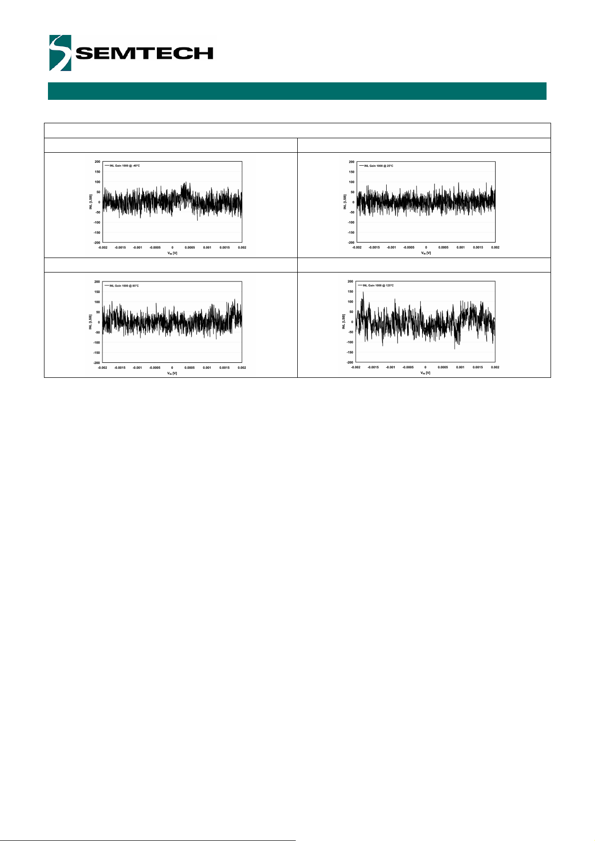
SX8724
ZoomingADC™ for Pressure and Temperature Sensing
ADVANCED COMMUNICATIONS & SENSING
-40 °C 25 °C
Gain 1000
85 °C 125 °C
V1.23 © 2009 Semtech Corp. www.semtech.com
42
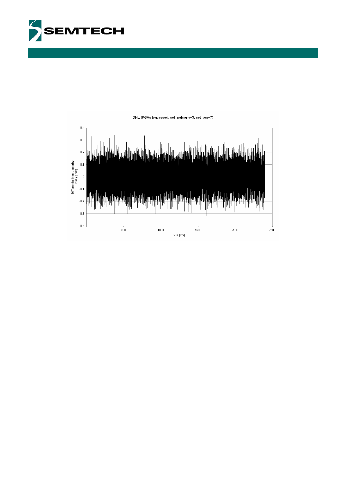
SX8724
ZoomingADC™ for Pressure and Temperature Sensing
ADVANCED COMMUNICATIONS & SENSING
Differential Non-Linearity
The differential non-linearity is generated by the ADC. The PGA does not add differential non-linearity. Figure
23 shows the differential non-linearity.
Figure 23 - Differential Non-Linearity of the ADC Converter
V1.23 © 2009 Semtech Corp. www.semtech.com
43

SX8724
ZoomingADC™ for Pressure and Temperature Sensing
ADVANCED COMMUNICATIONS & SENSING
Noise
Ideally, a constant input voltage VIN should result in a constant output code. However, because of circuit noise,
the output code may vary for a fixed input voltage. Thus, a statistical analysis on the output code of 1200
conversions for a constant input voltage was performed to derive the equivalent noise levels of PGA1, PGA2,
and PGA3. The extracted rms output noise of PGA1, 2, and 3 are given in Table 33: standard output deviation
and output rms noise voltage. Figure 24 shows the distribution for the ADC alone (PGA1, 2, and 3 bypassed).
Quantization noise is dominant in this case, and, thus, the ADC thermal noise is below 16 bits.
The simple noise model of Figure 25 is used to estimate the equivalent input referred rms noise V
acquisition chain in the model of Figure 26. This is given by the relationship:
GD
2
V
where VN1, VN2, and VN3 are the output rms noise figures of Table 33, GD1, GD2, and GD3 are the PGA gains of
stages 1 to 3 respectively. As shown in this equation, noise can be reduced by increasing OSR and N
(increases the ADC averaging effect, but reduces noise).
Parameter PGA1 PGA2 PGA3
Standard deviation at ADC
output (LSB)
Output rms noise (µV) 205 (VN1) 340 (VN2) 365 (VN3)
=
INN
,
of the
N,IN
2
V
1
1
V
+
⋅
( )
0.85 1.4 1.5
2
2
+
GDGD
21
NOSR
⋅
ELCONV
Equation 25
V
NNN
3
⋅⋅
2
GDGDGD
321
(V2rms)
ELCONV
Table 33 - PGA Noise Measurements (n = 16 bits, OSR = 512, N
ELCONV
= 2, V
REF
= 5 V)
V1.23 © 2009 Semtech Corp. www.semtech.com
44

SX8724
ZoomingADC™ for Pressure and Temperature Sensing
ADVANCED COMMUNICATIONS & SENSING
80
60
40
Occurences
20
[% of total samples]
0
-5 -4 -3 -2 -1 0 1 2 3 4 5
Output Code Deviation From Mean Value [LSB]
Figure 24 - ADC Noise (PGA1, 2 & 3 Bypassed, OSR = 512, N
PGA1 PGA2 PGA3
V
N1
V
N2
V
N3
GD1 GD2 GD3
ELCONV
f
s
ADC
= 2)
Figure 25 - Simple Noise Model for PGAs and ADC
f
PGA1 PGA2 PGA3
V
N,IN
V
N1
V
N2
V
N3
GD1 GD2 GD3
s
ADC
Figure 26 - Total Input Referred Noise
As an example, consider the system where: GD2 = 10 (GD1 = 1; PGA3 bypassed), OSR = 512, N
V
= 5 V. In this case, the noise contribution VN1 of PGA1 is dominant over that of PGA2. Using Equation 25,
REF
we get: V
= 6.4 µV (rms) at the input of the acquisition chain, or, equivalently, 0.85 LSB at the output of the
N,IN
ELCONV
= 2,
ADC. Considering 0.2 V (rms) maximum signal amplitude, the signal-to-noise ratio is 90dB.
Noise can also be reduced by implementing a software filter. By making an average on a number of subsequent
measurements, the apparent noise is reduced the square root of the number of measurement used to make the
average.
V1.23 © 2009 Semtech Corp. www.semtech.com
45
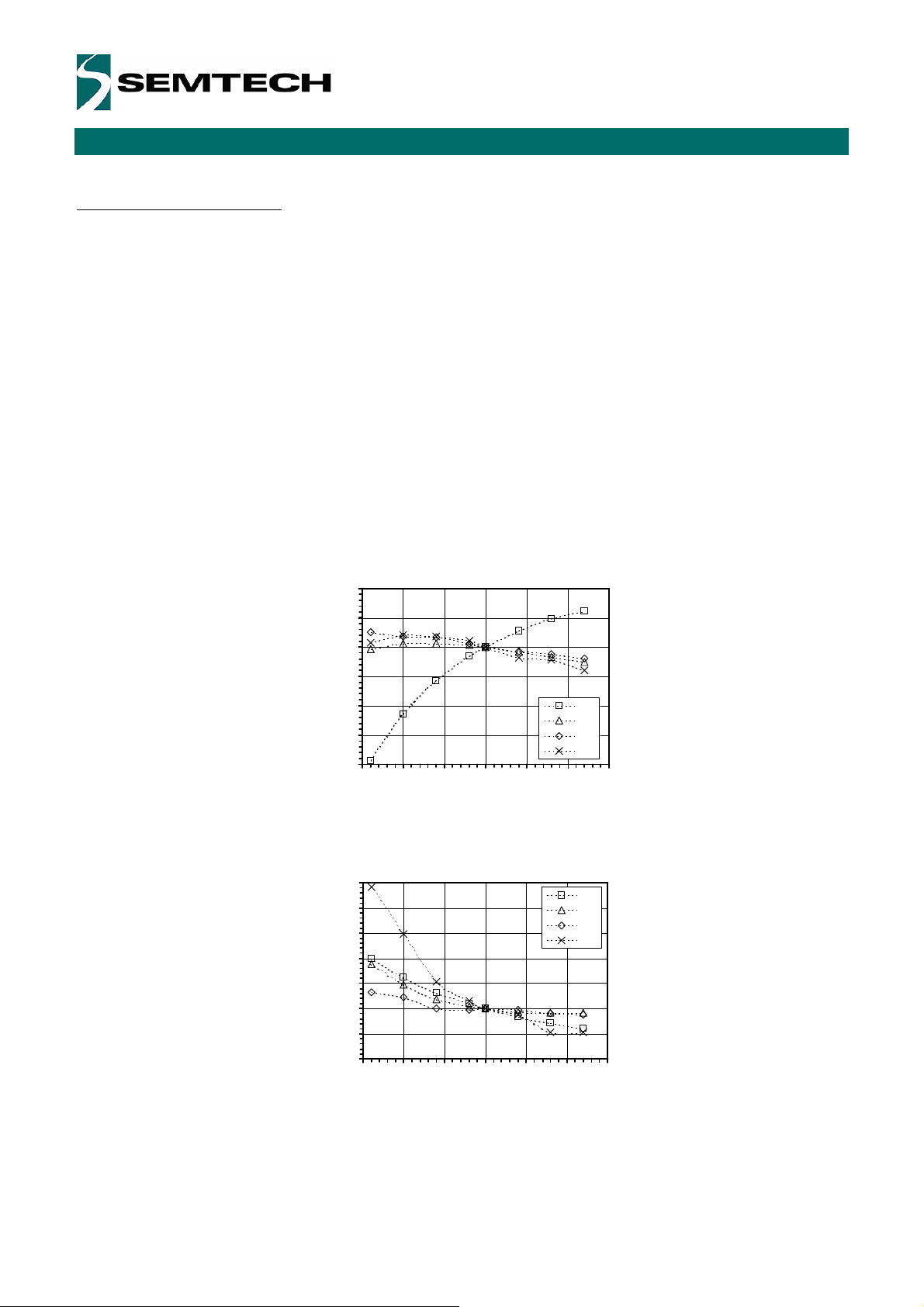
SX8724
ZoomingADC™ for Pressure and Temperature Sensing
ADVANCED COMMUNICATIONS & SENSING
Gain Error and Offset Error
Gain error is defined as the amount of deviation between the ideal transfer function (theoretical Equation 18)
and the measured transfer function (with the offset error removed).
The actual gain of the different stages can vary depending on the fabrication tolerances of the different
elements. Although these tolerances are specified to a maximum of ±3%, they will be most of the time around
±0.5%. Moreover, the tolerances between the different stages are not correlated and the probability to get the
maximal error in the same direction in all stages is very low. Finally, these gain errors can be calibrated by the
software at the same time with the gain errors of the sensor for instance.
Figure 27 shows gain error drift vs. temperature for different PGA gains. The curves are expressed in % of FullScale Range (FSR) normalized to 25°C.
Offset error is defined as the output code error for a zero volt input (ideally, output code = 0). The offset of the
ADC and the PGA1 stage are completely suppressed if NELCONV > 1.
The measured offset drift vs. temperature curves for different PGA gains are depicted in Figure 28. The output
offset error, expressed in LSB for 16-bit setting, is normalized to 25°C. Notice that if the ADC is us ed alone, the
output offset error is below ±1 LSB and has no drift.
NORMALIZED TO 25°C
0.2
0.1
0.0
-0.1
-0.2
-0.3
Gain Error [% of FSR]
-0.4
-50 -25 0 25 50 75 100
Temperature [°C]
1
5
20
100
Figure 27 - Gain Error vs. Temperature for Different PGA Gains
NORMALIZED TO 25°C
100
80
60
40
20
0
-20
Output Offset Error [LSB]
-40
-50 -25 0 25 50 75 100
Temperature [°C]
1
5
20
100
Figure 28 - Offset Error vs. Temperature for Different PGA Gains
V1.23 © 2009 Semtech Corp. www.semtech.com
46

SX8724
ZoomingADC™ for Pressure and Temperature Sensing
ADVANCED COMMUNICATIONS & SENSING
Power Consumption
Figure 29 plots the variation of quiescent current consumption with supply voltage VDD, as well as the
distribution between the 3 PGA stages and the ADC (see Table 34). As shown in Figure 30, if lower sampling
frequency is used, the quiescent current consumption can be lowered by reducing the bias currents of the PGAs
and the ADC with registers IB_AMP_PGA [1:0] and IB_AMP_ADC [1:0]. (In Figure 30, IB_AMP_PGA/ADC[1:0]
= '11', '10', '00' for fS = 500, 250, 62.5 kHz respectively.)
Quiescent current consumption vs. temperature is depicted in Figure 31, showing a relative increase of nearly
40% between -45 and +85°C.
Figure 29 - Quiescent Current Consumption vs. Supply Voltage
Figure 30 - Quiescent Current Consumption vs. Supply Voltage for Different Sampling Frequencies
V1.23 © 2009 Semtech Corp. www.semtech.com
47

SX8724
ZoomingADC™ for Pressure and Temperature Sensing
ADVANCED COMMUNICATIONS & SENSING
Figure 31 - Absolute Change in Quiescent Current Consumption vs. Temperature
Figure 32 - Relative Change in Quiescent Current Consumption vs. Temperature
Supply Back Bone ADC PGA1 PGA2 PGA3 TOTAL Unit
VDD = 5 V 142 127 96 86 97 548
VDD = 3.3 V 98 105 87 73 96 459
VDD = 2.5 V 99 105 87 71 91 453
µA
Table 34 - Typical Quiescent Current Distributions in Acquisition Chain (n = 16 bits, fS = 250 kHz)
V1.23 © 2009 Semtech Corp. www.semtech.com
48

SX8724
ZoomingADC™ for Pressure and Temperature Sensing
ADVANCED COMMUNICATIONS & SENSING
PCB Layout Considerations
PCB layout considerations to be taken when using the SX8724 are relatively simple to get the highest
performances out of the ZoomingADC. The most important to achieve good performances out the ZoomingADC
is to have a good voltage reference. The SX8724 has already an internal reference that is good enough to get
the best performances with a minimal amount of external components, but, in case an external reference is
needed this one must be as clean as possible in order to get the desired performance. Separating the digital
from the analog lines will be also a good choice to reduce the noise induced by the digital lines. It is also
advised to have separated ground planes for digital and analog signals with the shortest return path, as well as
making the power supply lines as wider as possible and to have good decoupling capacitors.
How to Evaluate
For evaluation purposes XE8000EV121 evaluation kit can be ordered. This kit connects to any PC using a USB
port. The “SX87xx Evaluation Tools” software gives the user the ability to control the SX8724 registers as well
as getting the raw data from the ZoomingADC and displaying it on the “Graphical User interface”. For more
information please look at SEMTECH web site (http://www.semtech.com).
V1.23 © 2009 Semtech Corp. www.semtech.com
49

SX8724
ZoomingADC™ for Pressure and Temperature Sensing
ADVANCED COMMUNICATIONS & SENSING
Package Outline Drawing: MLPQ-16 4x4
V1.23 © 2009 Semtech Corp. www.semtech.com
50

SX8724
ZoomingADC™ for Pressure and Temperature Sensing
ADVANCED COMMUNICATIONS & SENSING
Land Pattern Drawing: MLPQ-16 4x4
V1.23 © 2009 Semtech Corp. www.semtech.com
51

SX8724
ZoomingADC™ for Pressure and Temperature Sensing
ADVANCED COMMUNICATIONS & SENSING
Tape and Reel Specification
MLP/QFN (0.70mm - 1.00mm package thickness)
1. Single Sprocket holes
2. Tolerances for Ao & Bo are +/- 0.20mm
3. Tolerances for Ko is +/- 0.10mm
4. Tolerance for Pocket Pitch is +/- 0.10mm
5. Tolerance for Tape width is +/-0.30mm
6. Trailer and Leader Length are minimum required length
7. Package Orientation and Feed Direction
8. Tape and Reel Dimensions
carrier tape (mm) Reel
Pkg size
2.0x2.0 8 4 2.25 2.25 1.00 7 8.4 160 400 3000
2.3x2.3 12 8 2.60 2.60 1.00 13 12.4 400 400 3000
3x3 12 8 3.30 3.30 1.10 13 12.4 400 400 3000
4x4 12 8 4.35 4.35 1.10 7/13 12.4 400 400 1000/3000
4x3 12 8 3.30 4.30 1.10 13 12.4 400 400 3000
5x5 12 8 5.25 5.25 1.10 7/13 12.4 200/400 400 500/3000
6x6 16 12 6.30 6.30 1.10 13 16.4 400 400 3000
6x5 12 8 5.30 6.30 1.10 13 12.4 400 400 3000
7x7 16 12 7.30 7.30 1.10 13 16.4 400 400 3000
9X9 16 12 9.30 9.30 1.10 13 16.4 400 400 3000
10x10 24 16 10.30 10.30 1.10 13 24.4 400 400 3000
11x11 24 16 11.40 11.40 1.20 13 24.4 400 400 3000
V1.23 © 2009 Semtech Corp. www.semtech.com
52
Tape
Width
(W)
Pocket
Pitch
(P)
Ao Bo Ko
Reel
Size
(in)
Reel
Width
(mm)
Trailer
Length
(mm)
Leader
Length
(mm)
QTY per
Reel

SX8724
All rights reserved. Reproduction in whole or in part is prohibited without the prior written consent of the copyright owner.
presented in this document does not form part of any quotation or contract, is believed to be accurate and
liability will be accepted by the publisher for any consequence of its use.
ectual property rights.
r for any failure or unexpected operation resulting from misuse,
neglect improper installation, repair or improper handling or unusual physical or electrical stress including, but not limited to,
SEMTECH PRODUCTS ARE NOT DESIGNED, INTENDED, AUTHORIZED OR WARRANTED TO BE SUITABLE FOR
SUPPORT APPLICATIONS, DEVICES OR SYSTEMS OR OTHER CRITICAL APPLICATIONS. INCLUSION
PLICATIONS IS UNDERSTOOD TO BE UNDERTAKEN SOLELY AT THE
CUSTOMER’S OWN RISK. Should a customer purchase or use Semtech products for any such unauthorized application,
affiliates, and distributors harmless
against all claims, costs damages and attorney fees which could arise.
ZoomingADC™ for Pressure and Temperature Sensing
ADVANCED COMMUNICATIONS & SENSING
© Semtech 2009
The information
reliable and may be changed without notice. No
Publication thereof does not convey nor imply any license under patent or other industrial or intell
Semtech assumes no responsibility or liability whatsoeve
exposure to parameters beyond the specified maximum ratings or operation outside the specified range.
USE IN LIFEOF SEMTECH PRODUCTS IN SUCH AP
the customer shall indemnify and hold Semtech and its officers, employees, subsidiaries,
Contact Information
Semtech Corporation
Advanced Communication and Sensing Products Division
200 Flynn Road, Camarillo, CA 93012
Phone (805) 498-2111 Fax : (805) 498-3804
V1.23 © 2009 Semtech Corp. www.semtech.com
53

 Loading...