


SX8652
Touch
Screen
Interface
SX8652
VDD
X+/BR
Y+/TR
X-/TL
Y-/BL
DIN
NIRQ
SCLK
DOUT
GND
Control
SPI
Digital
Filter
ref+
ref-
ADCin out
OSC
POR
Vref
NCS
AUX/WIPER
VDD
To the
Host
To the
touch
screen
NRST (DFN only)
15kV ESD Low Power 4-Wire / 5-Wire Resistive
Touchscreen Controller with SPI Interface
ADVANCED COMMUNICATIONS & SENSING
-----4
GENERAL DESCRIPTION
The SX8652 is a very low power, high reliability controller
for 4-wire and 5-wire resistive touch screens used in PDAs,
portable instruments and point-of-sales terminal
applications. It features a wide input supply range from
1.65V to 3.7V and low power modes to preserve current
when the screen is unintentionally touched.
To compute touch screen X-Y coordinates and touch
pressure with precision, a low power 12-bit analog-digital
converter is activated with the possibility to enable on-chip
data averaging processing algorithms to reduce host activity
and suppress system noise.
The touch screen controller inputs have been specially
designed to provide robust on-chip ESD protection of up to
±15kV in both HBM and Contact Discharge, and eliminates
the need for external protection devices. The SX8652 is
controlled by a high speed SPI™ serial interface.
The SX8652 is available in a 4.0 mm x 3.0 mm 14-DFN
package and a 1.5 mm x 2.0 mm wafer level chip scale
package (WLCSP) for space conscience applications.
APPLICATIONS
DSC, DVR, Cell Phones
PDA, Pagers
Point-of-Sales Terminals
Touch-Screen Monitors
ORDERING INFORMATION
KEY PRODUCT FEATURES
Extremely Low Power Consumption: 23uA@1.8V 8kSPS
Superior On-chip ESD Protection
±15kV HBM (X+,X-,Y+,Y-)
±2kV CDM
±25kV Air Gap Discharge
±15kV Contact Discharge
±300V MM
Single 1.65V to 3.7V Supply/Reference
4-Wire or 5-Wire Resistive Touch Screen Interface
Integrated Preprocessing Block to Reduce Host Loading
and Bus Activity
Four User Programmable Operation Modes provides
Flexibility to address Different Application Needs
Manual, Automatic, Pen Detect, Pen Trigger
Low Noise Ratiometric Conversion
Precision, High Speed 12-bit SAR ADC Operating At 74k
SPS
Throughput: 5000 (X-Y) coordinates/second (c/s) with 7Sample Averaging
Low Power Shut-Down Mode < 1uA
SPI™ Serial Interface
Touch Pressure Measurement (4-Wire)
Auxiliary Input (4-Wire) For Alternate ADC Input or Start
of Conversion Trigger
Hardware & Software reset
-40°C to +85°C operation
DATASHEET
Part Number Package
SX8652ICSTRT
SX8652IWLTRT
1. 3000 Units / reel
Revision V1.7/October 2010
©2010 Semtech Corp.
1
1
(Dimension in mm)
12 - Ball WLCSP
14 - Lead DFN
(1.5x2.0)
(4.0x 3.0)
Marking
FG97
FG97
Page 1
Pb-Free, Halogen Free, RoHS/WEEE compliant product
Windows CE 6.0, Linux Driver Support Available
Packages: 14-LD (4.0 mm x 3.0 mm) DFN
12-Ball (1.5 mm x 2.0 mm) WLCSP
www.semtech.com

SX8652
ADVANCED COMMUNICATIONS & SENSING
DATASHEET
Table of contents
Section Page
1. General Description................................................................................................................................................. 4
1.1. DFN Pinout Diagram and Marking Information (Top View).............................................................................. 4
1.2. WLCSP Pinout Diagram and Marking Information (Top View) ........................................................................ 4
1.3. Pin Description................................................................................................................................................. 5
1.4. Simplified Block Diagram................................................................................................................................. 5
2. Electrical Characteristics ......................................................................................................................................... 6
2.1. Absolute Maximum Ratings ............................................................................................................................. 6
2.2. Recommended Operating Conditions.............................................................................................................. 6
2.3. Thermal Characteristics................................................................................................................................... 6
2.4. Electrical Specifications ................................................................................................................................... 7
2.5. Host Interface Specifications ........................................................................................................................... 9
2.6. Host Interface Timing Waveforms.................................................................................................................... 9
3. Functional Description ........................................................................................................................................... 10
3.1. General Introduction ..................................................................................................................................... 10
3.2. Device Interface and ESD protection............................................................................................................. 11
3.2.1. Touchscreen interface............................................................................................................................. 11
3.2.2. Host Interface and Control Pins .............................................................................................................. 11
4. 4-wire Touch Screen Detailed Description ............................................................................................................ 12
4.1. Touch Screen Operation................................................................................................................................ 12
4.2. Coordinates Measurement............................................................................................................................. 12
4.3. Pressure Measurement.................................................................................................................................. 13
4.4. Pen Detection ................................................................................................................................................ 13
5. 5-wire Touch Screen Detailed Description ............................................................................................................ 14
5.1. Touch Screen Operation................................................................................................................................ 14
5.2. Coordinates Measurement............................................................................................................................. 14
5.3. Pen Detection ................................................................................................................................................ 14
6. Data Processing .................................................................................................................................................... 15
7. Power-Up, Reset ................................................................................................................................................... 15
8. Modes of Operation ............................................................................................................................................... 15
8.1. MANual Mode ................................................................................................................................................ 16
8.2. AUTOmatic mode .......................................................................................................................................... 16
8.3. PENDET Mode .............................................................................................................................................. 17
8.4. PENTRIG Mode............................................................................................................................................. 17
9. Host Interface ........................................................................................................................................................ 19
9.1. SPI Read/Write Registers.............................................................................................................................. 19
9.2. SPI Reading Channel Data............................................................................................................................ 19
9.3. SPI Host Commands ..................................................................................................................................... 20
9.4. SPI implementation and multiple Read/Write ................................................................................................ 20
9.5. Invalid Qualified Data..................................................................................................................................... 21
Revision V1.7/October 2010
©2010 Semtech Corp.
Page 2
www.semtech.com

SX8652
ADVANCED COMMUNICATIONS & SENSING
DATASHEET
Table of contents
Section Page
9.6. Register Map................................................................................................................................................. 22
9.7. SX8652 register ............................................................................................................................................ 23
10. Application Information ......................................................................................................................................... 24
10.1. Acquisition Setup ........................................................................................................................................... 24
10.2. Channel Selection.......................................................................................................................................... 24
10.3. Noise Reduction............................................................................................................................................. 24
10.3.1. POWDLY................................................................................................................................................. 24
10.3.2. SETDLY .................................................................................................................................................. 25
10.4. AUX Input - 4-wire touchscreen only ............................................................................................................. 25
10.5. Interrupt Generation....................................................................................................................................... 25
10.6. Coordinate Throughput Rate ......................................................................................................................... 25
10.6.1. SPI Communication Time ....................................................................................................................... 25
10.6.2. Conversion Time..................................................................................................................................... 26
10.7. ESD event...................................................................................................................................................... 26
11. Packaging Information........................................................................................................................................... 27
11.1. DFN Package................................................................................................................................................. 27
11.2. WLCSP Package ........................................................................................................................................... 28
Revision V1.7/October 2010
©2010 Semtech Corp.
Page 3
www.semtech.com

SX8652
1
2
3
4
5
6
14
13
12
11
10
9
AUX/
WIPER
(NC)
VDD
X+/BR
Y+/TR
X-/TL
NRST
DIN
NCS
NIRQ
DOUT
Y-/BL
15
7
GND
8
SCLK
PIN
1
IDENTIFIER
FG97
YYWW
XXXXX
#
A
NIRQ SCLKDOUT
B C D
3
2
1
VDD NCS GNDDIN
X+/BR Y+/TR Y-/BLX-/TL
AUX/WIPER
FG97
YYWW
XXXXXX
BALL A1 IDENTIFIER
15kV ESD Low Power 4-Wire / 5-Wire Resistive
Touchscreen Controller with SPI Interface
ADVANCED COMMUNICATIONS & SENSING
1. General Description
1.1. DFN Pinout Diagram and Marking Information (Top View)
DATASHEET
Figure 1. SX8652 DFN Top View, Pad on Bottom Side
YYWW: date code
XXXXX: Lot Number
1.2. WLCSP Pinout Diagram and Marking Information (Top View)
YYWW: date code
XXXXX: Lot Number
Figure 2. SX8652 WLCSP Top View, Solder Bumps on Bottom Side
Revision V1.7/October 2010
©2010 Semtech Corp.
Page 4
www.semtech.com
SX8652
Touch
Screen
Interface
SX8652
VDD
X+/BR
Y+/TR
X-/TL
Y-/BL
DIN
NIRQ
SCLK
DOUT
GND
Control
SPI
Digital
Filter
ref+
ref-
ADCin out
OSC
POR
Vref
NCS
AUX/WIPER
VDD
To the
Host
To the
touch
screen
NRST (DFN only)
15kV ESD Low Power 4-Wire / 5-Wire Resistive
Touchscreen Controller with SPI Interface
ADVANCED COMMUNICATIONS & SENSING
DATASHEET
1.3. Pin Description
Pin Number #Name Type Description
DFN WLCSP
1 A1 AUX/WIPER Digital Input /
Analog Input
2 A2 VDD Power Input Input power supply, connect to a 0.1uF capacitor to GND
3 A3 X+/BR Analog IO X+ Right electrode (4-wire) / Bottom Right (5-wire) channel
4 B3 Y+/TR Analog IO Y+ Top electrode (4-wire) /Top Right (5-wire) channel
5 C3 X-/TL Analog IO X- Left electrode (4-wire) /Top Left (5-wire) channel
6 D3 Y-/BL Analog IO Y- Bottom electrode (4-wire) /Bottom Left (5-wire) channel
7 D2 GND Ground Ground
8 D1 SCLK Digital Input SPI Serial Clock Input
9 C2 DIN Digital Output SPI Serial Data Input
10 C1 DOUT Digital Output SPI Serial Data Output
11 B1 NIRQ Digital Output, open drain Interrupt Request Output, Active low, Need external pull-up
12 B2 NCS Digital Input SPI Chip Select Input, Active low
13 - NRST Digital Input DFN package only, Reset Input, Active low, Internal pull-up resistor
14 - (NC) Not Connected
15 - GND Power input Backside Ground
Conversion Synchronization (4-wire) or
Analog Auxiliary Input (4-wire) / Wiper Input (5-wire)
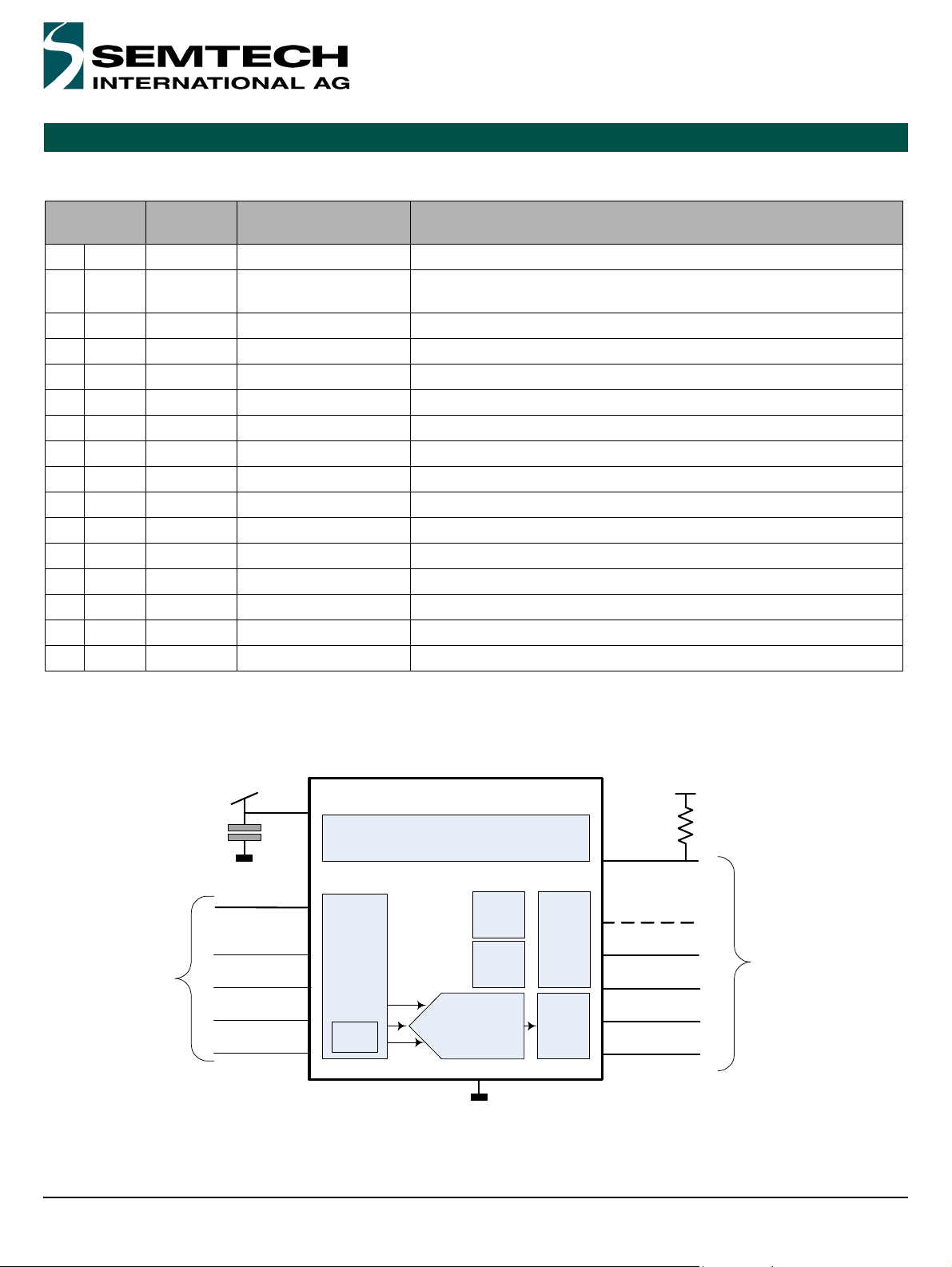
1.4. Simplified Block Diagram
The SX8652 simplified block diagram is shown in Figure 3.
Revision V1.7/October 2010
©2010 Semtech Corp.
Figure 3. Simplified block diagram of the SX8652
Table 1. Pin description
Page 5
www.semtech.com

SX8652
15kV ESD Low Power 4-Wire / 5-Wire Resistive
Touchscreen Controller with SPI Interface
ADVANCED COMMUNICATIONS & SENSING
DATASHEET
2. Electrical Characteristics
2.1. Absolute Maximum Ratings
Stresses above the values listed in “Absolute Maximum Ratings” may cause permanent damage to the device.
This is a stress rating only and functional operation of the device at these, or any other conditions beyond the “Recommended Operating
Conditions”, is not implied. Exposure to absolute maximum rating conditions for extended periods may affect device reliability
Parameter Symbol Min. Max. Unit
Supply Voltage V
Input voltage (non-supply pins) V
Input current (non-supply pins) I
Operating Junction Temperature T
Reflow temperature T
Storage temperature T
High ESD pins: X+/BR, X-/TL,
ESD HBM
(Human Body Model)
Y+/TR, Y-/BL, Aux/Wiper
All pins except high ESD pins ESD
DDABS
ESD
IN
IN
JCT
RE
STOR
HBM1
HBM2
-0.5 3.9 V
-0.5 3.9 V
10 mA
125 °C
260 °C
-50 150 °C
(i)
± 15
(ii)
± 8
± 2 kV
.
kV
kV
ESD (Contact Discharge) High ESD pins: X+/BR, X-/TL,
Y+/TR, Y-/BL, Aux/Wiper
Latchup
(iii)
ESD
Table 2. Absolute Maximum Ratings
(i) Tested to TLP (10A)
(ii) Tested to JEDEC standard JESD22-A114
(iii) Tested to JEDEC standard JESD78
2.2. Recommended Operating Conditions
Parameter
Supply Voltage V
Ambient Temperature Range T
Table 3. Recommended Operating Conditions
Symbol Min. Max Unit
2.3. Thermal Characteristics
Parameter
Thermal Resistance with DFN package - Junction to Ambient
Thermal Resistance with WLCSP package - Junction to Ambient
(iii)
(iii)
Symbol Min. Max Unit
CD
I
LU
DD
A
θ
JA
θ
JA
± 15 kV
± 100 mA
1.65V 3.7 V
-40 85 °C
39 °C/W
65 °C/W
Table 4. Thermal Characteristics
(
iii) θJA is calculated from a package in still air, mounted to 3" x 4.5", 4 layer FR4 PCB with thermal vias under exposed pad (if applicable)
per JESD51 standards.
Revision V1.7/October 2010
©2010 Semtech Corp.
Page 6
www.semtech.com

SX8652
15kV ESD Low Power 4-Wire / 5-Wire Resistive
Touchscreen Controller with SPI Interface
ADVANCED COMMUNICATIONS & SENSING
2.4. Electrical Specifications
All values are valid within the recommended operating conditions unless otherwise specified.
Parameter
Current consumption
Mode = MANUAL I
Mode = PENDET I
Mode =PENTRIG I
Mode=AUTO I
Symbol Conditions Min. Typ Max Unit
pwd
pndt
pntr
auto
Converter stopped, pen
detection off, SPI listening,
OSC stopped
Converter stopped, pen
detection activated, device
generates interrupt upon
detection, SPI listening, OSC
stopped
Converter stopped, pen
detection activated, device
starts conversion upon pen
detection. SPI listening, OSC
stopped
Converter stopped, pen
detection off, SPI listening,
OSC on, timer on
DATASHEET
0.4 1 uA
0.4 1 uA
0.4 1 uA
1.5 uA
Operation @8kSPS, VDD=1.8V I
Operation @42kSPS, VDD=3.3V I
Digital I/O
High-level input voltage V
Low-level input voltage V
Hysteresis
Output Logic High V
Output Logic Low V
Input leakage current L
High ESD Input - Output
capacitance
Input - Output capacitance C
opl
oph
IH
IL
V
HysLow
V
HysHigh
OH
OL
I
C
,C
X+/BR
,C
Y+/TR
C
AUX
NRST , CNIRQ
,C
NCS ,CDIN
C
DOUT, CSCLK
X-/TL
, C
Y-/BL,
,
23 50 uA
105 140 uA
0.8V
DD
VSS-0.3 0.2V
VDD > 2V 0.05 V
VDD < 2V 0.1 V
IOH>-2mA 0.8V
IOL<2mA 0 0.4 V
CMOS input ±1 uA
DD
50 pF
VDD+0.2 V
DD
DD
5 pF
DD
V
V
V
Revision V1.7/October 2010
©2010 Semtech Corp.
Table 5. Electrical Specifications
Page 7
www.semtech.com

SX8652
15kV ESD Low Power 4-Wire / 5-Wire Resistive
Touchscreen Controller with SPI Interface
ADVANCED COMMUNICATIONS & SENSING
Parameter
Startup
Power-up time t
ADC
Resolution A
Offset A
Gain error A
Differential Non Linearity A
Integral Non Linearity A
Symbol Conditions Min. Typ Max Unit
por
res
off
ge
dnl
inl
Time between rising edge VDD
and rising NIRQ
At full scale 0.5 LSB
DATASHEET
1 ms
12 bits
±1 LSB
±1 LSB
±1.5 LSB
Resistors
X+, X-, Y+, Y- resistance R
Pen detect resistance R
chn
PNDT_00
R
PNDT_01
R
PNDT_10
R
PNDT_11
Touch Pad Biasing Resistance 5 Ohm
R
= 0 100 kOhm
PNDT
R
= 1 200 kOhm
PNDT
R
= 2 50 kOhm
PNDT
R
= 3 25 kOhm
PNDT
External components recommendations
Capacitor between VDD, GND C
vdd
Type 0402, tolerance +/-50% 0.1 uF
Table 5. Electrical Specifications
Revision V1.7/October 2010
©2010 Semtech Corp.
Page 8
www.semtech.com

SX8652
tCKH
tDS
tDH
tCSS tCKL
tDCD
tDOD
tCSW
tCSI
tCCZ
CSN
SCLK
DIN
DOUT
D11
VOL
VOH
50%VDD
50%VDD
50%VDD
15kV ESD Low Power 4-Wire / 5-Wire Resistive
Touchscreen Controller with SPI Interface
ADVANCED COMMUNICATIONS & SENSING
DATASHEET
2.5. Host Interface Specifications
Parameter Symbol Condition Min Typ Max Unit
SPI TIMING SPECIFICATIONS
SCLK
Clock Frequency
Duty Cycle
NCS edge to first SCLK “↑” T
NCS edge to DOUT Low T
SCLK High Pulse Width T
SCLK Low Pulse Width T
Data Setup Time T
Data Valid to SCLK Hold Time T
Data Output Delay after SCLK “↓” T
NCS “↑” to SCLK Ignored T
(i)
f
SCLK
duty
CSS
DCD
CKH
CKL
DS
DH
DOD
CSI
40
50
80
80
40
70
50
5000
60
100
70
kHz
%
ns
NCS “↑” to DOUT Hi-Z state T
NCS Hold Time T
(i) All timing specifications refer to voltage levels (50% VDD, VOH, VOL) defined in Table 6 unless otherwise mentioned.
CCZ
CSW
150
Table 6. Host Interface Specifications
2.6. Host Interface Timing Waveforms
Figure 4. SPI Timing Waveform
90
Revision V1.7/October 2010
©2010 Semtech Corp.
Page 9
www.semtech.com

SX8652
Touch
Screen
Interface
SX8652
VDD
X+/BR
Y+/TR
X-/TL
Y-/BL
DIN
NIRQ
SCLK
DOUT
GND
Control
SPI
Digital
Filter
ref+
ref-
ADCin out
OSC
POR
Vref
NCS
AUX/WIPER
VDD
NRST (DFN only)
HOST
INT
DIO
CS
SCLK
MISO
MOSI
SPI
Interface
4-wire touchscreen
Touch
Screen
Interface
SX8653
VDD
X+/BR
Y+/TR
X-/TL
Y-/BL
DIN
NIRQ
SCLK
DOUT
GND
Control
SPI
Digital
Filter
ref+
ref-
ADCin out
OSC
POR
Vref
NCS
AUX/WIPER
VDD
NRST (DFN only)
HOST
INT
DIO
CS
SCLK
MISO
MOSI
SPI
Interface
5-wire touchscreen
15kV ESD Low Power 4-Wire / 5-Wire Resistive
Touchscreen Controller with SPI Interface
ADVANCED COMMUNICATIONS & SENSING
DATASHEET
3. Functional Description
3.1. General Introduction
This section provides an overview of the SX8652 architecture, device pinout and a typical application.
The SX8652 is designed for 4-wire and 5-wire resistive touch screen applications. The touch screen or touch panel is the
resistive sensor and can be activated by either a finger or stylus. When the top layer is pressed, it makes contact with the
bottom sheet and the touch location can be measured.
As shown in Figure 5 with a 4-wire panel, the touch screen coordinates and touch pressure are converted into SPI format
by the SX8652 for transfer to the host. The auxiliary input can be used to convert with 12-bit resolution any analog input in
the supply range. It can also serves as an external synchronisation input to trig the touchscreen acquisition as described in
the Application Information section.
Figure 5. SX8652 with a 4-wire touch screen
A 5-wire touchscreen application is shown in Figure 6. The 5-wire top sheet acts as a voltage measuring probe. The
measurement accuracy is not affected by damage on this sheet and consequently the reliability is improved but the touch
pressure can not be calculated.
www.semtech.com
Revision V1.7/October 2010
©2010 Semtech Corp.
Figure 6. SX8652 with a 5-wire touch screen
Page 10

SX8652
T o uch
S c re e n
D riv e rs
In te rfac e
R
ch n
A
D
C
C o n trol
D a ta Pro cess in g
X + /B R
X -/TL
Y + /T R
Y -/B L
A U X /
W ip e r
M U X
R
ch n
R
ch n
R
ch n
P o w er
M an ag e m en t
V D D
G N D
N R S T
N IR Q
S P I
NCS
SCLK
DOUT
DIN
15kV ESD Low Power 4-Wire / 5-Wire Resistive
Touchscreen Controller with SPI Interface
ADVANCED COMMUNICATIONS & SENSING
DATASHEET
3.2. Device Interface and ESD protection
The touch screen controller inputs have been specially designed to provide robust on-chip ESD protection of up to ±15kV
in both HBM and Contact Discharge.
3.2.1. Touchscreen interface
The X+/BR, X-/TL, Y+/TR,Y-/BL, AUX/WIPER are the pins dedicated for the touchscreen interface. It provides the voltage
sequence in order to obtain the coordinates and pressure measurement.
The five pins are connected to BR, TL, TR, BL, WIPER on a 5-wire touchscreen. They are the electrodes on the 4 corners
of the bottom layer of the touchscreen plus the electrode on the top layer.
On a 4-wire touchscreen, only 4 electrodes are used: X+,X-,Y+,Y-. The AUX pin is not needed and therefore can be used
to convert an analog signal (range GND - VDD) into 12-bit digital value. The touchscreen interface pins are the most
exposed pins for an ESD event.
As shown in Figure 7, theses pins have internal ESD protection to GROUND and VDD.
3.2.2. Host Interface and Control Pins
The SX8652 is a slave device configured via the SPI interface.
NIRQ provides an interrupt to the host processor when a pen is detected or when channel data is available. The NIRQ pin
is an active low, open drain output to facilitate interfacing to different supply voltages and thus requires an external pull-up
resistor (1-10 kOhm).
The host can reset the chip via the SPI interface or with the dedicated pin NRST. The NRST pin is an active low input that
provides a hardware reset. An internal pull-up enables the interfacing with devices at different supply voltage.
NRST and NIRQ pins are protected to GROUND.
Revision V1.7/October 2010
©2010 Semtech Corp.
Figure 7. ESD protection
Page 11
www.semtech.com

SX8652
X-
Y+
Y-
X+
T
o
p
c
o
n
d
u
c
t
i
v
e
s
h
e
e
t
B
o
t
t
o
m
c
o
n
d
u
c
t
i
v
e
s
h
e
e
t
Y
e
l
e
c
t
r
o
d
e
s
X
e
l
e
c
t
r
o
d
e
s
Y
-
Y
+
R
y
t
o
t
Top conductive sheet before
the stylus contact
Y
-
Y
+
R
4
R
3
Top conductive sheet after
the stylus contact
Contact point
with the top
conductive
sheet
Rxtot R1 R2+=
Rytot R3 R4+=
X-
X+
R2
R1
+
-
R
T
Y-
Y+
R4
R3
Xpos
+
-
ADC
Vref
Xpos 4095
R2
R1 R2+
--------------------
⋅=
Ypos 4095
R4
R3 R4+
--------------------
⋅=
15kV ESD Low Power 4-Wire / 5-Wire Resistive
Touchscreen Controller with SPI Interface
ADVANCED COMMUNICATIONS & SENSING
DATASHEET
4. 4-wire Touch Screen Detailed Description
4.1. Touch Screen Operation
A 4-wire resistive touch screen consists of two resistive sheets separated by an insulator (Figure 4.2).
Figure 8. 4-wire Touch Screen
When a pressure is applied on the top sheet with a stylus for example, a connection with the lower sheet is made.
The contact point split the Rxtot bottom resistance in the vertical axis into two resistances
R1 and R2. In the same way, the Rytot resistance in the horizontal axis of the top sheet is
divided into two resistances R3 and R4.
The touchscreen controller imposes a voltage level on X or Y electrodes allowing the
detection of the contact position.
4.2. Coordinates Measurement
During the touch, the top and bottom touchscreen layers
are connected. The resistance between the two sheets
is RT. A current coming from the reference voltage goes
from X+ to X- to perform the X coordinate
measurement. Figure 9 shows the measurement
schematics.
Since the ADC had a high input impedance, no current
flows through RT and R3. The positive ADC input is
biased with a voltage created by the R1, R2 voltage
divider.
The conversion with the 12 bit ADC gives the X location.
Figure 9. Abscissa (X) coordinates measurement
The Y coordinate is measured in a similar fashion with the measurement setup given in Table 7.
Revision V1.7/October 2010
©2010 Semtech Corp.
Page 12
www.semtech.com

SX8652
z1 4095
R4
R1 R4 R
T
+ +
---------------------------------
⋅= z2 4095
R4 Rt+
R1 R4 R
T
+ +
---------------------------------
⋅=
R
T
Rytot
Ypos
4095
------------
z2
z1
-----
1–⋅ ⋅=
R
T
Rytot Y⋅ pos
4095
-------------------------------
4095
z1
------------
1– Rxtot 1
Xpos
4095
-------------
–⋅–⋅=
X-
X+
R2
R1
Vref
+
-
R
T
Y-
Y+
R
4
R3
R
PNDT
Sb
Rb
IRQ
Q
Q
Internal
logic
15kV ESD Low Power 4-Wire / 5-Wire Resistive
Touchscreen Controller with SPI Interface
ADVANCED COMMUNICATIONS & SENSING
DATASHEET
4.3. Pressure Measurement
The 4-wire touchscreen allows pressure measurement. The contact resistance between the two sheets are a function of
the pressure applied on the top sheet. Indeed, the a low pressure applied with the finger will create a small contact area.
With a greater pressure, the contact area will be bigger and the RT resistance smaller.
The RT contact resistance is therefore an indication of the applied pressure. RT is deducted from Z1 and Z2 measurement.
The measurement setup given in Table 7 allows to find Z1 and Z2.
Arranging Z1 and Z2 with Rxtot and Rytot allows the
computation of RT.
An alternative calculation method is using Xpos and Ypos.
Measurement Vref + Vref- ADC +
X
Y
Z1
Z2
X+ X- Y+
Y+ Y- X+
X+ Y- Y+
X+ Y- X-
Table 7. Measurement setup
4.4. Pen Detection
The pen detection circuitry is used to detect a user action on the
touchscreen. The contact between the two layers generates an interrupt or
starts an acquisition sequence.
Doing a pen detection prior to conversion avoids feeding the host with
dummy data and saves power.
If the touchscreen is powered between X+ and Y- through a resistor R
no current will flow so long as pressure is not applied to the surface (see
Figure 10).
When a pressure is applied, a current path is created and brings X+ to the
level defined by the resistive divider determined by R
R1, RT and R4.
R
should be set to the greatest value of 200 kOhm for optimal detection (see Table 15). Increasing PowDly settings
PNDT
can also improve the detection on panel with high resistance.
The pen detection will set the PENIRQ bit of the RegStat register. The PENIRQ bit will be cleared and the NIRQ will be de-
asserted as soon as the host reads the status register.
In PENDET mode, the pen detection will set NIRQ low.
Revision V1.7/October 2010
©2010 Semtech Corp.
and the sum of
PNDT
Page 13
PNDT
,
Figure 10. 4-wire pen detection circuitry
www.semtech.com

SX8652
T
L
B
L
B
o
t
t
o
m
c
o
n
d
u
c
t
i
v
e
s
h
e
e
t
T
R
B
R
T
o
p
c
o
n
d
u
c
t
i
v
e
s
h
e
e
t
W
i
p
e
r
L
i
n
e
a
r
i
s
a
t
i
o
n
p
a
t
t
e
r
n
Xpos 4095
R2
R1 R2+
--------------------
⋅=
Ypos 4095
R4
R3 R4+
--------------------
⋅=
BR
R1
Vref
+
-
AUX/
WIPER
-
R
PNDT
Sb
Rb
Q
Q
Internal
logic
Bottom
layer
Top
layer
15kV ESD Low Power 4-Wire / 5-Wire Resistive
Touchscreen Controller with SPI Interface
ADVANCED COMMUNICATIONS & SENSING
DATASHEET
5. 5-wire Touch Screen Detailed Description
5.1. Touch Screen Operation
As the 4-wire, the 5-wire resistive touch screen consists of two resistive
sheets separated by an insulator (Figure 11). The main difference is that
the 4 wires are connected on the 4 corners of the bottom conductive
sheet. They are referred as Top Left, Top Right, Bottom Left, Bottom
Right.
The fifth wire is embedded in the top sheet and is used for sensing the
electrode voltage and is referred as the wiper.
Figure 11. 5-wire touchscreen
5.2. Coordinates Measurement
When the electrodes TL is connected with BL and TR with BR, they form with the linearization pattern 2 electrodes bars
which are very similar to the X electrodes in a 4-wire touchscreen. In the same way, the association of TL with TR and BL
with BR create Y electrodes.
The four corners are therefore able to produce voltage gradients in the horizontal and vertical axis. The wiper is connected
to the high input impedance of the ADC. When a pressure is applied on the top sheet, the contact point split the bottom
sheet resistance into R1 and R2 on the X axis and R3 and R4 on the Y axis.
The X and Y position converted by the 12-bit ADC
gives the following result.
5.3. Pen Detection
The BR pin is connected to the positive pin of the reference voltage through
R
. The wiper panel is grounded at the AUX/WIPER pin to provide the
PNDT
grounding path for a screen touch event.
The BR pin is monitored to detect voltage drop. When a pressure is applied on
the top surface, a current path is created between the two layers and the
PENIRQ bit of the RegStat register will be set. R
greatest value of 200 kOhm for optimal detection (see Table 15). Increasing
PowDly settings can also improve the detection on panel with high resistance.
In PENDET mode, the pen detection will set NIRQ low.
Revision V1.7/October 2010
©2010 Semtech Corp.
should be set to the
PNDT
Page 14
Figure 12. 5-wire pen detection circuitry
www.semtech.com

SX8652
s
n
cn=
s
n
1
3
---
K
cnc
n 1–
c
n 2–
+ +( )=
s
n
1
5
---
K
cnc
n 1–
c
n 2–
c
n 3–
c
n 4–
+ + + +( )=
c
max1cmax2cacbcccmin1cmin2
≥ ≥ ≥ ≥ ≥ ≥
s
n
1
3
---
K
cacbc
c
+ +( )=
voltage
time
voltage
time
VDD
NIRQ
t
POR
VDD/2
15kV ESD Low Power 4-Wire / 5-Wire Resistive
Touchscreen Controller with SPI Interface
ADVANCED COMMUNICATIONS & SENSING
DATASHEET
6. Data Processing
The SX8652 offers 4 types of data processing which allows the user to make trade-offs between data throughput, power
consumption and noise rejection. The parameter FILT is used to select the filter order N
The sn samples from the ADC can be averaged. The processed cn 12-bit value is then send through the SPI bus.
The noise rejection will be improved with a high order to the detriment of the power consumption.
The K coefficient in Table 8 is a filter constant. Its value is K=4079/4095.
FILT N
0 1 No average
1 3 3 ADC samples are averaged
2 5 5 ADC samples are averaged
3 7 7 ADC samples are sorted and
filt
Explanation Processing
the 3 center samples are
averaged
Table 8. Filter order
as seen in Table 8.
filt
7. Power-Up, Reset
During power-up, NIRQ pin is kept low, the POR reset all
registers and states of the SX8652. The SX8652 is not
accessible and SPI communications are ignored.
As soon as NIRQ rises, the SX8652 is in manual mode with
only the SPI peripheral enabled to minimize power
consumption.
The host can reset the SX8652 by setting the NRST pin low or
via the SPI bus. Writing the code 0xDE to the register
RegSoftReset reset the circuit.
When NRST is driven LOW by the host, NIRQ will be driven low
by the SX8652. After the reset NIRQ will be released by the
SX8652.
Figure 13. Power-up, NIRQ
8. Modes of Operation
The SX8652 has four operation modes that are configured using the SPI commands as defined in Table 13 and Table 15.
These 4 modes are:
manual (command ‘MANAUTO’ and RATE=0),
automatic (command ‘MANAUTO’ and RATE>0),
pen detect (command ‘PENDET’),
pen trigger mode (command ‘PENTRG’).
Revision V1.7/October 2010
©2010 Semtech Corp.
Page 15
www.semtech.com

SX8652
15kV ESD Low Power 4-Wire / 5-Wire Resistive
Touchscreen Controller with SPI Interface
ADVANCED COMMUNICATIONS & SENSING
In the PENDET mode the pen detection is activated. The SX8652 will generate an interrupt (NIRQ) upon pen detection and
set the PENIRQ bit in the SPI status register. To quit the PENDET mode the host needs to configure the manual mode.
In the PENTRG mode the pen detection is activated and a channel conversion will start after the detection of a pen. The
SX8652 will generate an interrupt (NIRQ) upon pen detection and set the CONVIRQ bit in the SPI status register. To quit
the PENTRIG mode the host needs to configure the manual mode. The PENTRG mode offers the best compromise
between power consumption and coordinate throughput.
DATASHEET
8.1. MANual Mode
In manual mode (RATE=0), the host sequences all the actions by the SPI commands described in Table 9.
When a command is received, the SX8652 executes the associated task and waits for the next command.
Command
CONVERT(CHAN)
SELECT(CHAN)
Select and bias a channel
Wait for the programmed settling time (POWDLY)
Start conversion
Select and bias a channel
Table 9. CONVERT and SELECT command
The channel can be biased for an arbitrary amount of time by first sending a SELECT command and then a CONVERT
command once the settling time requirement is met.
The SELECT command can be omitted if the large range of POWDLY settings cover the requirements. In the latter case,
the CONVERT command alone is enough to perform an acquisition.
With CHAN=SEQ, multiple channels are sampled. This requires programming the POWDLY field in register RegCTRL0.
The selected channel will be powered during POWDLY before a conversion is started. The channel bias is automatically
removed after the conversion has completed.
Action
8.2. AUTOmatic mode
In automatic mode (RATE > 0), SX8652 start the acquisition when a touch is detected. It converts all the channels selected
with RegChnMsk and set NIRQ low when it is finished.
After the host has read the channels, if CONDIRQ=1 and the touch is detected again, the SX8652 starts a new conversion
cycle.
To not loose data, the SX8652 does not begin conversion before the host read all the channels.
We can define the time ts between the start of the conversion and the end of the channels reading by the host.
The rate programmed is achieved if ts<1/RATE otherwise the new rate is 1/ts.
When the control CONDIRQ bit (see register RegStat Table 15) is set to ‘1’ then the interrupts will only be generated if the
pen detect occurred. This result in a regular interrupt stream, as long as the host performs the read channel commands,
and the screen is touched. When the screen is not touched, interrupts does not occur.
If the control CONDIRQ bit is cleared to ‘0’, the interrupts will be always generated. In case there is no pen detected on the
screen then the coordinate data will be qualified as invalid, see section [9.5]. This result in a regular interrupt stream as
long as the host performs the read channel commands,
This working is illustrated in Figure 16.
Figure 14 shows the SPI working in automatic mode with CONDIRQ=1. After the first sentence send through the SPI to
make the initialization, traffic is reduced as only reads are required.
Revision V1.7/October 2010
©2010 Semtech Corp.
Page 16
www.semtech.com

SX8652
CS
DIN
DOUT
TOUCH
NIRQ
Read Channel Data CMD
Data from SX8652
Processing time
Time is 1/RATE
CS
DIN
DOUT
TOUCH
NIRQ
Read Channel Data CMD
Data from SX8652
Conversion time
15kV ESD Low Power 4-Wire / 5-Wire Resistive
Touchscreen Controller with SPI Interface
ADVANCED COMMUNICATIONS & SENSING
The processing time is the
necessary time for the SX8652 to
makes the pen detection, the
settling time (POWDLY) and the
conversion of the selected
channels. This time increases with
the number of channel selected
and the filter used. NIRQ interrupt
signal notifies the host when the
conversions are done.
The host just need to read the
channels data to release the
interrupt.
DATASHEET
Figure 14. SPI working in AUTO mode
8.3. PENDET Mode
The PENDET mode can be used if the host only needs to know if the screen has been touched or not and take from that
information further actions. When pen detect circuitry is triggered the interrupt signal NIRQ will be generated and the status
register bit ‘PENIRQ’ will be set. The bit is cleared by reading the status register RegStat. The PENDET working is
illustrated in Figure 16.
8.4. PENTRIG Mode
The PENTRIG mode offers the best
compromise between power consumption
and coordinate throughput.
In this mode the SX8652 will wait until a pen
is detected on the screen and then starts the
coordinate conversions. The host will be
signaled only when the screen is touched and
coordinates are available. The flowchart is
describes in Figure 16.
The coordinate rate in pen trigger mode is
determined by the speed of the host reading
the channels and the conversion times of the
channels. The host performs the minimum
number of SPI commands in this mode.
The host has to wait for the NIRQ interrupt to
make the acquisition of the data.
The SPI working is illustrated in Figure 15.
Figure 15. SPI working in PENTRIG mode
Revision V1.7/October 2010
©2010 Semtech Corp.
Page 17
www.semtech.com

SX8652
Touch Detected ?
Start channel conversion
Set interrupt
NIRQ=0
Release Interrupt
NIRQ=1
All channel
data read
All conversion
finished
yes
no
PENTRIG MODE
CONDIRQ=1 ?
Touch Detected ?
Set timer=RATE
Start timer
Start channel conversion
Set interrupt
NIRQ=0
Release Interrupt
NIRQ=1
yes
Timer expire
All channel
data read
All conversion
finished
yes
no
AUTO MODE
Touch Detected ?
Set interrupt
NIRQ=0
Release Interrupt
NIRQ=1
RegStat read
yes
no
PENDET MODE
15kV ESD Low Power 4-Wire / 5-Wire Resistive
Touchscreen Controller with SPI Interface
ADVANCED COMMUNICATIONS & SENSING
DATASHEET
Revision V1.7/October 2010
©2010 Semtech Corp.
Figure 16. AUTO, PENDET and PENTRIG Mode Flowchart
Page 18
www.semtech.com

SX8652
15kV ESD Low Power 4-Wire / 5-Wire Resistive
Touchscreen Controller with SPI Interface
ADVANCED COMMUNICATIONS & SENSING
DATASHEET
9. Host Interface
The host interfaced is composed of a SPI bus. It performs the read/ write operations on the registers and channels data.
9.1. SPI Read/Write Registers
The WRITE command allows the host to write a single or multiple registers in the SX8652. The host can read single or
multiple registers from the SX8652 by the READ command. This is defined in Table 10.
W/R command name CR(7:0) Function
7 6 5 4 3 2 1 0
WRITE(RA) 0 0 0 RA(4:0) Write register (see Table 14 for RA)
READ(RA) 0 1 0 RA(4:0) Read register (see Table 14 for RA)
Table 10. W/R commands
9.2. SPI Reading Channel Data
Five channels can be sampled by the SX8652: X, Y, Z1, Z2 and AUX. They are defined in Table 12. They can be converted
in sequence with the RegChanMsk register.
The READCHAN command allows the host to read the data obtained after the channels conversion and processing.
W/R command name CR(7:0) Function
7 6 5 4 3 2 1 0
READCHAN 0 0 1 x x x x x Read data from channel
Table 11. Read Channels Data
Channel CHAN(2:0) Function
2 1 0
X 0 0 0 X channel
Y 0 0 1 Y channel
Z1 0 1 0 First channel for pressure measurement
Z2 0 1 1 Second channel for pressure measurement
AUX 1 0 0 Auxiliary channel
reserved 1 0 1
reserved 1 1 0
SEQ 1 1 1 Channel sequentially selected from RegChanMsk register, (see Table 15)
Table 12. Channel definition
The channel data are 12-bit of unsigned format which corresponds to integers between 0 and 4095. This is send on two
bytes, MSB first then LSB. A mask with the value 0x0FFF (4095) must be done to filter the four first unknown bit.
When a channel data has been transmitted, the next one is sent in the successive order: X,Y, Z1, Z2 and AUX. If a channel
has not been converted, the data is not transmitted.
When the channel data buffer gets empty, the data will carry an invalid data as explained in the channel data format.
Remark: After a conversion sequence, it is possible to read only one time the same channel.
Example: the SX8652 is set to convert X and Y. The value 0xC0 is set in RegChanMsk. The first byte read after the
READCHAN command will be X(MSB), then X(LSB), Y(MSB) and at the end Y(LSB). If the host carry on the reading, it will
get invalid data.
Revision V1.7/October 2010
©2010 Semtech Corp.
Page 19
www.semtech.com

SX8652
15kV ESD Low Power 4-Wire / 5-Wire Resistive
Touchscreen Controller with SPI Interface
ADVANCED COMMUNICATIONS & SENSING
DATASHEET
9.3. SPI Host Commands
.The host can issue commands to change the operation mode or perform manual actions as defined in Table 13.
command name CR(7:0) Function
7 6 5 4 3 2 1 0
SELECT(CHAN) 1 0 0 0 x CHAN(2:0) Bias channel (see Table 12 for CHAN)
CONVERT(CHAN) 1 0 0 1 x CHAN(2:0) Bias channel (see Table 12 for CHAN)
MANAUTO 1 0 1 1 x x x x Enter manual or automatic mode.
PENDET 1 1 0 0 x x x x Enter pen detect mode.
PENTRG 1 1 1 0 x x x x Enter pen trigger mode.
Table 13. Host Commands
9.4. SPI implementation and multiple Read/Write
The SPI implemented on the SX8652 is set to the common setting CPOL=0 and CPHA=0 which means data are sampled
on the rising edge of the clock, and shifted on the falling one.
The default state of the clock when NCS gets asserted is low. If a host send a command while the system is busy, the
command is discarded.
The SPI protocol is designed to be able to do multiple read/write during a transaction. During one single operation, as long
as NCS stay asserted, the register address is automatically increased to allow sequential read/write (or sequential retrieval
of data). Between each different operation though (READ/WRITE/READCHAN), the communication should be restarted.
This is described in Figure 17.
Revision V1.7/October 2010
©2010 Semtech Corp.
Page 20
www.semtech.com

SX8652
NCS
SCLK
DIN
DOUT
1110 9 8 7 6 5 4 3 2 1 0
0 0 1
1110 9 8 7 6 5 4 3 2 1 0
Reading Channel Data
NCS
SCLK
DIN
DOUT
7 6 5 4 3 2 1 0
0 1 0
RA[4:0]
Reading Register
7 6 5 4 3 2 1 0
NCS
SCLK
DIN
DOUT
0 0 0
RA[4:0]
Writing Register
7 6 5 4 3 2 1 0 7 6 5 4 3 2 1 0
Multiple WriteSingle Write
Multiple ReadSingle Read
Multiple ReadSingle Read
NCS
SCLK
DIN
DOUT
Other command
CMD
Unknown bit
Multiple access
Single access
15kV ESD Low Power 4-Wire / 5-Wire Resistive
Touchscreen Controller with SPI Interface
ADVANCED COMMUNICATIONS & SENSING
DATASHEET
9.5. Invalid Qualified Data
The SX8652 returns 0xFFFF data in case of invalid qualified data.
This occurs:
When the SX8652 has read all the channel data in the FIFO
When a conversion is done without a pen being detected.
Figure 17. Data channel format
Revision V1.7/October 2010
©2010 Semtech Corp.
Page 21
www.semtech.com

SX8652
15kV ESD Low Power 4-Wire / 5-Wire Resistive
Touchscreen Controller with SPI Interface
ADVANCED COMMUNICATIONS & SENSING
9.6. Register Map
Register Address RA(4:0)
0 0000 RegCtrl0 Write, Read
0 0001 RegCtrl1 Write, Read
0 0010 RegCtrl2 Write, Read
0 0100 RegChanMsk Write, Read
0 0101 RegStat Read
1 1111 RegSoftReset Write
Table 14. Register address
The details of the registers are described in the next sections.
Register Description
DATASHEET
Revision V1.7/October 2010
©2010 Semtech Corp.
Page 22
www.semtech.com

SX8652
15kV ESD Low Power 4-Wire / 5-Wire Resistive
Touchscreen Controller with SPI Interface
ADVANCED COMMUNICATIONS & SENSING
9.7. SX8652 register
Register Bit Default Description
Set rate in coordinates per sec (cps) (± 20%)
If RATE =0: Manual mode. if RATE >0: Automatic mode
0000: Timer disabled -Manual mode
0001: 10 cps
7:4 0000 RATE
RegCtrl0
3:0 0000 POWDLY
0010: 20 cps
0011: 40 cps
0100: 60 cps
0101: 80 cps
0110: 100 cps
0111: 200 cps
Conversion (or first conversion when filtering is enabled) settling time (± 10%)
0000: Immediate (0.5 us)
0001: 1.1 us
0010: 2.2 us
0011: 4.4 us
0100: 8.9 us
0101: 17.8 us
0110: 35.5 us
0111: 71.0 us
DATASHEET
1000: 300 cps
1001: 400 cps
1010: 500 cps
1011: 1k cps
1100: 2k cps
1101: 3k cps
1110: 4k cps
1111: 5k cps
1000: 0.14 ms
1001: 0.28 ms
1010: 0.57 ms
1011: 1.14 ms
1100: 2.27 ms
1101: 4.55 ms
1110: 9.09 ms
1111: 18.19 ms
RegCtrl1
RegCtrl2
7:6 00 AUXAQC
5 1 CONDIRQ
4 0 SCREEN
3:2 00
1:0 00 FILT
7:4 0 reserved
3:0 0000 SETDLY
RPDNT
00: AUX is used as an analog input (4wire only)
01: On rising AUX edge, wait POWDLY
and start acquisition
The AUX trigger works only in manual mode with 4-wire touchscreen
Enable conditional interrupts
0: interrupt always generated at end of
conversion cycle. If no pen is detected
the data is set to ‘invalid qualified’.
Select the type of screen:
0: 4-wire 1: 5 -wire
Select the Pen Detect Resistor
00: 100 kOhm
01: 200 kOhm
Digital filter control
00: Disable
01: 3 sample averaging
Settling time while filtering (± 10%)
0000: Immediate (0.5 us)
0001: 1.1 us
0010: 2.2 us
0011: 4.4 us
0100: 8.9 us
0101: 17.8 us
0110: 35.5 us
0111: 71.0 us
10: On falling AUX edge, wait POWDLY
and start acquisition
11: On rising and falling AUX edges,
wait POWDLY and start acquisition
1: interrupt generated when pen detect
is successful
10: 50 kOhm
11: 25 kOhm
10: 5 sample averaging
11: 7 sample acquisition, sort, average 3
middle samples
1000: 0.14 ms
1001: 0.28 ms
1010: 0.57 ms
1011: 1.14 ms
1100: 2.27 ms
1101: 4.55 ms
1110: 9.09 ms
1111: 18.19 ms
Revision V1.7/October 2010
©2010 Semtech Corp.
Table 15. SX8652 Register
Page 23
www.semtech.com

SX8652
15kV ESD Low Power 4-Wire / 5-Wire Resistive
Touchscreen Controller with SPI Interface
ADVANCED COMMUNICATIONS & SENSING
Register Bit Default Description
7 1 XCONV 0: no sample 1: Sample X channel
6 1 YCONV 0: no sample 1: Sample Y channel
5 0 Z1CONV 0: no sample 1: Sample Z1 channel
RegChanMsk
RegStat
4 0 Z2CONV 0: no sample 1: Sample Z2 channel
3 0 AUXCONV 0: no sample 1: Sample AUX channel
0 0 reserved
0 0 reserved
0 0 reserved
Host writing to this register is ignored.
7 0 CONVIRQ 0: no IRQ pending
1: Conversion sequence finished
IRQ is cleared by the channel data read command
6 0 PENIRQ Operational in pen detect mode
0: no IRQ pending
1: Pen detected IRQ pending
IRQ is cleared by the RegStat reading
5 1 RSTEVENT A reset event has occurred
4:0 00000 reserved
DATASHEET
RegSoftReset
7:0 0x00 Writing 0xDE to this register reset the SX8652
Any other data will not affect the SX8652
Table 15. SX8652 Register
10. Application Information
This section describes in more detail application oriented data.
10.1. Acquisition Setup
Prior to an acquisition, the SX8652 can be setup by writing the control registers. Registers are written by issuing the
register write command. They can be read by issuing the read command. Please refer to the section [9.7].
10.2. Channel Selection
The SX8652 can be setup to start a single channel conversion or to convert several channels in sequence. For a single
conversion, the channel to be converted is determined from the CHAN(2:0) field in the command word (defined in
Table 12).
Several channels defined in RegChanMsk can be acquired sequentially by setting the CHAN(2:0) field to SEQ. The
channels will be sampled in the order X, Y, Z1, Z2, AUX.
10.3. Noise Reduction
A noisy environment can decrease the performance of the controller. For example, an LCD display located just under the
touch screen can adds a lot of noise on the high impedance A/D converter inputs.
10.3.1. POWDLY
In order to perform correct coordinates acquisition properly, some time must be given for the touch screen to reach a
proper level. It is a function of the PCB trace resistance connecting the SX8652 to the touchscreen and also the
Revision V1.7/October 2010
©2010 Semtech Corp.
Page 24
www.semtech.com

SX8652
CoordRate
1
T
comTconv
+
-------------------------------
=
T
com
8 16 N
chan
×+( ) T
SPI
×=
15kV ESD Low Power 4-Wire / 5-Wire Resistive
Touchscreen Controller with SPI Interface
ADVANCED COMMUNICATIONS & SENSING
capacitance of the touchscreen. We can define tau as the RC time constant. POWDLY duration should be programmed to
10 tau to reach 12 bit accuracy.
Adding a capacitor from the touch screen drivers to ground is a solution to minimize external noise but it increases settling
time and consequently the power consumption.
10.3.2. SETDLY
A best method to filter noise is described in section [6] (Data processing). When filtering is enabled, the channel will be
biased initially during a time of POWDLY for the first conversion. The parameter SETDLY sets the settling time between the
subsequent conversions in a filter set. In most applications, SETDLY can be set to 0. In applications with a high tau and
where accuracy of 1LSB is required SETDLY should be increased.
DATASHEET
10.4. AUX Input - 4-wire touchscreen only
The AUX input can be used to sample an analog signal in the range 0-VDD. For system supply by battery, the battery
voltage can be monitored for example. The conversion is done in sequence with the touchscreen acquisition therefore the
sample rate is defined with RegCtrl0 in AUTO mode.
The AUX pin can also triggered conversions. A rising edge, a falling edge or both applied on the AUX pin can trigger the
conversion. This is defined by AUXACQ in RegCtrl1.
This method can be used to sample touchscreen when there is noise-free periods.
10.5. Interrupt Generation
An interrupt (NIRQ=0) will be generated:
During the power-up phase or after a reset
After completion of a conversion in MANUAL, PENTRIG or AUTO mode. CONVIRQ (bit [7] of RegStat) will be set at the
same time.
After a touch on the panel being detected in PENDET mode. PENIRQ (bit [6] of RegStat) will be set at the same time.
The NIRQ will be released and pulled high(NIRQ=1) by the external pull-up resistor:
When the power-up phase is finished
When the host read all channels data that were previously converted by the SX8652 in MANUAL, PENTRIG or AUTO
mode. CONVIRQ will be cleared at the same time.
When the host read the status register in PENDET mode. PENIRQ, will be cleared at the same time.
An active NIRQ (low) needs to be cleared before any new conversions will occur.
10.6. Coordinate Throughput Rate
The coordinate throughput rate depends on the following factors:
The SPI communication time: T
The conversion time: T
The coordinate rate is the frequency to get the X, Y, Z1 and Z2 coordinate:
10.6.1. SPI Communication Time
conv
com
The minimum time to read the channel data in PENTRIG mode is:
The highest throughput will be obtained with a SPI frequency of 5MHz when the host read the channel data as quickly as
possible after the NIRQ falling edge.
Revision V1.7/October 2010
©2010 Semtech Corp.
Page 25
www.semtech.com

SX8652
T
conv
47 T
osc
⋅ N+
chan
POWDLY SETDLY N
filt
1–( ) T
osc
21N
filt
1+( )+ +[ ]=
15kV ESD Low Power 4-Wire / 5-Wire Resistive
Touchscreen Controller with SPI Interface
ADVANCED COMMUNICATIONS & SENSING
DATASHEET
10.6.2. Conversion Time
The maximum possible throughput can be estimated with the following equation
with:
N
N
= {1,3,5,7} based on the order defined for the filter FILT (see Figure 8).
filt
= {1,2,3,4,5} based on the number of channels defined in RegChanMsk
chan
POWDLY = 0.5us to 18.19ms, settling time as defined in RegCtrl0
SETDLY = 0.5us to 18.19ms, settling time when filtering as defined in RegCtrl2
Tosc is the oscillator period (555ns +/- 15%)
Table 16 gives some examples of Coordinate Rate and Sample Rate for various setting in PENTRIG mode.
Nch
[1..5 ]
2
2
Nfilt
[1 3 5 7]
1 0.5 3 71 0.5
PowDly
[uS]
SetDly
[uS]
Tconv
[uS]
Tcomm
[uS]
51 8 16.7
190 8 5.0
CoordRate
[kSPS]
4
3 140 0.5
740 14 1.3
Table 16. Coordinate throughput examples
10.7. ESD event
In case of ESD event, the chip may reset to protect its internal circuitry. The bit
occurs.
ESD event may trig the pen detection circuitry. In this case wrong data will be send to the host. To detect this false
coordinates on 4-wire touchscreen, Z1 and Z2 can be read. The conditions Z1<LowThreshold and Z2>HighThreshold
indicate an ESD event. The values LowThreshold and HighThreshold are given for indication only on the table below and
should be fine tune according to the system.
LowThreshold HighThreshold
10 4070
Table 17. Threshold to detect false coordinates
RSTEVENT
indicates that a reset event has
Revision V1.7/October 2010
©2010 Semtech Corp.
Page 26
www.semtech.com

SX8652
MILLIMETERS
0.50 BSC
0.00A1
E1
aaa
bbb
N
e
L
A2
D1
D
E
b
1.55
0.30
3.90
2.90
3.05
-
0.18
DIM
A
DIMENSIONS
0.70
MIN
0.02
0.05
3.10
4.10
1.80
3.30
0.50
0.30
1.70
0.40
0.10
0.08
14
3.00
(0.20)
3.20
4.00
0.25
-
0.80
MAX
-
NOM
A
B
PIN1
INDICATOR
(LASER MARK)
aaa C
C
SEATING
PLANE
1 2
N
bbb C A B
COPLANARITY APPLIES TO THE EXPOSED PAD AS WELL AS THE TERMINALS.
CONTROLLING DIMENSIONS ARE IN MILLIMETERS (ANGLES IN DEGREES).
NOTES:
2.
1.
D
E
A1
e
bxN
D1
D/2
E/2
E1
LxN
A
A2
1.
CONTROLLING DIMENSIONS ARE IN MILLIMETERS (ANGLES IN DEGREES).
FAILURE TO DO SO MAY COMPROMISE THE THERMAL AND/OR
FUNCTIONAL PERFORMANCE OF THE DEVICE.
SHALL BE CONNECTED TO A SYSTEM GROUND PLANE.
THERMAL VIAS IN THE LAND PATTERN OF THE EXPOSED PAD
3.
THIS LAND PATTERN IS FOR REFERENCE PURPOSES ONLY.
CONSULT YOUR MANUFACTURING GROUP TO ENSURE YOUR
NOTES:
2.
DIM
X
Y
H
K
P
C
G
MILLIMETERS
(2.90)
0.30
0.70
1.70
0.50
3.30
2.20
DIMENSIONS
COMPANY'S MANUFACTURING GUIDELINES ARE MET.
3.60
Z
15kV ESD Low Power 4-Wire / 5-Wire Resistive
Touchscreen Controller with SPI Interface
ADVANCED COMMUNICATIONS & SENSING
11. Packaging Information
11.1. DFN Package
DATASHEET
Revision V1.7/October 2010
©2010 Semtech Corp.
Figure 18. DFN Package Outline Drawing
Figure 19. DFN Package Land Pattern
Page 27
www.semtech.com

SX8652
0.10 C
0.08 C
0.05 C A B
CONTROLLING DIMENSIONS ARE IN MILLIMETERS
NOTES:
1.
A
B
C
A
B
C
INDEX AREA
A1 CORNER
0.25±0.02 SEATING
1 2 3
D
1.5±0.10
2.0±0.10
0.50
1.00
0.25
0.50
1.50
12X Ø0.315±0.03
PLANE
0.625 Max.
THIS LAND PATTERN IS FOR REFERENCE PURPOSES ONLY.
CONSULT YOUR MANUFACTURING GROUP TO ENSURE YOUR
NOTES:
2.
COMPANY'S MANUFACTURING GUIDELINES ARE MET.
1.
CONTROLLING DIMENSIONS ARE IN MILLIMETERS
0.50
0.25
1.50
0.50
1.00
12X Ø0.25
15kV ESD Low Power 4-Wire / 5-Wire Resistive
Touchscreen Controller with SPI Interface
ADVANCED COMMUNICATIONS & SENSING
11.2. WLCSP Package
DATASHEET
Revision V1.7/October 2010
©2010 Semtech Corp.
Figure 20. WLCSP Package Outline Drawing
Figure 21. WLCSP Land Pattern of WLCSP
Page 28
www.semtech.com

SX8652
ISO9001
CERTIFIED
© Se m tec h 2 010
All rig hts res erved. Re produc tio n in whole or in pa rt is prohibite d witho ut the prior writte n c ons ent of th e c opyrig ht o wne r. The
in form atio n p resente d in th is do cum ent does not form p art of a ny quo tatio n o r co ntra ct, is belie ved to be ac cu ra te and reliable
an d m a y be ch ang ed witho ut n otice. No liab ility will be ac ce pted b y th e publisher for an y co nse que nc e of its use. Pu blica tio n
th ereo f d oes n ot con ve y nor im ply any licen se un der pa te nt or othe r ind ustrial o r intelle ctu al pro perty righ ts. Sem te ch as sum es
no re sponsib ility or liability wha tso ever for any failu re or unexp ected op eration re sultin g from m is use, ne gle ct im proper
in sta lla tion, re pair or im proper h and lin g or un usual ph ysical or elec tric al stress inc lud ing , bu t no t lim ited to, expos ure to
pa rameters be yo nd the sp ecifie d m axim um ra tings o r op era tion outside th e spe cified ran ge.
SE M TECH P RO DUC TS ARE N OT D ES IG N ED , IN TEND ED , A UT HO RIZE D O R W A RR ANTE D T O B E S UITABLE F OR U SE IN
LIFE-SUP PO RT AP PL IC AT IO NS , DE VIC ES O R SYSTE MS O R O THER C RITIC AL APPLIC AT IO NS . IN C LUSION O F
SE M TECH P RO DUC TS IN SUC H A PP LICATIO NS IS U ND E RS TO OD TO BE U N DE RT AK EN S OL EL Y AT T HE C US TO M ER ’S
OW N RIS K. Sho uld a cu sto me r purc ha se or use Sem tec h p ro duc ts for any such una uthoriz ed application , the cus tom er sh all
in dem nify an d ho ld S em tech an d its o fficers , em ploye es, sub sid iarie s, affilia tes , and dis trib utors h arm les s a gains t all claim s,
costs d am age s a nd atto rn ey fe es w hic h c ould aris e.
All re feren ced bra nds, p ro du ct n am es, se rvice na m es an d tra dem arks are the pro pe rty o f t
he ir re spective ow ners.
Semtech Corporation Advanced Communications & Sensing Products
Contact information
TAIWAN TEL: 886-2-2748-3380
FAX: 886-2-2748-3390
SWITZERLAND TEL: 41-32-729-4000
FAX: 41-32-729-4001
KOREA TEL: 82-2-527-4377
FAX: 82-2-527-4376
UNITED KINGDOM TEL: 44-1794-527-600
FAX: 44-1794-527-601
SHANGHAI TEL: 86-21-6391-0830
FAX: 86-21-6391-0831
FRANCE TEL: 33-(0)169-28-22-00
FAX: 33-(0)169-28-12-98
JAPAN TEL: 81-3-6408-0950
FAX: 81-3-6408-0951
GERMANY TEL: 49-(0)8161-140-123
FAX: 49-(0)8161-140-124
ADVANCED COMMUNICATIONS & SENSING
DATASHEET
Revision V1.7/October 2010
©2010 Semtech Corp.
Page 29
www.semtech.com
 Loading...