


查询SC618ULTRT供应商
POWER MANAGEMENT
SC618
Charge Pump Flash LED
Driver with Safety Timer
Features
Flash and spotlight — two selectable modes
Flash mode — up to 700mA output
Flash mode — 500mA max output (over rated voltage,
temperature, and load conditions)
Flash mode safety timer shut-o — 1 second
Spotlight mode set to 40% of ash current
Spotlight mode — up to 280mA output
Spotlight mode —1x mode (under most conditions)
for best efficiency
Input range — 3.0V to 5.25V
External ash control pin for synchronization to a cam-
era module or graphics controller
Short-circuit, over-voltage, and over-temperature pro-
tection
Soft-start functionality
Separate ash and spotlight control inputs for maxi-
mum versatility
Ultra-thin package MLPD-UT-10 — 3mm x 3mm x
0.6mm
Applications
Mobile camera phones
Digital cameras
PDAs with built-in cameras
Description
The SC618 is a high-current charge pump designed specifically for use with white LEDs used in camera flash
applications. Only two small bucket capacitors are required
to develop the output drive, providing a low EMI solution
compared to inductive boost regulators.
The SC618 has two modes of operation: ash mode and
spotlight mode. In ash mode, the SC618 is capable of
delivering 500mA of regulated current for a duration of
500ms or up to 700mA for a reduced duration. A safety
timer is also included to ensure the LED cannot be left on
inde nitely and overheat. In spotlight mode the SC618
outputs 40% of the ash mode current and can remain
enabled continuously.
An external resistor is connected in series with the LED to
set the current. In ash mode, this resistor can dissipate
up to 175mW, reducing the power dissipation requirement of the SC618. The ash input overrides the control
input to make sure the ash function is activated .
The SC618 ultra-thin package provides both a low pro le
and high thermal e ciency.
Typical Application Circuit
V
BAT
10μF
FLASH
CTRL
August 2, 2007
1μF
1μF
VIN
C1+
C1-
C2+
C2-
SC618
VOUT
GND
ISET
CTRL
FLASH
1μF
White LED
R
SET
1

SC618
Pin Con guration
VIN
C2-
GND
C1-
FLASH
1
2
3
4
5
MLPD-UT-10; 3x3, 10 LEAD
TOP VIEW
T
θ
= 49°C/W
JA
10
Ordering Information
Device Package
SC618ULTRT
SC618EVB Evaluation Board
C2+
VOUT
9
C1+
8
CTRL
7
ISET
6
Notes:
(1) Available in tape and reel only. A reel contains 3,000 devices.
(2) Lead-free package only. Device is WEEE and RoHS compliant.
(1)(2)
MLPD-UT-10 3×3
Marking Information
618
yyww
xxxx
yyww = Date code
xxxx = Semtech Lot Number
2

SC618
Absolute Maximum Ratings
VIN (V) . . . . . . . . . . . . . . . . . . . . . . . . . . . . . . . . . . . . -0.3 to +6.5
Recommended Operating Conditions
Ambient Temperature Range (°C) . . . . . . . . . . . . -40 to +85
VOUT (V) . . . . . . . . . . . . . . . . . . . . . . . . . . . . . . . . . . -0.3 to +6.5
C1+, C2+ (V) . . . . . . . . . . . . . . . . . . . . . . . -0.3 to (V
Pin Voltage - All Other Pins (V) . . . . . . -0.3 to (V
+ 0.3)
OUT
+ 0.3)
IN
Thermal Information
Circuit Duration . . . . . . . . . . . . . . . . . . . . . . . . . . . . Continuous
ESD Protection Level
(1)
(kV) . . . . . . . . . . . . . . . . . . . . . . . . . . . . 2
Thermal Resistance, Junction to Ambient
(2)
(°C/W) . . . . 49
Junction Temperature Range (°C) . . . . . . . . . . . . -40 to +150
Storage Temperature Range (°C) . . . . . . . . . . . . . -60 to +150
Peak IR Re ow Temperature (10s to 30s) (°C) . . . . . . . +260
Exceeding the above speci cations may result in permanent damage to the device or device malfunction. Operation outside of the parameters
speci ed in the Electrical Characteristics section is not recommended.
NOTES:
(1) Tested according to JEDEC standard JESD22-A114-B.
(2) Calculated from package in still air, mounted to 3” x 4.5”, 4 layer FR4 PCB with thermal vias under the exposed pad per JESD51 standards.
Electrical Characteristics
Unless otherwise speci ed: TA = 25°C for TYP, -40°C to +60°C for MIN and MAX; C
V
= 2.8V to 4.25V; R
OUT
= 0.5 (0.1%).
SET
Parameter Symbol Conditions Min Typ Max Units
FLASH high, R
Output Current
ISET Reference Voltage
3.7V < V
I
OUT
FLASH low, CTRL high, R
3.7V < V
FLASH low, CTRL high, R
V
ISET
FLASH low, CTRL high, R
< 4.2V, V
IN
FLASH high, R
3.3V < V
2.8V < V
< 4.2V, V
IN
3.0V < V
2.8V < V
FLASH high, R
3.3V < V
2.8V < V
3.0V < V
2.8V < V
FLASH high 3.4 5.0 mA
BUCKET
SET
< 4.2V
IN
< 4.25V
OUT
< 4.5V
IN
< 4.5V
OUT
< 4.2V
IN
< 4.25V
OUT
< 4.5V
IN
< 4.5V
OUT
= C
= 0.357Ω
= 3.7V
OUT
= 0.5Ω
SET
= 0.357Ω
SET
= 3.4V
OUT
SET
= 0.5Ω
SET
SET
= 1.0F (ESR < 0.1); CIN = 10.0F; VIN = 3.0V to 5.25V;
OUT
(1)
700
460 500 540
(1)
280
= 0.5Ω
170 200 230
230 250 270
= 0.5Ω
85 100 115
mA
mV
Quiescent Current I
Q
FLASH low, CTRL high 2.0 4.5 mA
FLASH low, CTRL low 0.1 2.0 µA
3

SC618
Electrical Characteristics (continued)
Parameter Symbol Conditions Min Typ Max Units
Flash Mode Pulse Duration
Flash Mode Start-Up Time
Flash Mode Safety Timer
(2)
(2)
(2)
t
Spotlight Mode
Start-Up Time
(2,3)
Oscillator Frequency f
Oscillator Frequency Accuracy
Δf
Short-Circuit Output
Current Limit
Input Current Limit I
Over-Temperature Protection
(2)
T
Logic Input High Threshold V
FLASH
t
F-SU
t
SAFE
t
S-SU
OSC
OSC
I
SC
LIMIT
T
OT
OT -HYS
IH
3.3V < VIN < 4.2V
I
= 500mA, V
OUT
OUT
> 2.8V
t = 0 when FLASH goes high to
I
= 90% of nal value
OUT
500 ms
1ms
FLASH high 0.90 1.25 s
VIN = 4.2V, V
= 3.2V; t = 0 when CTRL goes high
OUT
to I
= 90% of nal value
OUT
1ms
Device enabled 250 kHz
-15 15 %
Steady State with VOUT shorted to GND 600 mA
2x mode, 3.3V < VIN < 4.2V 1.0 2.1
2x mode, VIN = 3.7V, V
= 3.7V, TA = 25°C 1.38 1.53
OUT
Rising threshold 150
Hysteresis 10
FLASH, CTRL 1.5 V
A
°C
Logic Input Low Threshold V
IL
FLASH, CTRL 0.4 V
FLASH 1 20 35
Logic Input High Current I
IH
µA
CTRL 2 40 70
Logic Input Low Current I
ISET Ripple Voltage V
IL
Spotlight mode — I
ISET(P-P)
FLASH, CTRL 0.1 2.0 µA
25
100
FLASH mode — I
= 200mA
OUT
= 500mA
OUT
mV
Notes:
1) V
required by the typical LED at this current.
OUT
2) Guaranteed by design - not tested in production.
3) If conditions force 2x mode operation, this start-up time will increase by approximately 32ms due to the timer that is enabled to ensure 2x
mode is needed.
4

Typical Characteristics
SC618
Flash Current at 10ms, R
515
510
505
500
495
LED Current (mA)
490
485
3.3 3.45 3.6
Flash Current at 500ms, R
515
510
505
500
LED Current (mA)
495
= 500mΩ, V
ISET
3.75 3.9
VIN (V)
= 500mΩ, V
ISET
= 3.75V
OUT
4.05 4.2
= 3.58V
OUT
Flash Current at 100ms, R
515
510
505
500
495
LED Current (mA)
490
485
3.3
3.45
3.6
Spotlight Current, R
220
212
204
196
LED Current (mA)
= 500mΩ, V
ISET
3.75 3.9
VIN (V)
= 500mΩ, V
ISET
1x Mode
= 3.68V
OUT
4.05 4.2
= 3.16V
OUT
Transition to
2x Mode
490
485
3.3
Flash Duration, R
3.45 3.6
ISET
(start), 3.61V (LED Heated 500ms)
755
735
715
LED Current (mA)
695
675
0 100 200 300
Pulse Duration (ms)
3.75
VIN (V)
3.9
= 350mΩ, V
4.05
= 3.86V
OUT
VIN=4.2V
VIN=3.7V
VIN=3.4V
VIN=3.3V
400 500
4.2
188
180
Flash Duration, R
3.58V (LED Heated 500ms)
515
509
503
497
LED Current (mA)
491
485
0
VIN=3.7V
100 200 300 400 500
VIN (V)
= 500mΩ, V
ISET
Pulse Duration (ms)
= 3.75V (start),
OUT
VIN=4.2V
VIN=3.3V
33.453.94.354.85.25
5

Typical Characteristics (continued)
SC618
Flash Mode Ripple, R
Ch 1: 100mV/DIV
Ch 2: 200mV/DIV
Ch 3: 200mV/DIV
Time (4μs/div)
Safety Timer Shut-O
= 500mΩ
ISET
Start-Up Flash Mode, 500mA
Ch 1: 100mV/DIV
Ch 2: 2V/DIV
Ch 3: 2V/DIV
Time (40μs/div)
Spotlight 1x Mode Ripple, R
= 500mΩ
ISET
Ch1: 100mV/DIV
Ch2: 2V/DIV
Ch3: 5V/DIV
Time (200ms/div)
Spotlight 2x Mode Ripple, R
Ch1: 50 mV/DIV
Ch2: 100 mV/DIV
Ch3: 100 mV/DIV
Time (4μs/div)
= 500mΩ
ISET
Ch1: 50mV/DIV
Ch2: 50mV/DIV
Ch3: 50mV/DIV
Time (4μs/div)
Short Circuit Current Limiting, VIN = 5.25V, V
Ch1: 2V/DIV
Ch4: 100mA/DIV
Time (400ms/div)
OUT
= 0V
6

Pin Descriptions
Pin# Pin Name Pin Function
1 VIN Input voltage
2 C2- Negative terminal of bucket capacitor 2
3 GND Ground— connect to ground plane using multiple vias
4 C1- Negative terminal of bucket capacitor 1
5 FLASH Flash mode enable pin— puts the device in active ash mode when high and also overrides CTRL.
6 ISET Current-setting reference pin — connect to the LED cathode and the current setting resistor.
7 CTRL Control input bit — used to enable and set the output current in spotlight mode when high.
8 C1+ Positive terminal of bucket capacitor 1
9 VOUT Output pin — connect to the LED anode
SC618
10 C2+ Positive terminal of bucket capacitor 2
T Thermal Pad Pad for heat sinking purposes — not connected internally. Connect to ground plane using multiple vias.
7

Block Diagram
SC618
VIN
CTRL
FLASH
1
7
5
LDO
250kHz
Logic Control
and Flash
Mode Timer
Reference
Voltage
Generator
CHARGE
PUMP
10
8
4
2
9
3
C1+
C1-
C2+
C2-
VOUT
GND
6
ISET
8
Applications Information
SC618
General Operation
The SC618 is a powerful dual-mode charge pump designed
to drive a high-intensity white LED. A constant current
spotlight mode or a pulsed current with higher intensity is
used for camera ash. The device operates in 2x mode
while operating in ash mode. In spotlight mode it can
operate in either 2x or 1x mode depending on the load
current, load voltage, and input voltage levels.
In ash mode the SC618 output can drive 500mA at 4.25V
into an LED for a minimum duration of 500ms under all
temperature and input conditions. The FLASH pin is used
to trigger this mode (active high). In spotlight mode the
SC618 regulates the output current to 40% of the ash
mode current setting, when the CTRL pin is pulled high
and the FLASH pin is low. Flash mode has priority over
spotlight mode, i.e., the FLASH pin triggers ash mode
regardless of the state of the CTRL pin.
Output current is regulated by attaching the ISET pin to
the cathode(s) of the LED package and a low resistance
sense resistor (typically 0.5). The ISET pin monitors the
voltage at the cathode and signals the charge pump to
increase or decrease the output current until the ISET
voltage reaches the programmed setting. The resistor
value is chosen to set the current through the LED based
on this reference voltage. The resistor can be chosen to
set either the flash mode current or spotlight mode
current, but it should not be less than 0.35 due to output
current limitations of the device.
Flash Mode
Flash mode is enabled whenever the FLASH pin is pulled
high and remains active until the FLASH pin is released.
This mode has higher priority than spotlight mode, so the
state of the CTRL pin is overridden whenever the FLASH
pin is activated. While in ash mode the reference voltage
on the ISET pin is set to 250mV. The duration of the pulse
is limited by the amount of power that can be dissipated
in the SC618 before it exceeds the maximum operating
temperature. If an output current less than the rated
500mA is desired, the duration of the pulse can increase
proportionally.
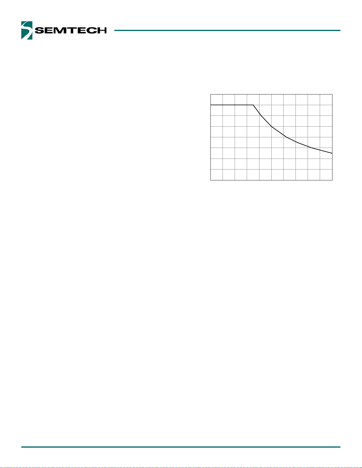
Extending ash mode beyond the 500ms pulse limit could
adversely affect the long term reliability of the SC618.
Flash duration must be derated at higher currents. For
example, 700mA derates to a maximum of 350ms. In
ash mode, I
= 250mV/R
OUT
. Figure 1 shows maximum
ISET
ash mode current for extended duration times.
800
700
600
500
400
300
Flash Current [mA]
200
100
0
0 100 200 300 400 500 600 700 800 900 1000
Flash Duration [ms]
Figure 1 — Maximum Flash Duration
Flash Mode Safety Timer
The SC618 provides a time-out protection function when
in ash mode. The output is disabled if the FLASH pin is
held high for longer than 1 second to protect the LED.
Once this time-out has occurred, the output will stay disabled until the FLASH pin has been pulled low and then
re-enabled.
Spotlight Mode
Spotlight mode is enabled by setting the CTRL pin high
and keeping the FLASH pin low. When in spotlight mode,
the SC618 can maintain a constant current inde nitely to
drive an LED or bank of LEDs. The ISET reference voltage
is set to 100mV so that the output current is maintained
at 200mA when a 0.5 resistor is used. Spotlight current
is always 40% of ash current for any given value of R
In spotlight mode, I
= 100mV/R
OUT
ISET
.
To maximize power efficiency, the SC618 has been
designed to operate in 1x mode when conditions do not
require the charge pump to be active. When rst enabled
the SC618 attempts to regulate the voltage on the ISET
pin in 1x mode. If the voltage on the ISET pin cannot be
maintained and this condition persists for longer than
32ms, then the charge pump will change to 2x mode
operation. In a typical application, the SC618 will operate
in 1x mode until the supply voltage decreases su ciently
ISET
.
9

Applications Information (continued)
SC618
that the voltage on the ISET pin can no longer be maintained. After a 32ms delay (included to prevent false
transitions) the charge pump will convert to 2x mode.
After the charge pump switches from 1x mode to 2x
mode, the device remains in 2x mode until the part is
turned o . If the part is re-enabled in spotlight mode, it
will begin operation in 1x mode and determine the
appropriate mode of operation as previously described.
Protection Circuitry
The SC618 provides several protection features to safeguard the device from catastrophic failures. These features
include:
Input Over-Voltage Protection (IOVP)
•
Output Over-Voltage Protection (OVP)
•
Over-Temperature Protection (OTP)
•
Over-Current Protection (OCP)
•
Short-Circuit Current Protection (SCCP)
•
Input Over-Voltage Protection
IOVP is included to prevent operation at high input voltages that could damage the device. The IOVP circuit
senses the input voltage and determines when the supply
exceeds 6V. Hysteresis is included in this circuit to avoid
chattering between states. When the voltage rises above
this threshold, the device is disabled until the input
voltage drops to a level within the speci ed range.
Output Over-Voltage Protection
Output OVP prevents the SC618 from generating an
output voltage that could damage other devices connected to it such as load LEDs and bypass capacitors.
When the output voltage exceeds 5.5V, the OVP circuit
disables the charge pump until the voltage decreases to
a level within the acceptable range. This circuit allows the
device to drive LEDs with high forward voltages at a
reduced level without exceeding the output voltage
limits speci ed for the device.
Over-Temperature Protection
The OTP circuit prevents the device from overheating and
experiencing a catastrophic failure. When the junction
temperature exceeds 150°C the device is disabled. It
remains disabled until the junction temperature drops
below this threshold. Hysteresis is included to prevent
toggling between modes.
Over-Current Protection
When the SC618 is in 2x mode, the input current will be
approximately double the required output. When the
steady-state load requires the maximum current available in 2x mode, the OCP circuit prevents the device from
overheating from excessive power dissipation. This
feature protects the device when in 1x mode. The current
limit is set lower in the 1x mode due to lower current
requirements.
Short-Circuit Current Protection
SSCP is provided to limit the current that can be sourced
when the output is shorted to ground. When a short
circuit forces V
condition and limits the output current.
to drop below 2V, the SCCP detects the
OUT
Resistor Selection
The ISET resistor selection is critical in generating the
correct current. The value can be chosen to set the spotlight mode current or the ash mode current, and the
two current settings are dependent on the same resistor.
It is recommended that the resistor be selected to match
the desired LED current for ash mode. This allows the
designer to set the SC618’s maximum current and select
the resistor package size necessary for the power dissipation required in ash mode. The typical application
uses a 0.5 resistor to set a ash mode current of 500mA
and spotlight mode current of 200mA. A high precision
resistor should be used to ensure the speci ed accuracy
for LED current.
To avoid malfunction of the charge pump, it is recommended that the resistance seen at the ISET pin remain
constant while the device is active (flash or spotlight
mode). Changing the resistance value or the load current
while the device is active could cause instability.
Capacitor Selection
The SC618 is designed to use low-ESR ceramic capacitors
for the input and output bypass capacitors as well as the
charge pump bucket capacitors. Ideal performance is
achieved when C1 is exactly equal to C2. It is recommended that X5R or X7R ceramic capacitors be used for
best performance.
10

Applications Information (continued)
SC618
PCB Layout Considerations
The following layout is suggested for a two-layer design.
The capacitors C1 and C2 are the bucket capacitors and
each conducts the full load current of up to 500mA pulsed
for one half clock cycle. C3 is the output decoupling
capacitor placed near the VOUT pin. C4 is the input
decoupling capacitor placed near the VIN pin. Multiple
vias should be used whenever it is necessary to change
layers on nets connecting to pins VIN, VOUT, GND, C1-,
C1+, C2- and C2+.
The load current return path is from the ISET sense point
through the resistor and back to the ground pins.
Resistance in this path adds to the total resistance and
has the e ect of reducing the LED current by about 4%
per 10mV of DC drop across the return copper trace in
ash mode. For this reason, it is crucial to have a low resistance return path. Place and ground the resistor as close
as possible to the ground pin of the SC618. The trace from
the ISET pin has virtually no current. The ISET trace should
make contact at the pad of the power sense resistor to
minimize the effect of voltage drop between the LED
cathode and the resistor.
while in ash or spotlight mode. It is critical to maintain
adequate ground plane around the device to maximize
heat transfer and avoid over-temperature shutdown.
Resistor R1 is routed with a very low resistance connection between R1 and GND pin 3. The sense trace between
Pin 6 and R1 is routed around the ground vias, allowing
the shortest ground return path possible. The sense trace
is connected to R1 at the positive terminal pad for the
most accurate output possible. The bottom copper layer
is mostly a ground plane with no obstructions between
the ground vias. The smaller rectangle to the left connects the input power to VIN pin 1 and input capacitor
C4. The two traces at the lower left are for logic inputs
FLASH and CTRL. The trace to the right is the ISET pin
sense trace. The sense trace is routed out of the path of
the returning ground current.
Thermal Resistance Considerations
The SC618 package is thermally e cient when the circuit
board layout connects the thermal pad through multiple
vias to the ground plane. The thermal resistance is rated
at 49°C/W, and this rating is dependent on the connection between the thermal pad and the ground plane. The
layout should keep the junction temperature below the
OTP limit while operating the SC618 within the speci ed
electrical conditions for I
allow the junction temperature to reach the OTP limit
OUT
and V
. A poor layout may
ISET
11

Outline Drawing — MLPD-UT-10
SC618
PIN 1
INDICATOR
(LASER MARK)
aaa
LxN
A
C
1
E
A1
C
2
A2
B
DIM
MIN
.018
A
.000
A1
A2
b
E
A
SEATING
PLANE
C
D
.007
C
.074 .079 .083 1.87 2.02
D
.042
E
.114
e
L
N
aaa
bbb
DIMENSIONS
INCHES
MAXNOM
-
.024
-
(.006)
.002 0.00
.009
.011
.048
.052
.118
.122
10
.003
.004 0.10
MILLIMETERS
MIN MAX
0.45
0.18
1.06
2.90 3.00 3.10
0.30.012 .020.016 0.40 0.50
NOM
-
-
(0.1524)
0.23
1.21
0.50 BSC.020 BSC
10
0.08
0.60
0.05
0.30
2.12
1.31
N
e
NOTES:
1.
CONTROLLING DIMENSIONS ARE IN MILLIMETERS (ANGLES IN DEGREES).
2.
COPLANARITY APPLIES TO THE EXPOSED PAD AS WELL AS TERMINALS.
bxN
bbb C A B
12

Land Pattern — MLPD-UT-10
SC618
K
(C)
H
X
P
NOTES:
1.
THIS LAND PATTERN IS FOR REFERENCE PURPOSES ONLY.
CONSULT YOUR MANUFACTURING GROUP TO ENSURE YOUR
COMPANY'S MANUFACTURING GUIDELINES ARE MET.
THERMAL VIAS IN THE LAND PATTERN OF THE EXPOSED PAD
2.
SHALL BE CONNECTED TO A SYSTEM GROUND PLANE.
FAILURE TO DO SO MAY COMPROMISE THE THERMAL AND/OR
FUNCTIONAL PERFORMANCE OF THE DEVICE.
G
Z
Y
DIMENSIONS
DIM MILLIMETERS
C
G
H
K
P
X
Y
Z
INCHES
(.112)
.075 1.90
.055
.087
.020
.012
.037
.150
(2.85)
1.40
2.20
0.50
0.30
0.95
3.80
Contact Information
Semtech Corporation
Power Management Products Division
200 Flynn Road, Camarillo, CA 93012
Phone: (805) 498-2111 Fax: (805) 498-3804
www.semtech.com
13
 Loading...