

United States Patents: 6,504,422, 6,794,926
www.semtech.com
1
POWER MANAGEMENT
SC606
Low Noise Smart LED
Driver with Serial Interface
Description
August 31, 2006
Applications
Features
The SC606 is a very high efficiency charge pump white/color LED
driver from the mAhXLife
TM
family of products. It is optimized for
Li-Ion battery applications. The LED current is regulated to a value
configured by the user through an I2C compatible serial interface.
LED outputs are current-matched for consistent LED brightness.
Up to 6 LEDs are controlled in three zones for brightness control in
multiple displays. The 6 LED outputs are divided into 3 pairs of
LEDs. Each pair has current that is programmable independent of
the other pairs. Any combination of LEDs may be turned on using
the serial interface. The SC606 also has a float detect feature
that disables any current driver during normal operation when an
open-load condition is detected.
Patented low noise switching circuitry and constant output current
allow the use of extremely small input and output capacitors.
Very High Efficiency Over 90% of Battery Life
Current Regulation for 6 LEDs
Current Matching Tolerance of +/- 3.5% from LED to LED
Current Accuracy to +/- 6.5% of Specified Value
Current Range per LED [0.5mA - 32mA]
High Available Total LED Current = 6
I
LED
= 120mA
I2C Bus Limited Compatibility SC606
Low Shutdown Current: 0.1μA Typical
Soft-Start /In-rush Current Limiting
Short Circuit /Thermal Protection
MLP-16 [4x4] Package
1.33MHz and 250kHz Programmable Fixed Frequency
Separate Brightness Zones for Multiple Displays
Three Charge Pump Modes of Operation: 1x, 1.5x and 2x
Open LED Output Protection
Cellular Phones
LED Backlighting
PDA Power Supplies
Portable Devices
Electronic Books
Wireless Web Appliances
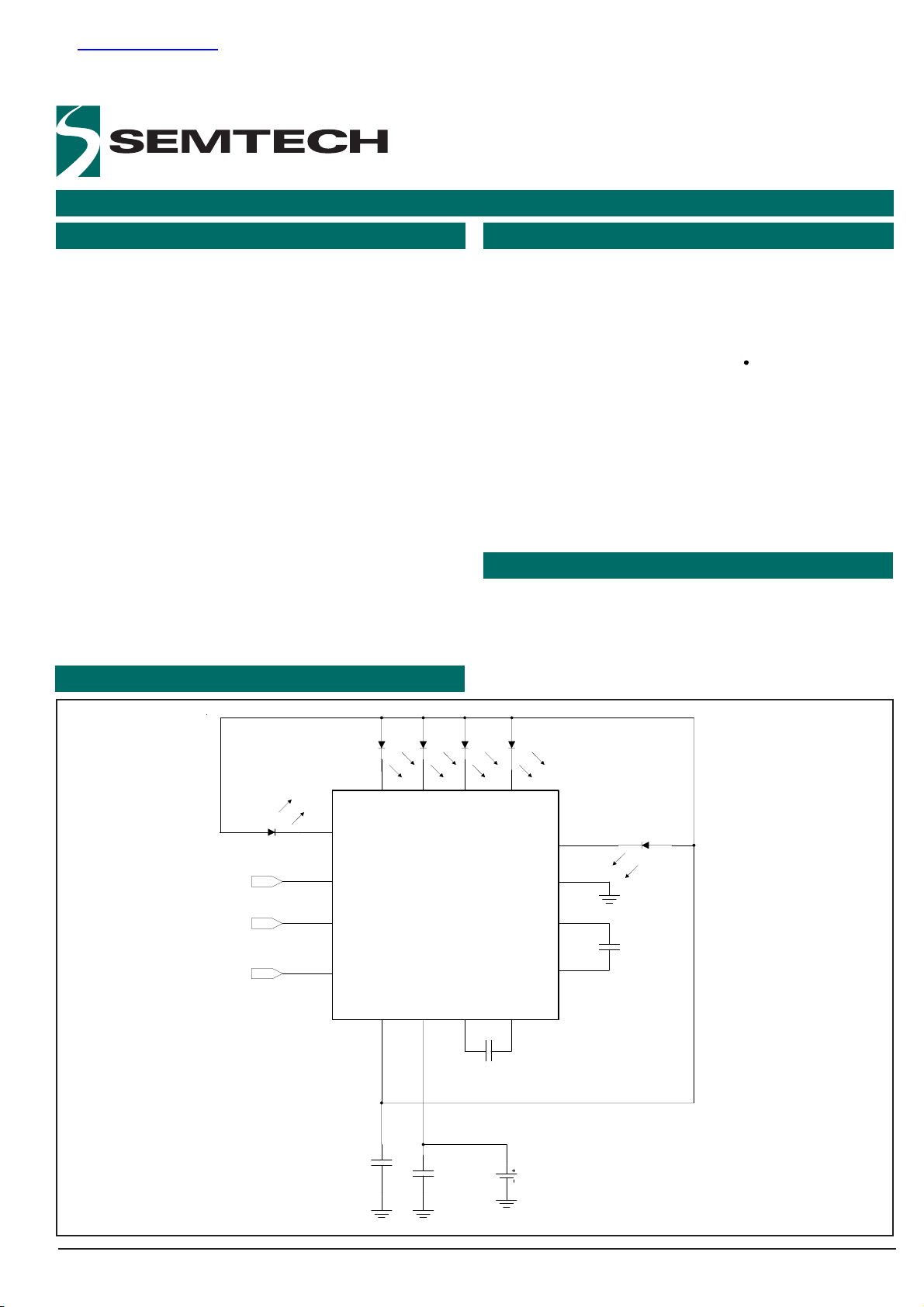
Typical Application Circuit
C3
1µF
C4
1µF
VBAT
1
2
3
4
5
6
7
8
9
10
SCL
SDA
EN
C2
1µF
VOUT
VIN
C1-
C1 +
C2-
C2+
GND
ILEDC2
ILEDA1
SDA
SCL
EN
ILEDA2
ILEDB2
ILEDC1
ILEDB1
D1
SC606
11
12
13
14
15
16
C1
1µF
D6
D5D4D3D2
Patent Pending
查询SC606供应商

2© 2005 Semtech Corp. www.semtech.com
POWER MANAGEMENT
SC606
Absolute Maximum Ratings
Electrical Characteristics
Unless specified: TA = -40°C to 85°C, VIN= 2.85V to 5.5V, C1 = C2 = C3 = C4 = 1.0μF (ESR = 0.03Ω), Typical values @ TA =25°C, LED VF = 3.4V
This device is ESD sensitive. Use of standard ESD handling precautions is required.
retemaraPlobmySnoitidnoCniMpyTxaMstinU
tnerruCtnecseiuQI
Q
I,edomx1
TUO
V,Am0=
NI
V2.4=00510002Aµ
I,edomx2dnaedomx5.1
TUO
Am0=34Am
V,0=elbanE
NI
V2.4=1.07 Aµ
ycaruccAtnerruCDEL
I
RRE-DEL
Am5.0 ≤ I
nDEL
≤ Am0.4
)2()1(
V2.3 ≤ VNI≤ V2.4
062-001±062Aµ
Am5.4 ≤ I
nDEL
≤ Am51
V2.3 ≤ V
NI
≤ V2.4
5.6-2±5.6%
Am5.51 ≤ I
nDEL
≤ Am23
)3(
V2.3 ≤ VNI≤ V2.4
9-3±9
%
gnihctaMtnerruC
I
DEL-ot-DEL
Am5.0 ≤ I
nDEL
≤ Am0.4
)2(
V2.3 ≤ VNI≤ V2.4
041-05±041Aµ
Am5.4 ≤ I
nDEL
≤ Am51
V2.3 ≤ V
NI
≤ V2.4
3-1±3%
Am5.51 ≤ I
nDEL
≤ Am23
)3(
V2.3 ≤ VNI≤ V2.4
57.3-5.1±57.3%
gnillafedomx5.1otedomx1V
X1SNART
I
TUO
I,Am06=
nDEL
Am01=
)1(
85.3V
gnillafedomx2otedomx5.1
egatlovnoitisnart
V
X5.1SNART
I
TUO
I,Am06=
nDEL
Am01=
)1(
89.2V
retemaraPlobmySmumixaMstinU
egatloVylppuSV
NI
0.6+ot3.0-V
egatloVtuptuOV
TUO
0.6+ot3.0-V
noitaruDtiucriCtrohSTUOVCSetinifednI
tneibmAotnoitcnuJ,ecnatsiseRlamrehT
)1(
θ
AJ
04W/C°
esaCotnoitcnuJ,ecnatsiseRlamrehT
θ
CJ
4.2W/C°
tneibmAgnitarepOT
A
58+ot04-C°
egnaRerutarepmeTnoitcnuJT
CJ
051+ot04-C°
egnaRerutarepmeTegarotST
GTS
051+ot56-C°
TRTLMIA606CSerutarepmeTwolfeRRIT
DAEL
062C°
Exceeding the specifications below may results in permanent damage to the device or device malfunction.
Operation outside of the parameters specified in the Electrical Characteristics section is not required.
1) Calculated from package in still air, mounted to 3” x 4.5”, 4 layer FR4 PCB with thermal vias under the exposed pad per JESD51 standards.

3© 2005 Semtech Corp. www.semtech.com
POWER MANAGEMENT
SC606
Electrical Characteristics (Cont.)
retemaraP
lobmySnoitidnoCniMpyTxaMstinU
ycneuqerFrotallicsOf
CSO
=retsigeRsutatS#FFO/NO
XXXXX1X
)4(
31.133.135.1zHM
ycneuqerFrotallicsOf
CSO
=retsigeRsutatS#FFO/NO
XXXXX0X
)4(
5.2120525.782zHk
timiLtnerruCtupnI
)2(
I
TIMIL
V2.3 ≤ VNI≤ V2.4
VmorfdeilppatiucrictrohS
TUO
DNGot
022058Am
dlohserhThgiHtupnIV
HI
dlohserhtcigolhgihtupnI6.1V
dlohserhTwoLtupnIV
LI
dlohserhtcigolwoltupnI4.0V
tnerruChgiHtupnII
HI
VHIV=
NI
01Aµ
tnerruCwoLtupnII
LI
VLI=DNG01Aµ
I
2
ecafretnIC
Iedomevalshtiwecnailpmocdetimil
2
IspilihPtamroFdenibmoCC
2
0002,yraunaJdetad1.2noisrevnoitacificepsC
egatloVtupnIlatigiD
V
LI
4.0V
V
HI
6.1
leveLwoLtuptuOADSV
LO
I
NID
Am3=)ADS(
4.0
V
I
NID
Am6=)ADS(
6.0
V
tnerruCtupnIlatigiDI
GD
2.0-2.0Aµ
ecnaticapaCniPO/IC
NI
01Fp
I
2
gnimiTC
ycneuqerFkcolCf
LCS
004044zHk
doirePwoLLCS
t
woL
3.1sµ
doirePhgiHLCS
t
hgiH
6.0
sµ
emiTdloHataDt
TAD_DH
0sµ
emiTputeSataDt
TAD_US
001sn
detaepeR-emiTputeS
noitidnoCtratS
t
ATS_US
6.0sµ
detaepeR-emiTdloH
noitidnoCtratS
t
ATS_DH
6.0sµ
rofemiTputeS
noitidnoCpotS
t
ATS_US
6.0sµ

4© 2005 Semtech Corp. www.semtech.com
POWER MANAGEMENT
SC606
retemaraP
lobmySnoitidnoCniMpyTxaMstinU
neewteBemiTeerF-suB
TRATSdnaPOTS
t
FUB
3.1sµ
emiTpu-tratSecafretnI
t
NE
(emiTpu-tratSsuB
dellupsiNEretfa)hgih
053sµ
Electrical Characteristics (Cont.)
Notes:
1) I
LEDn
= any LED’s current from D1, D2, D3, D4, D5 and D6.
2) Guaranteed by design.
3) Maximum total of LED currents not to exceed 120mA.
4) X = Don’t care.

5© 2005 Semtech Corp. www.semtech.com
POWER MANAGEMENT
SC606
Pin Configuration Ordering Information
Pin Descriptions
niPemaNniPnoitcnuFniP
11ADELI .)dednuorgronepotfelebyamnip,esunitonfl(1ADELrofknistnerruC
2ADS.enilatadlaires
lanoitcerid-iB
3LCS.tupnikcolcsublaireS
4NE .wolsiNEnehwFμ1.0yllacipytsitnerrucsaiB.elbanehgihevitcA
5TUOV .dn
uorgotTUOVmorfroticapacFμ1atcennoC.pmupegrahcehtfotuptuO
6NIV
ecnamrofrepdevorpmiroF.dnuorgotNIVmorfroti
capacFμ1atcennoC.egatlovtupnI
.Fμ01~Fμ7.4otroticapacehtesaercni,edomx5.1dnazHk052gnisunehw
7-1C.1roticapa
ctekcubfolanimretevitageN
8+1C.1roticapactekcubfolanimretevitisoP
9-2C.2roticapactekcubfolanimretevitageN
01+
2C.2roticapactekcubfolanimretevitisoP
11DNG.dnuorG
212CDELI .)dednuorgronepotfelebyamnip,esunitonfl(2CDELrof
knistnerruC
311CDELI .)dednuorgronepotfelebyamnip,esunitonfl(1CDELrofknistnerruC
412BDELI .)dednuorgronepot
felebyamnip,esunitonfl(2BDELrofknistnerruC
511BDELI .)dednuorgronepotfelebyamnip,esunitonfl(1BDELrofknis
tnerruC
612ADELI .)dednuorgronepotfelebyamnip,esunitonfl(2ADELrofknistnerruC
TdaPlamrehT
.saivelpitlumgnisu
enalpdnuorgottcennoC.sesoprupgniknistaehrofdaP
.yllanretnidetcennoctoN
ECIVEDEGAKCAP
)1(
TRTLMIA606CS
)2(
61-4x4PLM
BVEA606CSdraoBnoitaulavE
Notes:
1) Available in tape and reel only. A reel contains 3000 devices.
2) Available in lead-free package only. This product is fully WEEE
and RoHS compliant.
TOP VIEW
1
2
3
4
12
11
10
9
16 15 14
13
5678
MLP16: 4X4 16 LEAD
T
ILEDA1
SDA
SCL
EN
ILEDA2
ILEDB1
ILEDB2
ILEDC1
ILEDC2
GND
C2+
C2-
VOUT
VIN
C1-
C1+

6© 2005 Semtech Corp. www.semtech.com
POWER MANAGEMENT
SC606
VIN
ILEDA2
EN
6
12
13
5
C1+ C2-
C1-
mAhXLife Fract ional Charge Pump
[1x, 1.5x, 2x]
Schmitt Buffer
1.33MHz /250kHz
Oscil lator
Mode Sel ect
[1x, 1.5x, 2x
Star tup, Shutdo wn]
Current Brightness Control
Current Sense FETs
and Amplifier(s)
ILEDA1
ILEDC1
ILEDB2
ILEDB1
ILEDC2
7
9
10 16
11
1
15
14
VOUT
C2+
4
2
3
Schmitt Buffer
Schmitt Buffer
Serial I/O Logi c
Current Set / DAC
Regist ers
TM
GND
SCL
8
SDA
Block Diagram

7© 2005 Semtech Corp. www.semtech.com
POWER MANAGEMENT
SC606
Detailed Description
The SC606 contains a fractional charge pump, mode selection
circuit, serial I/O logic, serial data registers and current regulation
circuitry for 6 LED outputs. All are depicted in the Block Diagram
on page 6.
The fractional charge pump multiplies the input voltage by 1, 1.5
or 2 times the input voltage. The charge pump switches at a fixed
frequency that is bit selectable to 1.33MHz or 250kHz. The default
frequency is 1.33MHz. 250kHz may require additional input
capacitance of up to 10μF. The charge pump does not switch
during 1x mode, saving power and improving efficiency.
The mode selection circuit automatically selects the mode as 1x,
1.5x or 2x based on circuit conditions such as LED voltage, input
voltage and load current. 1x is the most efficient mode, followed
by 1.5x and 2x modes. At lower voltages a stronger mode may be
needed to maintain regulation. If so , the mode will change first to
1.5x and then later to 2x. 2x mode usually operates for a much
shorter run time compared to 1x mode, and 2x mode maintains
the output until the battery is discharged to 2.85V or less. The LED
requiring the highest voltage drop will determine the output voltage
needed to drive all outputs with sufficient anode voltage.
Comparing all cathodes and regulating VOUT for the LED with the
lowest cathode voltage ensures sufficient bias for all LEDs.
The LED outputs are controlled through the serial data registers,
found on page 10 in Table 1. LED on/off functions are
independently controlled, so that any combination of LEDs may be
switched on. LED current is set per LED pair. For example, when
ILEDA1 and ILEDA2 are both on, ILEDA1 = ILEDA2. But ILEDA1 and
ILEDA2 do not have to be on at the same time.
Six (6) current regulating circuits sink matched currents from the
LEDs on a per pair basis. LEDs with matched forward voltage will
produce the best possible matched currents. For best matching
performance it is recommended that the LED to LED difference,
ΔV
F
, be under 250mV.
Designing for Lowest Possible Battery Current
The battery current and efficiency of the SC606 are mostly
dependent on the charge pump mode of operation. To get the
best performance from the SC606 it is better to use LEDs with
consistantly lower VF voltage. Lower VF will keep the charge pump
in 1x mode longer and will use less battery current, extending the
run time of the battery.
Mode transition voltages V
TRANS1X
and V
TRANS1.5X
can be estimated
by the following equations:
Applications Information
V
TRANS1X
= VF + V
ILEDn
+(# of LEDs used) I
LED
0.83
V
TRANS1.5X
= [VF + V
ILEDn
+(# of LEDs used) I
LED
10.1]/1.5
where, VF is the anode to cathode voltage and V
ILEDn
is the voltage
at the ILED pin. Typically V
ILED
=120mV and I
LED
is the LED current.
Power efficiency can be estimated for the intended battery voltage
range.
η = [V
OUTIOUT
/ VIN(I
OUT
Mode+IQ)] 100 %
where, VOUT = VF+ V
ILEDn
and IQ = 1.5mA, in 1x mode
IQ = 3mA, in 1.5x or 2x mode
Quiescent Current
IQ at no load will vary with the device state. A sequence of steps is
now described which will demonstrate the effect that the device
state has on IQ when VIN = 3.8V.
(1) After power up (Enable High) and before any serial
communication, the IQ is approximately 2.2mA. This is because
the output defaults to 5V and the charge pump is active to support
the 5V. The charge pump also defaults to 1.33MHz.
(2) After power up if the clock is changed to 250kHz, the IQ will
decrease to 1mA.
(3) If one LED is set on at 0.5mA, the input current will be 1.5mA.
For a typical white LED, the 5V output is much higher than
necessary, so the charge pump will switch off and the output will
adjust to a normal value for the LED, typically around 3.5V.
(4) Turn off the LED and IQ = IIN = 80μA with Enable = High. This is
the lowest power state while Enable = High.
I
LED
Accuracy
I
LED
is determined by the status of registers at 00h, 01h and 02h.
The tolerance of the I
LED
current is +/-6.5% at the 10mA setting.
For example, if the data registers are configured so that each LED
current should be 10mA, the actual LED currents would be between
9.35mA and 10.65mA (+/-6.5%). All 6 outputs meet this
requirement over the industrial temperature range. To calculate
the error I
LED-ERR
[%], use the formula,
I
LED-ERR
[%] = ±
I
LED(measured) -ILED
I
LED
100%

8© 2005 Semtech Corp. www.semtech.com
POWER MANAGEMENT
SC606
Applications Information (Cont.)
Current Matching
Current Matching refers to the ΔI from an LED compared to the
average of the minimum and maximum value of all LEDs that are
programmed for the same current.
I
LED-LED-ERR
[%]
= =
= =
=
I
MAX
I
MAX
+ I
MIN
-1
100%
2
or
I
MIN
I
MAX
+ I
MIN
-1
100%
2
which reduces to
± ±
± ±
±
I
MAX -IMIN
I
MAX
+ I
MIN
100%
1x Mode, 1.5x Mode and 2x Mode
1x Mode, 1.5x Mode and 2x Mode all refer to the charge pump
configuration. These modes multiply the input voltage and ensure
that V
OUT
is high enough for current to be regulated in the LEDs.
Mode Transition Voltage
Mode transition voltage refers to the input voltage at the point
when the charge pump changes from a weaker mode (lower
numerically) to a stronger mode (higher numerically). V
TRANS1X
is
the transition from 1x to 1.5x mode, and V
TRANS1.5X
is the
transition from 1.5x to 2x mode.
9© 2005 Semtech Corp. www.semtech.com
POWER MANAGEMENT
SC606
I2C Communication
The SC606 interface uses a limited version of the combined
format protocol as described in the Phillips I2C Bus Specification
version 2.1. With this format, the Start condition and the Slave
Address are both repeated. Data formatting must be a single byte
only. Note that the SC606 can only operate on an I2C bus using
the limited combined format protocol. If any other I2C data
formatting is used on the bus the SC606 may exhibit false
acknowleges to the commands. The I2C Slave Address is
1100110. I2C Fast Mode is supported at 400kbit/s. For more
information about the I2C combined protocol refer to the I2C Bus
Specification from Philips Semiconductors.
Slave Address
Following a start condition, the bus master outputs the address
of a slave device. The 7 bit slave address for the SC606 is
1100110. The address is followed by a least significant bit (LSB).
The LSB determines the data direction.
Data Formatting
Write FormatWrite Format
Write FormatWrite Format
Write Format
Read FormatRead Format
Read FormatRead Format
Read Format
S : Start Condition
W : ‘0’ = Write
R : ‘1’ = Read
A : Acknowledge, sent by slave
B : Acknowledge, sent by master
Sr : Repeated Start Condition
P : Stop Condition
Slave Address: 7 bit
Register Address: 8 bit
Data: 8 bit
Applications Information (Cont.)
SsserddAevalSWA etyB1
sserddAretsigeR
ArSsserddAevalSWAylnOetyB1
ataDn
AP
SsserddAevalSWAetyB1
sserddAretsigeR
ArSsserddAevalSRAylnOetyB1
ataDn
BP
BSM BSL
1 100110 W/R

10© 2005 Semtech Corp. www.semtech.com
POWER MANAGEMENT
SC606
emaNretsigeR
retsigeR
tib-8[sserddA
]lamicedaxeH
elbaTnoitcnuFtiB'sretsigeR
7B6B5B4B3B2B1B0B
geR21A_DELh00
XX 11egaPno
2elbaTotrefeRgeR21B_DELh10
geR21C_DELh20
geR#FFO/NOh300
ycneuqerF
zHk052=1
zHM33.1=0
2CDEL
nO=1
ffO=0
1CDEL
nO=1
ffO
=0
2BDEL
nO=1
ffO=0
1BDEL
nO=1
ffO=0
2ADEL
nO=1
ffO=0
1ADEL
nO=1
ffO=0
Table 1 - SERIAL DATA REGISTERS
Note: X = Don’t care
1 = Logic High
0 = Logic Low
Applications Information (Cont.)

11© 2005 Semtech Corp. www.semtech.com
POWER MANAGEMENT
SC606
tnerruCDEL
]Am[
7B6B5B4B3B2B1B0BlamiceD
5.61 XX 100000 23
0.71 XX 100001 33
5.71 XX100010 43
0.81 XX100011 53
5.81 XX100100 63
0.91 XX100101 73
5.91 XX100110 83
0.02 XX100111 93
5.02 XX101000 04
0.12 XX101001 14
5.12 XX101010 24
0.22 XX101011 34
5.22 XX101100 44
0.32 XX101101 54
5.
32 XX101110 64
0.42 XX 101111 74
5.42 XX110000 84
0.52 XX110001 94
5.52 XX110010 05
0.62 XX110011 15
5.62 XX 110100 25
0.72 X X 110101 35
5.72 XX110110 45
0.82 XX110111 55
5.82 XX111000 65
0.92 XX111001 75
5.92 XX111010 85
0.03 XX 111011 95
5.03 XX 111100 06
0.13 XX 111101 16
5.13 XX 111110 26
0.23 XX 111111 36
tnerruCDEL
]Am[
7B6B5B4B3B2B1B0BlamiceD
5.0 XX000000 0
0.1 XX000001 1
5.1 XX000010 2
0.2 XX000011 3
5.2 XX000100 4
0.3 XX000101 5
5.3 XX000110 6
0.4 XX000111 7
5.4 XX001000 8
0.5XX0010019
5.5 XX001010 01
0.6 XX001011 11
5.6XX00110021
0.7XX00110131
5.7 XX001110 41
0.8 XX001111 51
5.8 XX010000 61
0.9 XX010001 71
5.9XX01001081
0.01XX01001191
5
.01 XX0 1010 0 02
0.11 XX 01010 1 12
5.11XX01011022
0.21 XX010111 32
5.21 XX011000 42
0.31 XX011001 52
5.31XX01101062
0.41XX01101172
5.41 XX0 11100 82
0.51 XX011101 92
5.51 XX011110 03
0.61 XX0 11111 13
Note: X = Don’t care
Table 2 - DAC Codes For LED Output Current
Applications Information (Cont.)

12© 2005 Semtech Corp. www.semtech.com
POWER MANAGEMENT
SC606
Typical Characteristics
Ripple in 1x Mode for 6 LEDs at 20mA Startup
1.33MHz Ripple in 1.5x Mode for 6 LEDs at 20mA
250kHz Ripple in 1.5x Mode for 6 LEDs at 20mA
Ch1 50mV/DIV
Ch2 50mV/DIV
Ch3 2V/DIV
Ch4 100mA/DIV
400 ns/DIV
Ch1 50mV/DIV
Ch2 50mV/DIV
Ch3 2V/DIV
Ch4 100mA/DIV
400 ns/DIV
Ch1 50mV/DIV
Ch2 50mV/DIV
Ch3 2V/DIV
Ch4 100mA/DIV
2 us/DIV
Ch1 1V/DIV
Ch2 1V/DIV
Ch3 5V/DIV
Ch4 500mA/DIV
100 us/DIV
Efficiency for 6 LEDs at 20mA and 3.31V Efficiency for 6 LEDs at 10mA and 3.31V
50
60
70
80
90
100
3.23.43.63.844.2
Input Voltage [V]
Efficiency [%]
TA = 25°C
50
60
70
80
90
100
3.23.43.63.844.2
Input Voltage [V]
Efficiency [%]
TA = 25°C

13© 2005 Semtech Corp. www.semtech.com
POWER MANAGEMENT
SC606
1.33MHz Ripple in 2x Mode for 6 LEDs at 20mA
250kHz Ripple in 2x Mode for 6 LEDs at 20mA
Ch1 50mV/DIV
Ch2 50mV/DIV
Ch3 2V/DIV
Ch4 100mA/DIV
400 ns/DIV
Ch1 50mV/DIV
Ch2 50V/DIV
Ch3 2V/DIV
Ch4 100mA/DIV
2 us/DIV
Typical Characteristics (Cont.)
IQ, LEDs Turned Off
83
86
89
92
95
2.85 3.38 3.91 4.44 4.97 5.5
Battery Voltage [V]
Quiescent Current [uA]

14© 2005 Semtech Corp. www.semtech.com
POWER MANAGEMENT
SC606
Evaluation Board Schematic
1
2
C11
10uF
A2
C1 C2
VOUT
VOUT
VIN
1
TP5
GND
1
TP6
GND
1
TP7
GND
VIN
1
TP8
GND
POS
1
NEG
2
J1
1 2
C1
1uF
1
2
C2 1uF
ILEDA1
1
SDA
2
SCL
3
EN
4
VOUT5VIN
6
GND
11
ILEDC2
12
ILEDC1
13
ILEDB2
14
ILEDB1
15
ILEDA2
16
C2+
10
C1-
7
C2-
9
C1+
8
SC606A
B1
B2
P0.0
1
P0.1
2
P0.2
3
P0.3
4
P1.0
5
P1.2
6
VSS
7
VPP
8
CEXT
9
XI N10XOU T
11
VCC
12
D-
13
D+
14
P1.3
15
P1.1
16
P.7
17
P.6
18
P.5
19
P.4
20
U4
Delc om 8022 00
Y1
Ceramic Res. 6MHz
1
1
2
2
3
3
4
4
U5
USB_Ty pe-B
F11A
SDA
1 2
R7
7.5k
1
2
C5
4.7uF
1
2
C7
.1uF
SCL
EN
12
R8
150
12
D7
USB Power
C1-
1
2
C3
1uF
C1+
1
TP1 1
A2
1
TP12
A1
C2-
1
TP13
SDA
1
TP1 4
SCL
1
TP15
EN
C2+
1
TP16
VOUT
1
TP17
VIN
1
TP1 8
C1-
1
TP1 9
C1+
1
TP20
C2-
1
TP21
C2+
1
TP22
GND
1
TP23
C2
1 2
JP9
1 2
JP10
1
TP2 4
C1
1
TP25
B2
1 2
JP11
1
TP26
B1
1 2
JP12
1 2
JP13
1 2
JP14
A1
SDA
SCL
EN
12
R5
1ohm
12
R4
1ohm
12
R3
1ohm
12
R2
1ohm
12
R1
1ohm
12
R6
1ohm
1
2
C4 1uF
1
2
3
JP8
BERG_3PI N
Enable
12
JP6
VOUT
12
JP5
12
JP4
12
JP3
12
JP2
12
JP1
12
D1
LED_1206
12
D2
LED_1206
12
D3
LED_1206
12
D4
LED_12 06
12
D5
LED_1206
12
D6
LED_1206

15© 2005 Semtech Corp. www.semtech.com
POWER MANAGEMENT
SC606
ITEM QUANTITY REFERENCE PART
________________________________________________________________________
1 4 C1,C2,C3,C4 1UF X5R
2 1 C5 4.7UF
3 1 C7 .1UF
4 1 C11 10UF
5 6 D1,D2,D3,D4,D5,D6 LED_1206 NICHIA NSCW100
6 1 D7 USB POWER
7 1 F1 1A
8 12 JP1,JP2,JP3,JP4,JP5,JP6, 2PIN JUMPER
JP9,JP10,JP11,JP12,JP13,
JP14
9 1 JP8 3PIN JUMPER
10 1 J1 BATTERY INPUT
11 6 R1,R2,R3,R4,R5,R6 1OHM
12 1 R7 7.5K
13 1 R8 150
14 5 TP5,TP6,TP7,TP8,TP22 GND
15 1 TP11 A2
16 1 TP12 A1
17 1 TP13 SDA
18 1 TP14 SCL
19 1 TP15 EN
20 1 TP16 VOUT
21 1 TP17 VIN
22 1 TP18 C1-
23 1 TP19 C1+
24 1 TP20 C2-
25 1 TP21 C2+
26 1 TP23 C2
27 1 TP24 C1
28 1 TP25 B2
29 1 TP26 B1
30 1 U1 SC606
31 1 U4 DELCOM 802200
32 1 U5 USB_TYPE-B
33 1 Y1 CERAMIC RES. 6MHZ
Evaluation Board Bill of Material

16© 2005 Semtech Corp. www.semtech.com
POWER MANAGEMENT
SC606
Evaluation Board Gerber Plots

17© 2005 Semtech Corp. www.semtech.com
POWER MANAGEMENT
SC606
Outline Drawing - MLP-16 [4x4]
Marking Information
yyww = Datecode (Example: 0422)
Marking for SC606AIML
606A
yyww
INDICATOR
(LASER MARK)
PIN 1
DIMENSIONS
NOM
INCHES
N
bbb
aaa
A2
A1
E1
D1
DIM
L
e
E
D
A
b
MIN MAX
MILLIMETERS
MINMAX NOM
.153 .157 .161 3.90 4.00 4.10
.153 .157 .161 3.90 4.00 4.10
E1
.003
.010
.079
16
.012
.085
-
.000
.031
(.008)
0.08
0.30
16
.014
.089
0.25
2.00
.040
-
.002-0.00
0.80
2.25
0.35
2.15
-
0.05
1.00
(0.20)
.004 0.10
2.00 2.15 2.25
0.65 BSC.026 BSC
0.30.012 .020.016 0.40 0.50
.089.085.079
D/2
2
A
A1
1
LxN
bbb C A B
A2
bxN
e
SEATING
PLANE
C
E/2
D1
N
e/2
aaa
C
CONTROLLING DIME NSIONS ARE IN MILLIMETERS (ANGLES IN DEGREES).
COPLANARITY APPLIES TO THE EXPO SED PAD AS WELL AS THE TERMINALS.
1.
2.
NOTES:
A D
E
B
-
--
-

18© 2005 Semtech Corp. www.semtech.com
POWER MANAGEMENT
SC606
Land Pattern - MLP-16 [4x4]
Semtech Corporation
Power Management Products Division
200 Flynn Road, Camarillo, CA 93012
Phone: (805) 498-2111 FAX (805)498-3804
Contact Information
Visit us at: www.semtech.com
P
Y
K
C
Z
P
Y
X
G
K
H
.189
.026
.016
.033
.122
.091
.091
4.80
0.40
0.85
0.65
2.30
2.30
3.10
DIM
(3.95)
MILLIMETERS
DIMENSIONS
(.156)
INCHES
THIS LAND PATTERN IS FO R REFERENCE PURPOSES ONLY.
CONSULT YOUR MANUFACTURIN G GROUP TO ENSURE YOUR
COMPANY'S MANUFACTURING GUIDELINES ARE MET.
NOTES:
1.
2x G
H
2x (C)
2x Z
X
 Loading...