


www.semtech.com1
POWER MANAGEMENT
SC600
mAhXLifeTM LED Driver with
5.0V, 4.5V, or 4.0V Output
50
60
70
80
90
100
3.03.23.43.63.84.04.2
Inpu t Vo l t age [V]
Efficiency [%]
90% of Li-Ion
Battery Life
SC600A
5.0V@60mA
Device w ith Only 2x Mo de
5.0V@60mA
January 9, 2006
Description
Features
Typical Application Circuit
Applications
Features
The SC600 is a versatile charge pump designed for use
in battery operated power supply applications. The wide
input range is matched for Li-Ion battery applications.
mAhxLife
TM
LED Drivers feature a fractional charge pump
implementation with effi ciency comparable to a switching
regulator without costly inductors. Only two tiny ceramic
capacitors are required, and the inductorless implementation provides a reduced-EMI solution. Patented low
noise mode switching circuitry and constant output current allow the use of extremely small input and output
capacitors.
The SC600 charge pump can be used for applications
that require up to 120mA of output current with a 4.0V
or 4.5V output. The 5.0V output version provides up to
60mA of output current.
mAhXLifeTM LED drivers replace switched mode power
supplies and provide comparable effi ciency with less cost,
area, noise, and complexity.
Typical Effi ciency
Small size - MLPD 10 lead 3x3mm or MSOP-10
package allows for a complete solution in .05 sq. in.
Peak effi ciency over 90% (extends battery life)
Four component versions available
60mA versions available in 5.0V and 4.5V output
120mA versions available in 4.5V and 4.0V output
Short-circuit and over-temperature protection
Soft-start function
Shutdown current <1μA
Selectable fi xed frequencies of 8kHz, 32kHz,
262kHz and 650kHz
Low input and output ripple
Regulated to ± 5%
Ease of use
Cellular phones
LED backlighting
PDA power supplies
Portable electronics
Electronic books
Handheld computers
Wireless web appliances
Cin
1.0 uF
2.7 V t o 6. 5V
Cbucket1
1.0 uF
Cbucket 2
1.0 uF
VIN
EN
CD4
CX8
GND
CF2-
CF2+
CF1-
CF1+
VOUT
3
6
4
5
8
7
10
9
2
1
U1
SC600
Cout
0.3 3uF
UP TO 6 LEDS
4.0 V, 4. 5V o r 5. 0V
查询SC600供应商

2
© 2006 Semtech Corp. www.semtech.com
POWER MANAGEMENT
SC600
Absolute Maximum Ratings
Exceeding the specifi cations below may result in permanent damage to the device or device malfunction. Operation outside of the parameters specifi ed in the
Electrical Characteristics section is not implied.
Unless otherwise specifi ed: TA = -40°C to +85°C, CIN = C
BUCKET
= 1.0µF (ESR = 0.1Ω), C
OUT
1.0µF (ESR = 0.1Ω), V
IN
= 2.85V to 5.5V
(1)
.
Parameter Symbol Maximum Units
Supply Voltage V
IN
-0.3 to +7.0 V
Output Voltage V
OUT
-0.3 to +7.0 V
V
OUT
Short Circuit Duration sc Indefi nite s
Thermal Resistance, Junction to Ambient
(2)
θ
JA
49 (MLPD), 216 (MSOP) °C/W
Operating Ambient Temperature Range T
A
-40 to +85 °C
Junction Temperature Range T
J
-40 to +150 °C
Storage Temperature Range T
STG
-65 to +150 °C
Lead Temperature SC600_IMSTRT T
LEAD
260 °C
Lead Temperature SC600_IMSTR T
LEAD
240 °C
IR Refl ow Temperature SC600_IMLTRT T
LEAD
260 °C
IR Refl ow Temperature SC600_IMLTR T
LEAD
240 °C
Parameter Symbol Conditions Min Typ Max Units
Input Supply Voltage V
IN
2.5 6.5 V
Quiescent Current I
Q
Freq. = 8kHz, I
OUT
= 0mA, VIN = 3.7V 230 380
μAFreq. = 32kHz, I
OUT
= 0mA, VIN = 3.7V 280 470
Freq. = 262kHz, I
OUT
= 0mA, VIN = 3.7V 800 1200
Freq. = 650kHz, I
OUT
= 0mA, VIN = 3.7V 1.6 2.5 mA
Enable = 0 1 μA
Output Voltage V
OUT
Version A, Static Load Regulation
Freq. = 262kHz or 650kHz
(2)
, I
OUT
= 0 to 60mA
4.75 5.0 5.25
V
Version B, Static Load Regulation
Freq. = 262kHz or 650kHz
(2)
, I
OUT
= 0 to 120mA
4.275 4.5 4.725
Version C, Static Load Regulation
Freq. = 262kHz or 650kHz
(2)
, I
OUT
= 0 to 60mA
4.275 4.5 4.725
Version D, Static Load Regulation
Freq. = 262kHz or 650kHz
(2)
, I
OUT
= 0 to 120mA
3.8 4.0 4.2
Absolute Maximum Ratings
(1)
Electrical Characteristics
Notes:
1) This device is ESD sensitive. Use of standard ESD handling precautions is required.
2) Calculated from package in still air, mounted to 3”x 4.5”, 4 layer FR4 PCB with thermal vias under the exposed pad per JESD51 standards.

3© 2006 Semtech Corp.
www.semtech.com
POWER MANAGEMENT
SC600
Parameter Symbol Conditions Min Typ Max Units
Output Current I
OUT
Freq. = 262kHz or 650kHz
(2)
; Versions A & C 60
mA
Freq. = 262kHz or 650kHz
(2)
; Versions B & D 120
Freq. = 8kHz; Versions A & C 5
Freq. = 8kHz; Versions B & D 10
Freq. = 32kHz; Versions A & C 20
Freq. = 32kHz; Versions B & D 40
Pump Frequency f
PUMP
Enable = 1, CD4 = 0, CX8 = 0 -15% 32.768 +15%
kHz
Enable = 1, CD4 = 1, CX8 = 0 -15% 8.192 +15%
Enable = 1, CD4 = 0, CX8 = 1 -13% 262.14 +15%
Enable = 1, CD4 = 1, CX8 = 1 -20% 650 +20%
Frequency Mode
Transition Time
T
FMT
Transition time from one frequency
mode to any other frequency mode
(3)
1 Period
Short Circuit Current I
SC
V
OUT
= 0V, I
OUT
= I
IN
180 600 mA
Input High Threshold V
IH
All Input Pins (Enable, CD4, CX8) 1.3 V
Input Low Threshold V
IL
All Input Pins (Enable, CD4, CX8) 0.4 V
Input High Current I
IH
All Input Pins (Enable, CD4, CX8) 10 μA
Input Low Current I
IL
All Input Pins (Enable, CD4, CX8) 10 μA
Mode Transition
Voltage
V
IN
1.5x to 2x mode, Versions A & B 3.43 3.50 3.56 V
2x to 1.5x mode, Versions A & B 3.48 3.58 3.64 V
Hysteresis 30 80 180 mV
V
IN
1.5x to 2x mode, Versions C & D 3.23 3.30 3.36 V
2x to 1.5x mode, Versions C & D 3.33 3.40 3.46 V
Hysteresis 40 100 180 mV
Power Effi ciency
from Battery to
Regulated Charge
Pump Output@262kHz
η
VIN = 3.60V, V
OUT
= 5.0V, I
OUT
= 60mA 92 %
VIN = 3.60V, V
OUT
= 4.5V, I
OUT
= 120mA 83 %
Output Ripple
Voltage
V
PP
Freq = 262kHz, I
OUT
= 60mA
(2), (3)
25 45 mV
Notes:
1) Version C has an extended input voltage range of operation at VIN = 2.60V to 5.5V.
2) 650kHz allows the use of a smaller bucket capacitor.
3) Guaranteed by design.
4) Peak-to-peak output ripple voltage with C
OUT
= C
BUCKET
=1μF and X5R dielectric.
Electrical Characteristics (Cont.)

4
© 2006 Semtech Corp. www.semtech.com
POWER MANAGEMENT
SC600
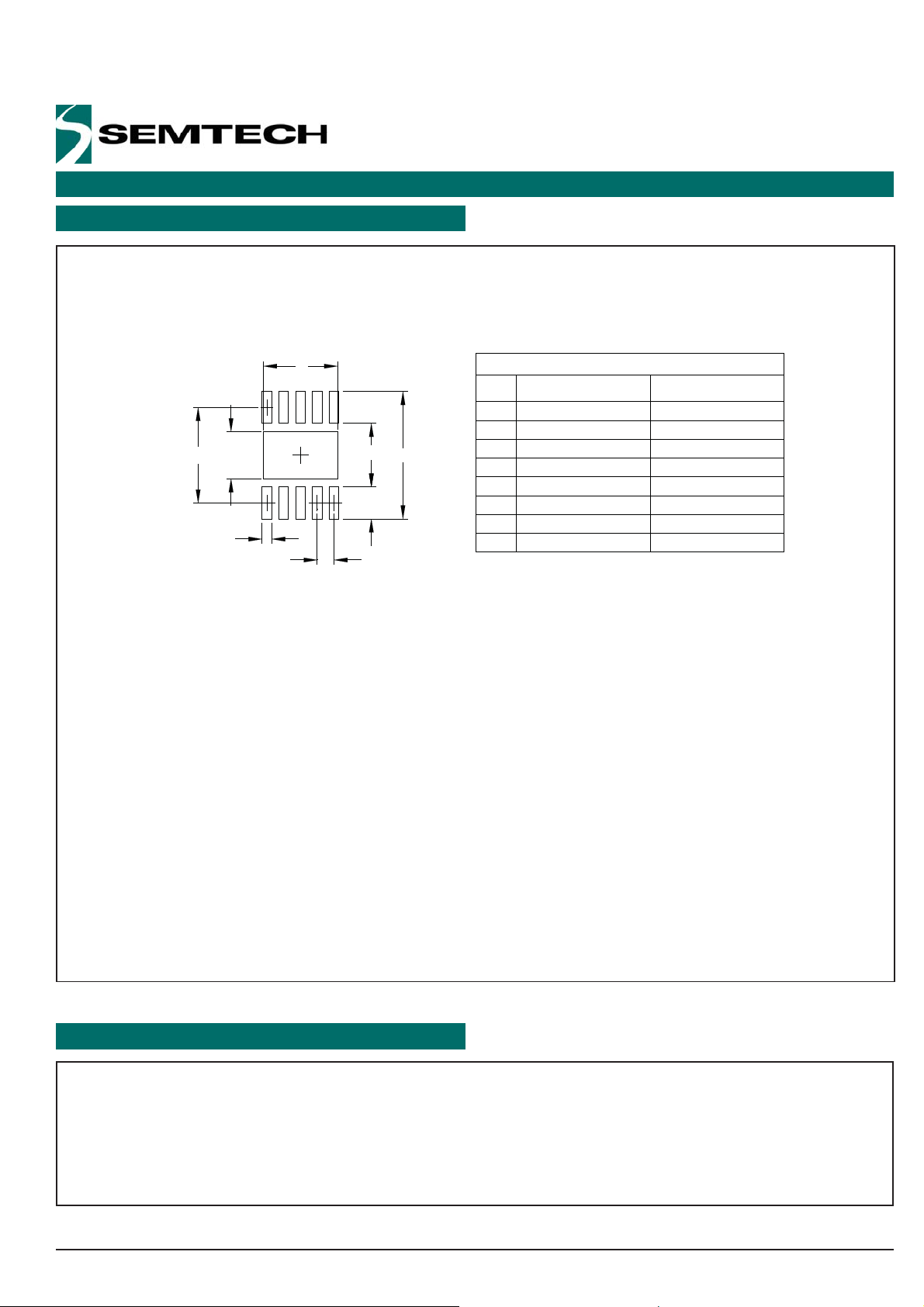
Pin Confi guration Ordering Information
egatloVtuptuOtuptuOmumixaM
morftnerruC
Am06ot0
tuptuOmumixaM
morftnerruC
Am021ot06
foegnaRdednetxE
rewoProfed
oMx5.1
sgnivaS
eciveD
V0.5X A006CS
V5.4X B006CS
V5.4X X C006CS
V0.4XXD006CS
eciveD
)1(
tuptuOegakcaP
RTSMIA006CSV0.5,Am06
01-POSM
RTSMIB006CSV5.4,Am021
RTSMIC006CSV5.4,Am06
RTSMID006CSV0.4,Am021
TRTS
MIA006CSV0.5,Am06
01-POSM
eerF-daeL
)2(
TRTSMIB006CSV5.4,Am021
TRTSMIC006CSV5.4,Am06
TRTSMID006CSV0.4,Am021
RTLMIA006CSV0.5,Am06
01-DPLM
RTLMIB006CSV5.
4,Am021
RTLMIC006CSV5.4,Am06
RTLMID006CSV0.4,Am021
TRTLMIA006CSV0.5,Am06
01-DPLM
eerF-daeL
)2(
TRTLMIB006CSV5.4,Am021
TRTLMIC006CSV5.4,Am06
TRTLMID006CSV0.4,Am021
BVE006CSehtedulcni[draoBnoitaulavE
nehwre
bmuntraptnenopmoc
]gniredro
Notes:
1) Available in Tape and Reel only. A reel contains 2500
devices for MSOP and 3000 devices for the MLPD package.
2) This product is fully WEEE and RoHS compliant.
Component Selection
MLPD
MSOP
CF1+
TOP VIEW
10
9
8
7
6
5
1
2
3
4
VOUT
VIN
CD4
CX8
CF1-
GND
CF2+
CF2-
EN

5© 2006 Semtech Corp.
www.semtech.com
POWER MANAGEMENT
SC600
Pin# Pin Name Pin Function
1 VOUT Output voltage regulated to 5.0V, 4.5V, or 4.0V.
2 CF1+ Positive terminal of bucket capacitor 1.
3 VIN Input voltage ranging from 2.5V to 6.5V.
4 CD4
Bits select the charge pump operating frequency from 8kHz, 32kHz, 262kHz, and 650kHz.
Frequency selection is defi ned in Table 1 on page 9.
5 CX8
6 EN Active high enable. Bias current is less than 1μA when set low.
7 CF2- Negative terminal of bucket capacitor 2.
8 GND Ground.
9 CF1- Negative terminal of buck capacitor 1.
10 CF2+ Positive terminal of bucket capacitor 2.
Pin Descriptions
EN
CX8
CD4
GND
VIN
6
5
4
8
3
MODE
SELECT
DRIVER S
SWITCH
BLOCK
TIMER
COMPARATORS
VIN
VOUT
VREF
CX8
CD4
VIN
CF1+
CF1-
CF2+
CF2-
VOUT
2
9
10
7
1
EN
OSC
CLK/16
CLK/8
262kHz
650kHz
X
X
X
X
A
B
X
650kHz, 262kHz, 32kHz, or 8k Hz
0
1
2
3
Block Diagram

6
© 2006 Semtech Corp. www.semtech.com
POWER MANAGEMENT
SC600
Marking Information - MLP-10
Marking Information - MSOP-10
Top Marking
600X = SC600A,B,C or D
yyww = Datecode (Example: 0552)
Bottom Marking
xxxx
xxxx
600X
yyww
600X
yyww
600X = SC600A,B,C or D
yyww = Datecode (Example: 0552)
xxxx = Semtech Lot Number

7© 2006 Semtech Corp.
www.semtech.com
POWER MANAGEMENT
SC600
Applications Information
Regulated Fractional Charge Pump Operation
A fractional charge pump is a voltage converter which
implements switched capacitor techniques to produce an
output voltage that is one of several multiples of the input
voltage. Regulated fractional charge pumps (also called
charge pump regulators) use a linear regulator with various charge pump confi gurations to deliver a regulated out-
put over a wide input voltage range. Regulated fractional
charge pumps have improved effi ciency over ordinary lin-
ear regulator and charge pump circuit combinations. The
improved effi ciency is achieved by implementing multiple
charge pump confi gurations on one integrated circuit.
The correct charge pump confi guration is automatically
selected to meet the regulation requirements at the best
possible effi ciency. The SC600 has three charge pump
confi gurations (modes), which multiply the input voltage
by 1x, 1.5x and 2x.
The charge pump confi gurations are implemented with
two switched or 'bucket' capacitors plus the input and output capacitor. The bucket capacitors are confi gured for 1x
mode at start-up to source current to the output capacitor
and bring the output up quickly. The charge pump will
begin switching in 1.5x mode. During normal operation,
starting with a fully charged Li-Ion cell, the battery voltage
will begin at about 4.1V. As the battery discharges and
the voltage decays, the SC600 will eventually transition to
2x mode when the battery voltage is approximately 3.50V.
Hysteresis is provided to prevent mode toggling. The output is prevented from exceeding 6.0V. This feature allows
the use of 6.3V ceramic capacitors.
mAhXLiFE
TM
Advantage
The plot on page 1 shows the effi ciency of the SC600A.
An example of a 5.0V regulated charge pump doubler is
plotted to demonstrate how effective the SC600’s 1.5x
mode is at improving effi ciency when the input voltage is
above 3.5V. Most of the Li-Ion battery life is above 3.5V
where the SC600 achieves more than 20% higher effi -
ciency compared to the 5.0V regulated charge pump doubler with only a 2x mode. Following the effi ciency curve
from left to right as the battery discharges, the SC600A
5.0V remains in 1.5x mode until 3.5V and then transitions
to 2x mode.
Component Versions
There are four versions of the SC600. The component
selection table on page 4 highlights the differences between the component types. The three basic differences
between the component versions are in the output voltage, maximum output current capability, and the mode
transition point.
The mode transition point is the value of input voltage at
which the component will transition between 1.5x and 2x
modes. 5.0V, 4.5V, and 4.0V versions are available. The
SC600A (5.0V) is most effi cient for applications that use
up to 60mA. The SC600B (4.5V) and SC600C (4.5V) have
different maximum output currents and mode transition
points. The lower mode transition point of the SC600C
allows it to remain in 1.5x mode longer for greater power
savings.
The SC600B has higher output capability, up to 120mA,
and S600C is rated for 60mA. The SC600D (4.0V) is for
applications using up to 120mA.
Start-Up Conditions
Typical start-up time is less than 50μs.
Caution: The SC600
must be enabled while 650kHz or 262kHz is selected to prevent over-voltage during start-up.
LED Bias and Backlighting Applications
When using the SC600 for LED bias, note that the SC600C
and SC600D require the same input power per unit of
output current even though the SC600C is more effi cient.
Also, the SC600A will have the same input power as the
SC600B though the SC600A is more effi cient.
The following plots of Input Power vs. Input Voltage highlight the differences in application of the four component
versions. To achieve the lowest possible input power, it
is desirable for the charge pump to remain in 1.5x mode
until the input voltage is as low as possible. The transition points from 1.5x to 2x are identifi ed in the plot where
the input power steps upward as the input voltage moves
lower.

8
© 2006 Semtech Corp. www.semtech.com
POWER MANAGEMENT
SC600
Applications Information (Cont.)
Input Power of SC600 A&C Output Current = 60mA Input Power of SC600 B&D Output Current = 120mA
250.00
300.00
350.00
400.00
450.00
500.00
550.00
3.003.103.203.303.403.503.603.703.803.904.004.104.20
Input Voltage[V]
Input Power[mW]
SC600A 5.0V & SC600B 4.5V
SC600C 4.5 V & SC600D 4.0V
Input Voltage[V]
500.00
550.00
600.00
650.00
700.00
750.00
800.00
850.00
900.00
950.00
1000.00
3.003.103.203.303.403.503.603.703.803.904.004.104.20
Input Vol tage[V ]
Input Power[mW]
SC600B 4.5V
SC600D 4.0V

9© 2006 Semtech Corp.
www.semtech.com
POWER MANAGEMENT
SC600
Applications Information (Cont.)
Brightness Control with PWM Input
Brightness control using a PWM input can be achieved
with the application circuit below. Note that by connecting
CX8 to the PWM signal the switching frequency is changed
as the PWM signal changes. The charge pump operates
at 262kHz during the on-time when there is a demand for
current, and then changes to 32kHz when there is no load
current. This is done to save battery power by taking advantage of the lower 280μA quiescent current at 32kHz.
The ripple voltage seen at the output is reasonable for
LED applications, but the output capacitance can be increased to reduce the ripple if required. The sum of the
LED currents for this circuit is 55mA during the on-time.
White LED Driver Circuit with PWM Brightness Control
Voltage Waveforms for LED Driver Circuit
Cin
1uF
2.7V to 6.5V
Cbucket1
1uF
Cbucket2
1uF
VIN
EN
CD4
CX8
GND
CF2-
CF2+
CF1-
CF1+
VOUT
3
6
4
5
8
7
10
9
2
1
U1
Cout
1uF
PWM
S
C
6
0
0
A
100
100 10 0
5.0V
Ripple Voltage vs. Input Voltage
0
50
100
150
200
250
300
350
400
450
500
2.8 3.3 3.8 4.3 4.8 5.3 5.8
Input Voltag e [V]
Ripple Voltage [mV]
Vout p-p
Vin p -p
Battery Current vs. Input Voltage
for Various Duty Cycles
0
20
40
60
80
100
120
2.833.23.43.63.84
Input Voltage [V]
Battery Current [mA]
89.20%
70.30%
50.20%
30.20%

10
© 2006 Semtech Corp. www.semtech.com
POWER MANAGEMENT
SC600
Applications Information (Cont.)
Comparison with Other Regulation Methods
In many instances, a charge pump regulator is the best
choice for portable power applications. These regulators
offer many advantages over switch mode regulators. A
smaller bill of materials, less layout area, lower component height, less noise, no EMF, and less overall circuit
cost are typical reasons to use this type of regulation. In
some cases the effi ciency of a charge pump regulator ex-
ceeds the effi ciency of a switch mode regulator.
Inductors are often the largest and most expensive discrete component in a design. Because there are no inductors used in the SC600, cost, noise, layout area, as
well as the the EMF associated with the inductor, are
eliminated.
The SC600’s fi xed frequency harmonics are an advantage
in portable communications equipment, such as cellular
telephones. The SC600 has distinct frequencies of operation, so the harmonics are predictable. The harmonics
are not fi xed in a switch mode regulator.
Ripple Performance
Examples of the output ripple, charge pump frequency
and capacitor size are listed in Table 2.
Switch mode regulators have harmonics which vary due to
the pulse width modulation used to regulate the output.
Varying harmonics can make it diffi cult to ensure accept-
able noise performance over the entire operating range.
Many switch mode regulators have increased voltage ripple on the output during pulse skipping mode due to large
periods of time when no current is supplied to the output.
The SC600 supplies current to the output continuously,
so the voltage ripple is less than a switch mode regulator, even with greatly reduced output capacitance. The
SC600 delivers a continuous current to the output during
1x, 1.5x and 2x modes. Most of the battery life requires
1.5x mode.
Frequency Selection
CX8 and CD4 are frequency select inputs; input from a µP
or other device may be used to change the charge pump
frequency at any time (as shown in Table 1). The optimal frequency will depend upon the capacitor values, the
load current, and the acceptable amount of output ripple.
Lower frequencies will be more effi cient, while higher fre-
quencies will support higher output currents with lower
ripple.
ycneuqerFgnihctiwS8XC4DC
zHk2300
zHk801
zHk26210
zHk05611
Table 1 -Frequency Selection Logic
.oNtraP]zHk[.qerFI
TUO
]Am[]p-pVm[elppiRtuptuO
edomx5.1
]p-pVm[elppiRtupuO
edomx2
C
TUO
]Fμ[C
TEKCUB
]Fμ[
V0.5A006CS 85 565111
23020515211
26206520211
05606015111
05606025233.01
Table 2 -Ripple Performance

11© 2006 Semtech Corp.
www.semtech.com
POWER MANAGEMENT
SC600
Applications Information (Cont.)
Mode Transition Impedance
The mode transition impedance Ro refers to the output
resistance of the charge pump before a transition to a
stronger mode occurs. Ro is dependent upon the fractional charge pump, switching frequency, bucket capacitor value, bucket capacitor ESR, and the internal switch
resistances.
Ro is proportional to,
1
fC
Ro can be measured to verify a low transition impedance. Before measuring Ro, select the capacitors, set
the operating frequency and a constant load current. Find
the input voltage just before a weak to strong mode transition (i.e., 1.5x to 2x mode). Measure VIN, V
OUT
, and I
OUT
before the transition.
Ro will be,
Ro=
mode V
IN
V
OUT
I
OUT
Table 2 -Ripple Performance (Cont.)
.oNtraP]zHk[.qerFI
TUO
]Am[]p-pVm[elppiRtuptuO
edomx5.1
]p-pVm[elppiRtupuO
edomx2
C
TUO
]Fμ[C
TEKCUB
]Fμ[
B006CS
)1(
V5.4 8015120511
23040030911
262021045211
056021515211
056021035433.01
V0.4D006CS 8015010511
23040425411
262021030211
056021110211
056021520433.01
Note: (1) SC600C is very similar to SC600B.
A lower value of Ro will improve efficiency, so low ESR
ceramic capacitors are required. An X7R or X5R dielectric is recommended. Y5V dielectric can require 2 to 3
times the rated value of an X7R dielectric for the same
performance over the operating temperature range.
Efficiency
Efficiency for the SC600 is defined as,
η =
VOI
O
V
IN
mode I
O
I
Q

12
© 2006 Semtech Corp. www.semtech.com
POWER MANAGEMENT
SC600
Applications Information (Cont.)
where:
V
O
= output voltage
I
O
= output currrent
mode = 1.5x or 2x
V
IN
= input voltage
I
Q
= quiescent current
(from Electrical Characteristics on page 2)
The mode may be identifi ed by measuring input current
and output current and calculating as mode = IIN/I
OUT
.
Alternately, the mode can be identifi ed by identifying
the voltage at the bucket capacitor, CF1 with an
oscilloscope.
Calculating Power Dissipation
The power dissipated by the SC600 is calculated as,
P
D
= PIN - P
OUT
PD = VIN · (mode IO + IQ) - VO · I
O
Suggested Capacitors
The following is a short list of some of the manufacturers
and types of multi-layer ceramic capacitors that are suggested for the SC600.
Short-Circuit and Over-Temperature Protection
The output current is limited to 600mA to protect against
short-circuit conditions. Over-temperature protection is
also provided.
Design and Layout Considerations
The layout example on page 15 uses the 1206 case size
for the capacitors, so a smaller layout area is possible.
The bucket capacitors and the SC600 are on the same
side of the card. To minimize trace inductance, traces are
short and wide with no vias to the bucket capacitors. The
input and output caps are on the bottom side directly under the SC600 and vias are used to connect directly to
copper shapes used for the input and output. The input
and output capacitors and Pin 8 should be connected to
ground very near the SC600.
rerutcafunaMrebmuNtraP]Fμ[ecnaticapaCepyTcirtceleiDeziSegakcaPAIEegatloV
gnitaR
XVAK522CZ50802.2R7X5080V01
XVAK501C
Z50800.1R7X5080V01
XVAK433CZ508033.0R7X5080V01
cinosanaPK522J0BY2JCE2.2R5X5080V3.6
cinosanaP501A1BY2JCE0.1R7X5080V01
cinosan
aPK501J0BV1JCE0.1R5X2040V3.6
cinosanaPK433J0BV1JCE33.0R5X3060V3.6
KDT501A1R5X8061C0.1R5X3060V01
KDTZ601A1V5Y2021C0.1R5X5080V
01
KDTk433A1R5X8061C33.0R5X3060V01

13© 2006 Semtech Corp.
www.semtech.com
POWER MANAGEMENT
SC600
Typical Characteristics
Load Regulation, V
IN
= 3.6V, Freq. = 650kHz Line Regulation, Freq. = 650kHz
Effi ciency vs. Output Current, V
IN
= 3.6V,
Freq. = 650kHz
Start-Up Conditions for 5.0V Output
Ripple Voltage Start-Up Conditions for 4.0V Output
3.8
4
4.2
4.4
4.6
4.8
5
5.2
0 20 40 60 80 100 120
Load Current [mA]
Output Voltage [V]
SC600A at 60mA
SC600B at 120mA
SC600D at 120mA
3.8
4
4.2
4.4
4.6
4.8
5
2.5 3 3.5 4 4.5 5 5.5 6 6.5
Input Voltage [V]
Output Voltage [V]
SC600A at 60mA
SC600B at 120mA
SC600D at 120mA
50
55
60
65
70
75
80
85
90
95
0 102030405060708090100110120
Current [mA]
Efficiency [%]
SC600A 5.0V
SC600B 4.5V
SC600C 4.5V
SC600D 4.0V

14
© 2006 Semtech Corp. www.semtech.com
POWER MANAGEMENT
SC600
Typical Characteristics (Cont.)
Evaluation Board Schematic
Evaluation Board Bill of Materials
Reference Value Comment
U1 SC600 MSOP-10 or MLPD-10 lead 3x3mm
C1, C2, C3, C4 1.0µF Ceramic, low ESR type
C5 10µF This extra capacitor supports usage of long power leads from a benchtop supply
R7, R8, R9 - Add limiting resistors to meet the requirements of the application
D1, D2, D3 - Add white or blue LEDs to meet the requirements of the applicaton on SMT pads
D4, D5, D6 - Add white or blue LEDs to meet the requirements of the application on PTH pads
60
65
70
75
80
85
90
95
3.03.23.43.63.84.04.2
Input Voltage [V]
Efficiency [%]
SC600B 4.5V@120mA
SC600C 4.5V@60mA
60
65
70
75
80
85
90
95
3.03.23.43.63.84.04.2
Input Voltage [V]
Efficiency [%]
SC600A 5.0V@60mA
SC600D 4.0V@120mA
Effi ciency vs. Input Voltage for B and C Version Effi ciency vs. Input Voltage for A and D Version

15© 2006 Semtech Corp.
www.semtech.com
POWER MANAGEMENT
SC600
Evaluation Board Gerber Plots
Top View Bottom View

16
© 2006 Semtech Corp. www.semtech.com
POWER MANAGEMENT
SC600
Outline Drawing - MSOP-10
bbb C A-B D
DIMENSIONS "E1" AND "D" DO NOT INCLUDE MOLD FLASH, PROTRUSIONS
3.
OR GATE BURRS.
DATUMS AND TO BE DETERMINED AT DATUM PLANE
CONTROLLING DIMENSIONS ARE IN MILLIMETERS (ANGLES IN DEGREES).
-B-
NOTES:
1.
2.
-A- -H-
SIDE VIEW
A
B
C
D
H
PLANE
0°
.010
.004
-
.016
.003
.024
(.037)
-
.000
.030
---
-
0.25
0.10
8° 0°
-
8°
0.60
(.95)
.032
.009
0.40
0.08
.043
.006
.037 0.75
0.00
-
0.80
0.23
-
0.95
1.10
0.15
-
-
-
e
.193 BSC
.020 BSC
DETAIL
aaa
C
SEATING
INDICATOR
ccc
C
2X N/2 TIPS
PIN 1
2X
E/2
10
SEE DETAIL
A1
A
A2
bxN
D
0.25
A
PLANE
GAGE
.003
E1
12
N
.114
.114
.118
.118
.007
-
10
01
c
(L1)
L
A
0.08
3.00
3.00
4.90 BSC
0.50 BSC
.122
.122
2.90
2.90
.011 0.17
3.10
3.10
0.27
-
REFERENCE JEDEC STD MO-187, VARIATION BA.
4.
DIM
ccc
A1
e
bbb
aaa
01
L1
N
L
D
E1
E
A2
b
c
A
MILLIMETERS
NOM
INCHES
DIMENSIONS
MIN NOM MAX MIN MAX
E

17© 2006 Semtech Corp.
www.semtech.com
POWER MANAGEMENT
SC600
Land Pattern - MSOP-10
THIS LAND PATTERN IS FOR REFERENCE PURPOSES ONLY.
CONSULT YOUR MANUFACTURING GROUP TO ENSURE YOUR
COMPANY'S MANUFACTURING GUIDELINES ARE MET.
NOTES:
1.
P
(C)
X
Z
G
Y
.063
.224
.011
.020
.098
(.161)
5.70
1.60
0.30
0.50
2.50
(4.10)
MILLIMETERS
DIMENSIONS
DIM INCHES
Y
Z
G
P
X
C

18
© 2006 Semtech Corp. www.semtech.com
POWER MANAGEMENT
SC600
Outline Drawing - MLPD-10
MIN
aaa
bbb
b
e
L
N
D
C
E
A1
A2
A
DIM
MILLIMETERS
NOM
DIMENSIONS
MAXNOM
INCHES
MIN MAX
.114
.118
.122
2.90 3.00 3.10
-
-
-
-
(LASER MARK)
INDICATOR
PIN 1
1N2
NOTES:
CONTROLLING DIMENSIONS ARE IN MILLIMETERS (ANGLES IN DEGREES).
COPLANARITY APPLIES TO THE EXPOSED PAD AS WELL AS TERMINALS.
2.
1.
.003
.007
.042
10
.009
.048
-
.000
.031
(.008)
0.08
0.23
10
.011
.052
0.18
1.06
.039
-
.002-0.00
0.80
1.31
0.30
1.21
-
0.05
1.00
(0.20)
.004 0.10
0.50 BSC.020 BSC
0.30.012 .020.016 0.40 0.50
A
aaa
C
A2
SEATING
PLANE
A1
A
bxN
bbb C A B
B
e
C
C
D
LxN
E
E
.074 .079 .083 1.87 2.02
2.12
19© 2006 Semtech Corp.
www.semtech.com
POWER MANAGEMENT
SC600
Land Pattern - MLPD-10
.087
.055
2.20
1.40
.150
.020
.012
.037
3.80
0.30
0.95
0.50
(.112)
.075 1.90
(2.85)
K
H
X
THIS LAND PATTERN IS FOR REFERENCE PURPOSES ONLY.
CONSULT YOUR MANUFACTURING GROUP TO ENSURE YOUR
COMPANY'S MANUFACTURING GUIDELINES ARE MET.
NOTES:
1.
INCHES
DIMENSIONS
G
K
H
X
Y
P
Z
C
DIM MILLIMETERS
Y
Z
G
(C)
P
www.semtech.com
Semtech Corporation
Power Management Products Division
200 Flynn Road, Camarillo, CA 93012
Phone: (805) 498-2111 FAX (805) 498-3804
Contact Information
 Loading...