


POWER MANAGEMENT
R2
R3
L1
Q1
D1
C2
C1
R4
VIN
VOUT
GND
D2
optional
U2
SC2603
VIN
5
EN/SS
3
FB
1
GND
2
CS
6
Gate
4
R1
C4
Enable
C3
R5
C5
(open collector)
Open Drain with < 100Ω
pull down impedance
SC2603
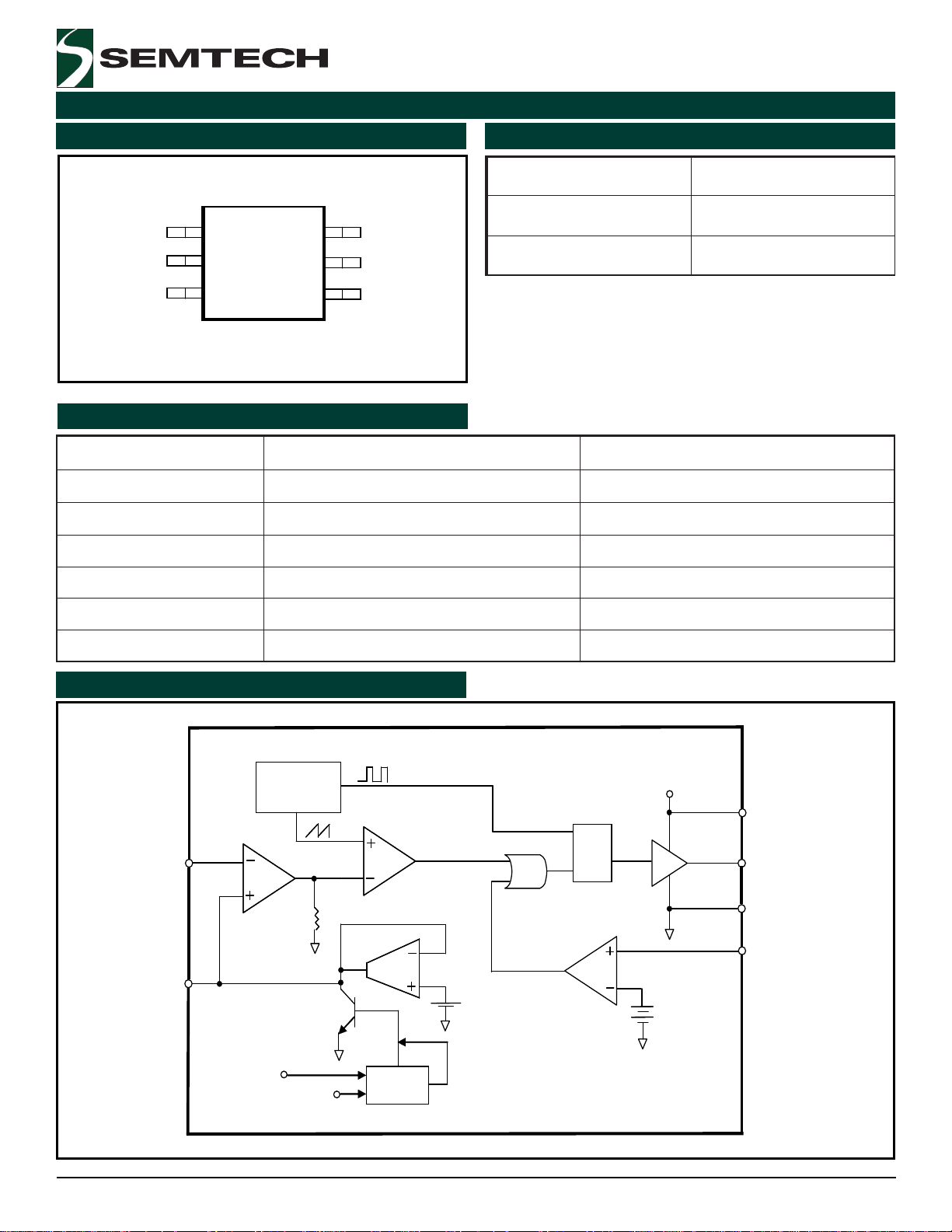
Simple PWM Boost Controller
Description
The SC2603 is a versatile, low-cost, voltage-mode PWM
controller designed for 16V input DC/DC power supply
applications. A simple, fixed-voltage boost regulator can
be implemented using the SC2603 with a minimum of
external components. The small device footprint
allows for compact circuit design.
SC2603 features include a temperature compensated
voltage reference, triangle wave oscillator, current limit
comparator, frequency shift over-current protection, and
an internally compensated error amplifier. Pulse by pulse
current limiting is implemented by sensing the
differential voltage across an external resistor, or an
appropriately sized PC board trace.
The SC2603 operates at a fixed frequency of 200kHz,
providing an optimum compromise between efficiency,
external component size, and cost.
Typical Application Circuit
Features
u Low cost / small size
u Switch mode efficiency up to 95%
u 1% reference voltage accuracy
u Over-current protection
u 800mA output drive
u 5V to 16V input power source
u No need for external compensation network
u SOT23-6 is fully WEEE and RoHS compliant
Applications
u Portable Devices
u Flat Panel TV
u TV Set Top Box
u Auxiliary Supplies
u Peripheral Card Supplies
u Industrial Power Supplies
u High Density DC/DC Conversion
Revision: Nov 14, 2006
1
www.semtech.com

SC2603
retemaraP slobmyS snoitidnoC niM pyT xaM stinU
ecnerefeR V
FER
522.1 052.1 572.1 V
tnerruCsaiBkcabdeeF I
BF
VBFV=
SS/NE
V,
NI
V21= 0.2 0.8 Aµ
tnerruCtnecseiuQ I
Q
VotnitnerruC
NI
nip 0.5 0.8 Am
noitalugeRdaoL V
O
I;V52=
O
A1otA1.0= 5.0 0.1 %
noitalugeReniL V
NI
V;V51otV5=
O
I;V52=
O
Am001= 4.1 2 %
dlohserhTtimiLtnerruC SC 86 37 87 Vm
ycneuqerFrotallicsO T
A
52=OC 091 002 012 zHk
tfihSycneuqerFrotallicsO V
BF
V<
FER
2/ 05 zHk
elcyCytuDxaM 09 59 %
dlohserhTOLVU V
OLVU
V
NI
pugnipmar 2.4 5.4 V
siseretsyHOLVU 004 Vm
tnerruCecruoSrevirD I
ECRUOS
V
NI
C,V21=
ETAG
Fn01= 5.0 8.0 1.1 A
tnerruCkniSrevirD I
KNIS
V
NI
C,V21=
ETAG
Fn01= 5.0 8.0 1.1 A
tnerruCegrahCtratStfoS I
SS
06 Aµ
kaePpmaRlanretnI V
KAEP_R
4.1 V
yellaVpmaRlanretnI V
YELLAV_R
4.0 V
dlohserhTelbanE V
NE_HT
levelsihtwolebnwodlluP
tuptuoehtelbasidot
90.0 21.0 V
retemaraP lobmyS mumixaM stinU
egatloVtupnI V
NI
DNGot 02ot3.0- V
egnaRerutarepmeTegarotS T
GTS
051+ot54- C°
erutarepmeTnoitcnuJmumixaM T
J
051 C°
.ceS01)gniredloS(erutarepmeTdaeL T
DAEL
003 C°
tneibmAotnoitcnuJ,ecnatsiseRlamrehT
)1(
θ
AJ
561 W/C°
esaCotnoitcnuJ,ecnatsiseRlamrehT
θ
CJ
201 W/C°
egrahcsiDegruSlacirtcelE
)2(
DSE 2 VK
POWER MANAGEMENT
Absolute Maximum Ratings
Exceeding the specifications below may result in permanent damage to the device, or device malfunction. Operation outside of the parameters specified
in the Electrical Characteristics section is not implied.
Note:
(1) Mounting pad has to be larger than one square inch on two sided printed circuit board with minimum 1 ounce copper
(2) Human model.
Electrical Characteristics
VIN= 12V; VO = 25V; TA = TJ = -40°C to 125°C unless otherwise specified.
2 2005 Semtech Corp.
www.semtech.com
POWER MANAGEMENT
srebmuNtraP egakcaP
TRTKS3062CS
1( () )2
6-32TOS
BVE3062CS
#niP emaNniP noitcnuFniP
1 BF .)-(tupnireifilpmarorrE
2 DNG .dnuorgeciveD
3 SS/NE .niPtratStfoS/elbanE
4 etaG .tuptuorevirdetaG
5 NIV .egatloVtupnIeciveD
6 SC .tupnIesneStnerruC
2
1
3
FB
GND
EN/SS
4
6
CS
5
VIN
GATE
SOT23-6
VIN
FB
Gate
CS
UVLO
GND
PWM
EN/SS
70mV
Current
Limit
VIN
UV
S
Q
R
OSCILLATOROSCILLATOR
1.25V
REF
1.25V
REF
25K
SC2603
Pin Configuration
Pin Descriptions
Ordering Information
Top View
Note:
(1) Only available in tape and reel packaging. A reel
contains 3000 devices.
(2) Lead free product. This product is fully WEEE and
RoHS compliant
Block Diagram
2005 Semtech Corp.
3
www.semtech.com
POWER MANAGEMENT
−= 1
25.1
21
OUT
V
RR
VOUT
R2
R1
FB
1
SC2603
SC2603
Theory of Operation
The SC2603 is a versatile, low-cost, voltage-mode PWM
controller designed for DC/DC power supply applications.
In normal condition, the SC2603 operats at a fixed
200KHz. One exception is that when the FB pin voltage
drops to one half, the frequency will be shifted to one
fouth of 200KHz.
SC2603 features include a temperature compensated
voltage reference, triangle wave oscillator, current limit
comparator, frequency shift over-current protection, and
an internally compensated error amplifier. Pulse by pulse
current limiting is implemented by sensing the
differential voltage across an external resistor, or an
appropriately sized PC board trace.
Application Information
Soft-Start
Soft-start prevents a DC-DC converter from drawing
excessive current from the power source during start up.
If the soft-start time is made sufficiently long, then the
output will enter regulation without overshoot. An external
capacitor is connected from the EN/SS pin to the ground.
After the part’s input voltage surpasses the UVLO, the
EN/SS pin is allowed to charge its capacitor with 60µA.
When 100mV is reached at the EN/SS pin, the internal
comp node is at 0.4V. The SC2603 will start switching,
and the converter output comes into regulation. Because
the FB pin voltage follows EN/SS pin voltage, finally, the
EN/SS pin voltage will be clamped at 1.25V same as the
refernece voltage.
Setting the Output Voltage
An external resistive divider R1 and R2 with its center
tap tied to the FB pin sets the output voltage.
Under Voltage Lockout
The under voltage lockout circuit of the SC2603 assures
that the gate driver output remains in the off state whenever the supply voltage drops below set parameters. Lockout occurs if VIN falls below 3.8V. Normal operation resumes once V
rises above 4.2V.
IN
4 2005 Semtech Corp.
www.semtech.com

POWER MANAGEMENT
PEAKS
ImVR /70=
V
IN
V
OUT
I
OUT
I
IN
t0
t1
t2 t3
t4
Application Information
Over Current Protection
The over-current protection is implemented by a sensing
resistor and an internal current-limit comparator with a
threshold of 70mV. If the switching current through the
sensing resistor causing voltage to drop at the CS pin
reachs 70mV, the SC2603 will immediately turn the gate
pulse off to limit the current through the power switch.
The figure below shows over-current waveforms. At t1,
the input current IIN begins to increase as the load I
builds up until it hits the OCP threshold at t2. At t2, V
begins to drop as I
starts increasing toward t3 while V
OUT
and IIN remain the same. At t3, there two events are
happening. 1) V
is at half of its regulating voltage. At
OUT
this point, the internal oscillator runs into frequency shift
mode and shifts the frequency to one fourth of the operating frequency. 2) The diode starts conducting current
without limit causing V
Finally, V
and V
IN
OUT
to fall due to supply current limit.
IN
both drops to zero and I
becomes the
IN
input supply current limit.
OUT
OUT
SC2603
IN
A RC filter at the CS pin is necessary to filter out noise to
ensure accurate sensing.
The value of the sensing resistor can be caculated by
the following equation:
Where I
MOSFET.
is the input peak current through the power
PEAK
2005 Semtech Corp.
Over Current Waveforms
5
www.semtech.com

POWER MANAGEMENT
Applications Information
Layout Guidelines
SC2603
Careful attention to layout requirements are necessary
for successful implementation of the SC2603 PWM controller. High currents switching at 200kHz are present in
the application and their effect on ground plane voltage
differentials must be understood and minimized.
1) The high power parts of the circuit should be laid out
first. A ground plane should be used, the number and
position of ground plane interruptions should be such as
to not unnecessarily compromise ground plane integrity.
Isolated or semi-isolated areas of the ground plane may
be deliberately introduced to constrain ground currents
to particular areas, for example the input capacitor and
bottom Schottky ground.
2) The loop formed by the output Capacitor(s) (Cout), the
FET (Q1), the current sensing resistor, and the Schottky
(D1) must be kept as small as possible. This loop contains all the high current, fast transition switching. Connections should be as wide and as short as possible to
minimize loop inductance. Minimizing this loop area will
reduce EMI, lower ground injection currents, resulting in
electrically “cleaner” grounds for the rest of the system
and minimize source ringing, resulting in more reliable
gate switching signals.
5) The SC2603 is best placed over an isolated ground
plane area. The soft-start capacitor, the VIN decoupling
capacitor, and the current sensing filter capacitor should
also connected to this ground pad area. This isolated
ground area should be connected to the main ground by
a trace that runs from the GND pin to the ground side of
the output capacitor. If this is not possible, the GND pin
may be connected to the ground path between the Output Capacitor and the Cin, Q1, D1 loop. Under no circumstances should GND be returned to a ground inside
the Cin, Q1, D1 loop.
6) Input voltage of the SC2603 should be supplied from
the power rail through a 2.2~10Ω resistor, the V
should be decoupled directly to GND by a 0.1µF~1µf
ceramic capacitor, trace lengths should be as short as
possible.
7) An RC low pass filter is required to filter out leading
edge current spikes on the current sensing resistor. The
filter capacitor needs to be very close to the CS and
GND to reduce noise pickup.
IN
pin
3) The connection between the junction of Q1, D1 and
the output capacitor should be a wide trace or copper
region. It should be as short as practical. Since this connection has fast voltage transitions, keeping this connection short will minimize EMI.
4) The Output Capacitor(s) (Cout) should be located as
close to the load as possible, fast transient load currents are supplied by Cout only, and connections between Cout and the load must be short, wide copper
areas to minimize inductance and resistance.
6 2005 Semtech Corp.
www.semtech.com

POWER MANAGEMENT
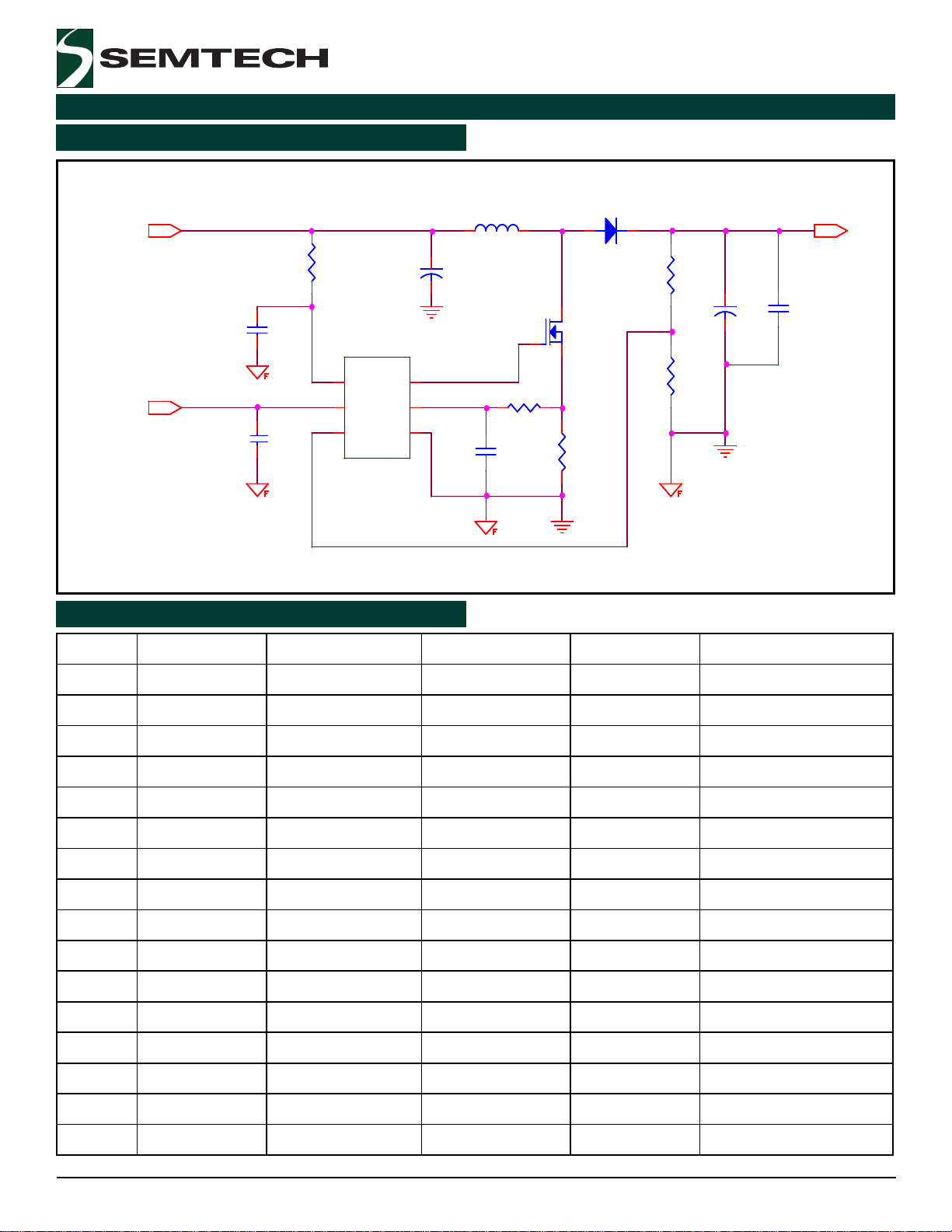
Vout
12VIN
+
Cout
2.2
0.1uF
Q1
0.1uF
D1
SC2603
GND
1
VIN
5
3
CS
6
Gate
2
FB
4
Rb
Ra
Rs
EN/SS
20uH
Cin
Heavy lines indicate the critical loop carrying high pulsating current.
The inductance of this loop needs to be minimized.
Applications Information (Cont.)
Layout diagram for the SC2603
SC2603
2005 Semtech Corp.
7
www.semtech.com
POWER MANAGEMENT
R2
34K
R4
1.78K
L1
18uH
Q1
AO4442
D1
3A, 40V
C2
330u/35V
C1
470u
R5
1K
VIN = 12V
VOUT=25V
U2
SC2603
VIN
5
EN/SS
3
FB1GND
2
CS
6
Gate
4
C11
1u
R1
2.2
C4
0.1u
Enable
C3
1u
R6
20m
C5
120p
(open drain)
R2
34K
R4
1.78K
L1
18uH
Q1
AO4442
D1
3A, 40V
C2
330u/35V
C1
470u
R5
1K
VIN = 12V
VOUT=25V
U2
SC2603
VIN
5
EN/SS
3
FB1GND
2
CS
6
Gate
4
C11
1u
R1
2.2
C4
0.1u
Enable
C3
1u
R6
20m
C5
120p
(open drain)
Open Drain with < 100Ω
pull down impedance
SEMTECHSOT23-6SC2603U1116
20mR6115
6031KR5114
6031.78KR4113
6030R3112
60334KR2111
6032.2R1110
Alpha & OmegaAO4442Q119
COOPER18uHL118
1N5819D117
8051uC1116
603120pC515
6030.1uC414
6031uFC313
SANYO330u/AlumC212
SANYO470u/AlumC111
VendorfootprintPartReferenceQuantityItem
SEMTECHSOT23-6SC2603U1116
20mR6115
6031KR5114
6031.78KR4113
6030R3112
60334KR2111
6032.2R1110
Alpha & OmegaAO4442Q119
COOPER18uHL118
1N5819D117
8051uC1116
603120pC515
6030.1uC414
6031uFC313
SANYO330u/AlumC212
SANYO470u/AlumC111
VendorfootprintPartReferenceQuantityItem
Applications Circuit
12V to 25V @ 1A boost converter
SC2603
Bill of Material
8 2005 Semtech Corp.
www.semtech.com

POWER MANAGEMENT
-10
-5
0
5
10
15
20
25
30
35
40
100.0E+0 1.0E+3 10.0E+3 100.0E+3 1.0E+6 10.0E+6
Frequency (Hz)
Gain (dB)
-45
0
45
90
135
180
Phase (deg)
Gain
Phase
23.000
23.500
24.000
24.500
25.000
25.500
26.000
4 6 8 10 12 14 16
Input Voltage - (V )
Output Voltage - (V)
23
23.5
24
24.5
25
25.5
26
0.0 0.1 0.2 0.3 0.4 0.5 0.6 0.7 0.8 0.9 1.0 1.1
Output Current - (A)
Output Voltage - (V)
80
82
84
86
88
90
92
94
96
98
0 0.1 0.2 0.3 0.4 0.5 0.6 0.7 0.8 0.9 1 1.1
Output Current - (A)
Efficiency - (%)
24.2
24.4
24.6
24.8
25
25.2
25.4
25.6
0 0.5 1 1.5 2 2.5 3
Output Current - (A)
Output Voltage - (A)
Typical Characteristics
SC2603
Error Amplifier: Gain and Phase
Efficiency (VIN = 12V, VO = 25V)
Load Regulation (V
= 12V, VO = 25V)
IN
Line Regulation (VO = 25V, IO = 1A)
OCP (VIN = 12V, VO = 25V)
2005 Semtech Corp.
Frequency Shift (V
9
vs. FSW)
FB
www.semtech.com
POWER MANAGEMENT
1.22
1.225
1.23
1.235
1.24
1.245
1.25
1.255
1.26
-50 -25 0 25 50 75 100 125 150
TEMPERATURE
(
o
C
)
REFERENCE VOLTAGE
(
V
)
180
185
190
195
200
205
210
-50 -25 0 25 50 7 5 100 125 150
TEM PERATURE (OC)
OSCILLATOR FREQUENCY
(kHz)
4. 05
4. 08
4. 10
4. 13
4. 15
4. 18
4. 20
4. 23
4. 25
4. 28
4. 30
-50 - 25 0 25 5 0 7 5 100 12 5 1 50
TEMPERA T U R E (OC)
UVLO THRESHOLD (V)
0.15
0.2
0.25
0.3
0.35
0.4
0.45
0.5
0.55
-50 0 50 100 15 0
TEM P E R ATURE (OC)
UVLO HYSTERESIS (V)
68
69
70
71
72
73
74
75
-50 -25 0 25 50 75 100 125 150
TEMPERATURE (OC)
CURRENT LIMIT THRESHOLD (mV)
Typical Characteristics
SC2603
Reference Voltage vs Temperature
VIN=12V
VIN=5V
Oscillator Frequency vs Temperature
UVLO Hysteresis vs Temperature
Current Limit Threshold vs Temperature
UVLO Threshold vs Temperature
10 2005 Semtech Corp.
www.semtech.com
POWER MANAGEMENT
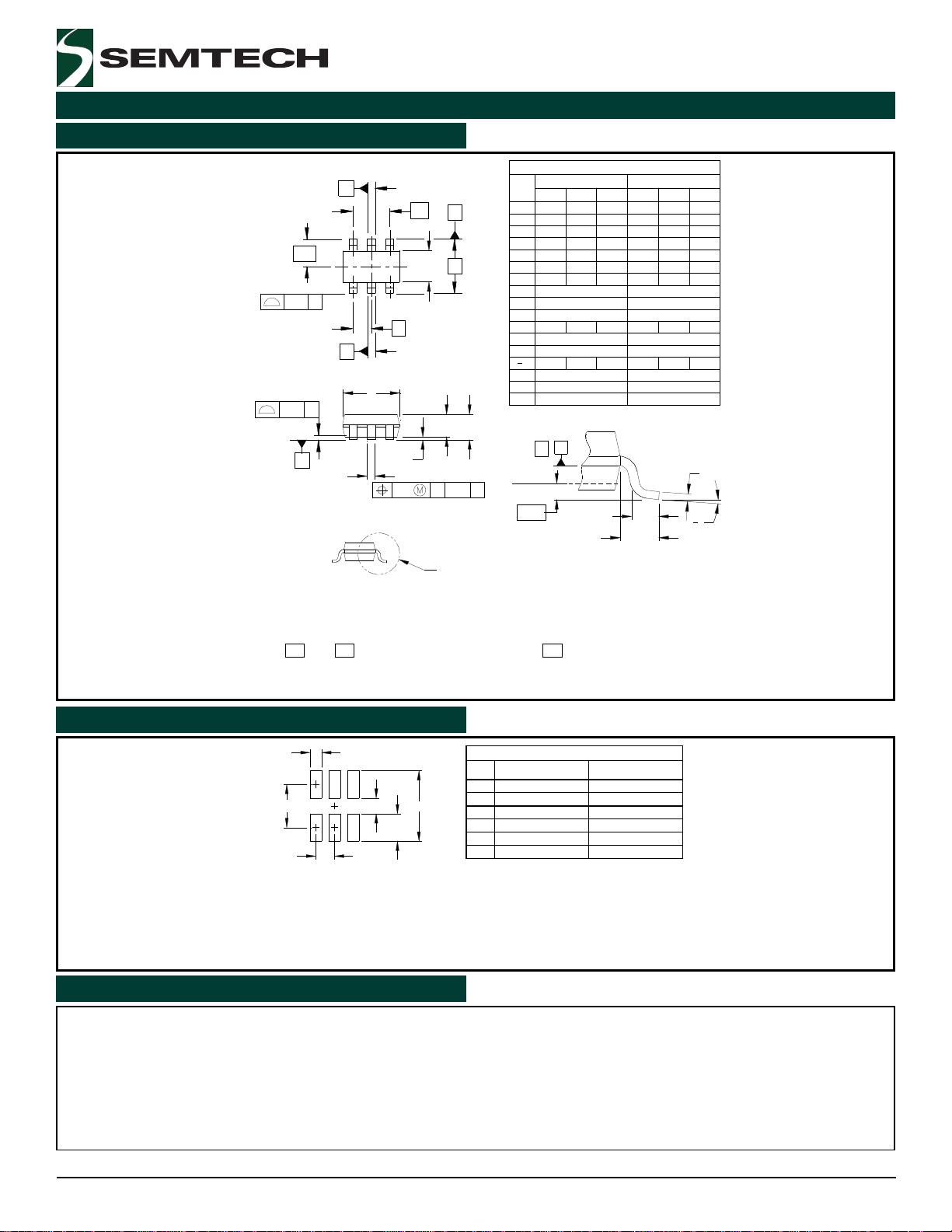
.110 BSC
.037 BSC
DETAIL
aaa
C
SEATING
ccc
C
2X N/2 TIPS
2X E/2
6
SEE DETAIL
A1
A
A2
bxN
A
.008
1 2
N
E
.060
.114
.063
.118
.010
-
6
A
0.20
1.60
3.00
2.80 BSC
0.95 BSC
.069 1.50
2.90
.020 0.25
1.75
0.50
-
EI
L
(L1)
c
01
0.25
PLANE
GAGE
H
2.80.110
bbb
C
A-B
D
0°
.008
-
.004
.012
.003
(.024)
.018
-
.035
.000
.035
-
-
.045
0.10
0.20
10° 0°
-
10°
1.15
(0.60)
0.45.024
.009
0.30
0.08
.057
.051
.006 0.00
.90
0.90
0.22
0.60
-
0.15
1.45
1.30
-
-
1.90 BSC.075 BSC
A
e1
D
e
B
C
H
NOM
INCHES
DIMENSIONS
L1
aaa
bbb
ccc
01
N
DIM
c
e
e1
L
E1
E
D
A1
A2
b
A
MIN
MILLIMETERS
MAX MIN NOM MAX
PLANE
D
DATUMS AND TO BE DETERMINED AT DATUM PLANE
CONTROLLING DIMENSIONS ARE IN MILLIMETERS (ANGLES IN DEGREES).
DIMENSIONS "E1" AND "D" DO NOT INCLUDE MOLD FLASH, PROTRUSIONS3.
OR GATE BURRS.
NOTES:
1.
2. -A-
-B-
-H-
SIDE VIEW
THIS LAND PATTERN IS FOR REFERENCE PURPOSES ONLY.
CONSULT YOUR MANUFACTURING GROUP TO ENSURE YOUR
COMPANY'S MANUFACTURING GUIDELINES ARE MET.
NOTES:
1.
DIMENSIONS
INCHES
Y
Z
DIM
G
P
X
C
MILLIMETERS
P
(C)
Z
Y
G
.043
.141
.055
(.098)
.037
.024
1.40
(2.50)
0.95
0.60
1.10
3.60
X
DIMENSIONS
INCHES
Y
Z
DIM
G
P
X
C
MILLIMETERS
Outline Drawing - SOT23-6
SC2603
Land Pattern - SOT23-6
Contact Information
2005 Semtech Corp.
Phone: (805)498-2111 FAX (805)498-3804
Power Management Products Division
200 Flynn Road, Camarillo, CA 93012
Semtech Corporation
11
www.semtech.com

 Loading...