

Quiescent 500mA Regulator
POWER MANAGEMENT
Description Features
SC1563
Very Low Dropout, Low
The SC1563 is a high performance positive voltage
regulator designed for use in applications requiring very
low dropout voltage at up to 500mA. Since it has supe-
rior dropout characteristics compared to regular LDOs, it
can be used to supply 2.5V on motherboards or 2.8V on
peripheral cards from the 3.3V supply with no heatsink.
Additionally, the SC1563 has a shutdown pin to further
reduce power dissipation while shut down. The SC1563
provides excellent regulation over variations in line, load
and temperature.
A wide range of fixed output voltage options are avail-
able. In addition, the output voltage of every device can
be adjusted between 1.2V and 4.8V using external resis-
tors. The SC1563 comes in the space saving 5-pin SOT-
23 package.
Typical Application Circuits
350mV dropout @ 500mA
Designed to operate with ceramic capacitors
Adjustable output from 1.2V to 4.8V
Multiple output voltage options (all parts also
adjustable externally using resistors)
Over current and over temperature protection
2µA quiescent current in shutdown
No minimum load current requirement
Low reverse leakage (output to input)
Full industrial temperature range
5-pin SOT-23 surface mount package. Also avail-
able in Lead-free, fully WEEE and RoHS compliant
Applications
Personal Digital Assistants
Battery powered systems
Motherboards
Peripheral cards
PCMCIA cards
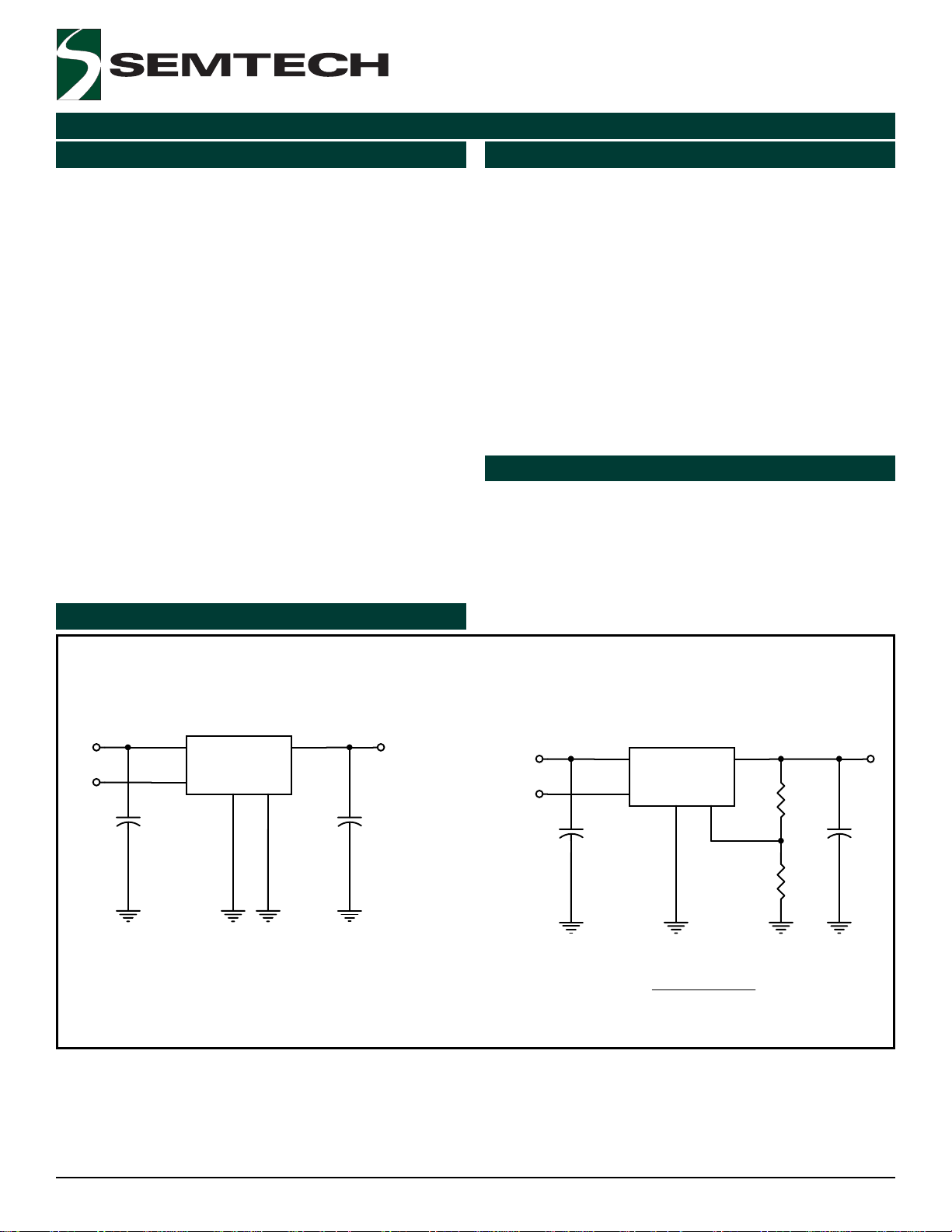
Internally Preset Output Voltage Externally Set Output Voltage
U1 SC1563IS-X.X
VIN VO (X.XV)
C1
1
SHDN
GND
2 3
SHDN
OUTIN
ADJ
45
C2
VIN
SHDN
C1
U1
SC1563IS-X.X
1
SHDN
GND ADJ
2 3
=
V
OUT
R2
45
OUTIN
R1
R2
+
R2)(R11.200
Volts
VO
C2
Revision: January 11, 2006
1 www.semtech.com

SC1563
POWER MANAGEMENT
Absolute Maximum Ratings
Exceeding the specifications below may result in permanent damage to the device, or device malfunction. Operation outside of the parameters
specified in the Electrical Characteristics section is not implied.
retemaraPlobmySmumixaMstinU
egatloVtupnIV
egatloVnwodtuhSV
noitapissiDrewoPP
gnitarepOtneibmAegnaRerutarepmeTT
gnitarepOnoitcnuJegnaRerutarepmeTT
egnaRerutarepmeTegarotST
gnitaRDSEV
Note:
(1) Minimum pad size.
Electrical Characteristics
Unless specified: V
Fixed mode (V
retemaraPlobmySsnoitidnoCniMpyTxaMstinU
= 0V, Adjustable mode (V
SHDN
= GND): VIN = (V
ADJ
+ 0.7V) to 5.5V and I
OUT
NI
NDHS
D
)1(
tneibmAotnoitcnuJecnatsiseRlamrehT
ces01)gniredloS(erutarepmeTdaeLT
ADJ
> V
): V
TH(ADJ)
IN
= 0A to 500mA. Values in bold apply over full operating temperature range.
OUT
θ
AJ
A
J
GTS
DAEL
DSE
= 2.2V to 5.5V and I
= 0A to 500mA,
OUT
4-051ot0C°
7ot3.0-V
Vot3.0-
NI
V
detimiLyllanretnIW
571W/C°
58ot04-C°
051ot56-C°
003C°
2Vk
NI
egnaRegatloVylppuSV
tnerruCtnecseiuQI
NI
Q
V
V
NI
V3.3=58 051 Aµ
NI
V,V5.6=
NDHS
nepO=10.0 00.2 Aµ
2.25.6 V
TUO
)1(
egatloVtuptuO
V
TUO
VNIV=
TUO
I,V7.0+
TUO
Am01=%1-V
TUO
%1+V
)egatloVdexiFlanretnI( %2-%2+
)1(
noitalugeReniL
)1(
noitalugeRdaoL
GER
)ENIL(
GER
)DAOL(
V
V(=
NI
TUO
VNIV=
TUO
I,V5.5ot)V52.0+
TUO
Am01=1.0 4.0 %
V7.0+51.0 04.0 %
2 2006 Semtech Corp. www.semtech.com

POWER MANAGEMENT
Electrical Characteristics
Unless specified: V
Fixed mode (V
retemaraPlobmySsnoitidnoCniMpyTxaMstinU
= 0V, Adjustable mode (V
SHDN
= GND): VIN = (V
ADJ
).tnoC(TUO
)2()1(
egatloVtuoporD
+ 0.7V) to 5.5V and I
OUT
SC1563
> V
ADJ
V
D
): V
TH(ADJ)
= 2.2V to 5.5V and I
IN
= 0A to 500mA. Values in bold apply over full operating temperature range.
OUT
I
TUO
= 0A to 500mA,
OUT
Am2=15Vm
01
I
TUO
Am001=07001Vm
051
I
TUO
Am052=571052Vm
053
I
TUO
Am005=053005Vm
007
timiLtnerruC
I
MIL
5.00.1
A
JDA
)1(
egatloVecnerefeR
V
FER
V
NI
V,V2.2=
V=
JDA
I,
TUO
TUO
Am01=881.1002.1212.1V
671.1422.1
)3(
nerruCniPtsujdAt
)4(
dlohserhTniPtsujdA
I
JDA
V
)JDA(HT
V
V=
JDA
FER
56 051 An
01.0 52.0 04.0 V
NDHS
tnerruCniPnwodtuhSI
dlohserhTniPnwodtuhSV
NDHS
HI
V
NDHS
V,V0=
NI
V
NI
V3.3=5.1 0.5 Aµ
V3.3= 8.1 V
V
LI
V
V3.3= 4.0
NI
noitcetorPerutarepmeTrevO
leveLpirThgiHT
siseretsyHT
IH
TSYH
071°C
01°C
Notes:
(1) Low duty cycle pulse testing with Kelvin connections required.
(2) Defined as the input to output differential at which the output voltage drops to 1% below the value measured at
a differential of 0.7V for 2.5V ≤ V
≤ 3.4V. Not measurable on outputs less than 2.2V due to minimum V
OUT
con-
IN
straints. See typical characteristics curves.
(3) Guaranteed by design.
(4) When V
error amplifier and connects V
exceeds this threshold, the “Sense Select” switch disconnects the internal feedback chain from the
ADJ
instead.
ADJ
3 2006 Semtech Corp. www.semtech.com

POWER MANAGEMENT
Pin Configurations Ordering Information
)3()2()1(
Top View
SOT-23-5
Notes:
(1) Where -X.X denotes voltage options. Available
voltages are: 1.8V, 2.5V, 2.8V, 3.0V, 3.1V and 3.3V.
(2) Output voltage can be adjusted using external
resistors, see Pin Descriptions.
(3) Only available in tape and reel packaging. A reel
contains 3000 devices.
(4) Lead free product. This product is fully WEEE and RoHS
compliant.
rebmuNtraP
RTX.X-KSI3651CS
)4(
TRTX.X-KSI3651CS
Marking Information
SC1563
egakcaP
5-32-TOS
SOT-23-5
63XX = SC1563, voltage option (example: 6318 for 1.8V option)
yyww = Date code (example: 0008 for week 8 of 2000)
4 2006 Semtech Corp. www.semtech.com

POWER MANAGEMENT
Block Diagram
SC1563
Pin Descriptions
#niPemaNniPnoitcnuFniP
1NDHS aottnerructnecseiuqehtgnicuder,fforotalugerehtsnrutneponipsihtgnivaeL.tupnInwodtuhS
2DNG .sesoprupgniknistaehrofdesuebyamnipsihT.dnuorgecnerefeR
3JDA fI.srotsiserkcabdeeflanretniehtybtestahtotegatlovtuptuoehtstes,dednuorgnehw,nipsihT
4TUO.Am005otpugnicruos,ecivedsihtfotuptuorewopehtsinipsihT
5NI V(neewtebebtsumnipsihtottupnieht,daollluftanoitalugerroF.egatlovtupnI
wolebdellupsinipsihtfidelbaneeblliwecivedehT.)An003<yllacipyt(eulavgnitarepostifonoitcarf
.desugniebtonfiDNGottcennoC.V4.0
:)1egapnotiucriCnoitacilppAeeS(eblliwegatlovtuptuoeht,desuerasrotsiserkcabdeeflanretxe
+
=
V
OUT
VmuminiM
NI
.V2.2=
R2
R2)(R11.200
Volts
TUO
.V5.6dna)V7.0+
5 2006 Semtech Corp. www.semtech.com

POWER MANAGEMENT
Introduction
The SC1563 is intended for applications such as
graphics cards where high current capability and very low
dropout voltage are required. It provides a very simple,
low cost solution that uses little pcb real estate.
Additional features include a shutdown pin to allow for a
very low power consumption standby mode, and a fully
adjustable output.
Component Selection
Input capacitor - a 1µF ceramic capacitor is
recommended. This allows for the device being some
distance from any bulk capacitance on the rail.
Additionally, input dr oop due to load transients is reduced,
improving load transient response. Additional capacitance
may be added if required by the application.
SC1563
Output capacitor - a minimum bulk capacitance of 1µF,
along with a 0.1µF ceramic decoupling capacitor is
recommended. Increasing the bulk capacitance will
improve the overall transient response. The use of
multiple lower value ceramic capacitors in parallel to
achieve the desired bulk capacitance will not cause
stability issues. Although designed for use with ceramic
output capacitors, the SC1563 is extremely tolerant of
output capacitor ESR values and thus will also work
comfortably with tantalum output capacitors.
Noise immunity - in very electrically noisy environments,
it is recommended that 0.1µF ceramic capacitors be
placed from IN to GND and OUT to GND as close to the
device pins as possible.
6 2006 Semtech Corp. www.semtech.com

POWER MANAGEMENT
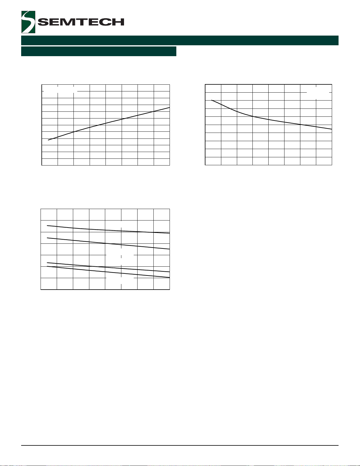
Typical Characteristics
SC1563
Quiescent Current vs. Junction Temperature
vs. Output Current
150
VIN = 3.3V, V
125
100
75
(µA)
Q
I
50
25
0
-50 -25 0 25 50 75 100 125 150
ADJ
= V
I
I
OUT
= 500mA
OUT
= 0mA
OUT
T
(°C)
J
Output Voltage vs. Junction Temperature
vs. Output Current
0.5
VIN = V
0.4
)
0.3
0.2
OUT(NOM)
0.1
0
-0.1
-0.2
Deviation (%V
OUT
-0.3
V
-0.4
-0.5
-50 -25 0 25 50 75 100 125 150
OUT(NOM)
+ 0.7V
I
= 0mA
OUT
= 500mA
I
OUT
T
(°C)
J
Quiescent Current vs. Input Voltage
vs. Output Current
10000
V
= V
ADJ
OUT
1000
I
= 500mA
(µA)
Q
I
100
10
3.0 3.5 4.0 4.5 5.0 5.5 6.0 6.5
OUT
I
= 0mA
OUT
V
(V)
IN
Line Regulation vs. Junction Temperature
vs. Input Voltage Change
0.40
VIN = (V
0.35
I
= 10mA
OUT
0.30
)
0.25
OUT(NOM)
0.20
(%V
LINE
0.15
REG
0.10
0.05
0.00
-50 -25 0 25 50 75 100 125 150
OUT(NOM)
+ 0.25V) to 5.5V
(°C)
T
J
Load Regulation vs.
Junction Temperature
0.20
VIN = V
0.18
0.16
)
0.14
0.12
OUT(NOM)
0.10
(%V
0.08
LOAD
0.06
REG
0.04
0.02
0.00
= 0mA to 500mA
I
OUT
-50 -25 0 25 50 75 100 125 150
OUT(NOM)
+ 0.7V
T
(°C)
J
Dropout Voltage (I
= 0.5A) vs. Output
OUT
Voltage vs. Junction Temperature
700
600
500
400
(mV)
D
300
V
200
100
0
2.2 2.4 2.6 2.8 3.0 3.2 3.4 3.6 3.8 4.0 4.2 4.4 4.6
7 2006 Semtech Corp. www.semtech.com
TJ = 150°C
= 25°C
T
J
T
= -40°C
J
(V)
V
OUT

POWER MANAGEMENT
SC1563
8 2006 Semtech Corp. www.semtech.com
POWER MANAGEMENT
Typical Characteristics (Cont.)
SC1563
Adjust Pin Threshold Voltage
vs. Junction Temperature
400
2.2V ≤ VIN ≤ 6.5V
375
350
325
300
275
(mV)
250
225
TH(ADJ)
V
200
175
150
125
100
-50 -25 0 25 50 75 100 125 150
(°C)
T
J
Shutdown Pin Threshold Voltage vs. Junction
Temperature vs. Input Voltage
1.8
1.6
1.4
VIH, VIN = 6.5V
Shutdown Pin Current vs.
Junction Temperature
2.50
2.25
2.00
1.75
1.50
(µA)
1.25
SHDN
I
1.00
0.75
0.50
0.25
0.00
-50 -25 0 25 50 75 100 125 150
T
(°C)
J
VIN = 3.3V
V
= 0V
SHDN
1.2
(V)
IL
, V
IH
1.0
V
0.8
0.6
0.4
-50 -25 0 25 50 75 100 125 150
T
J
V
V
V
(°C)
, VIN = 6.5V
IL
, VIN = 2.2V
IH
, VIN = 2.2V
IL
9 2006 Semtech Corp. www.semtech.com
POWER MANAGEMENT
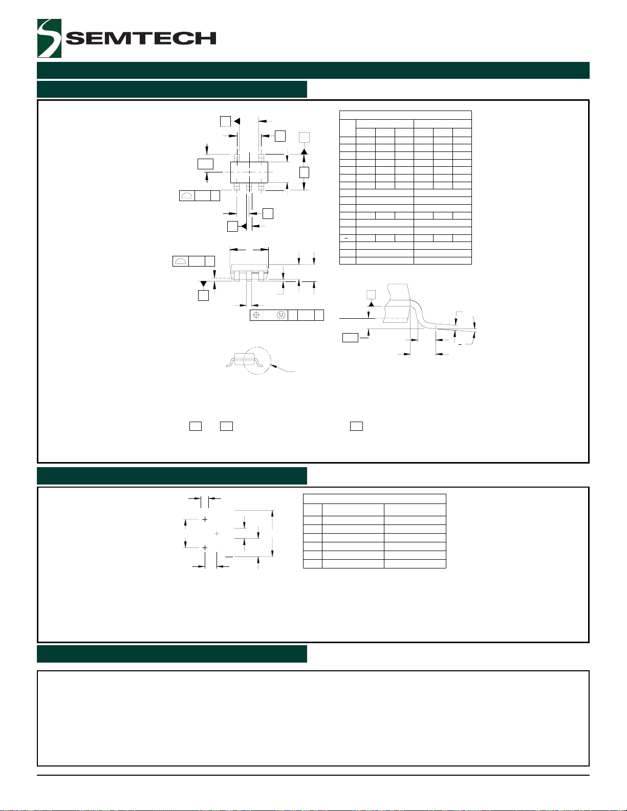
Outline Drawing - SOT-23-5
SC1563
A
e1
D
E/2
N
EI
E
2X
12
ccc
2X N/2 TIPS
e
B
D
aaa C
A2
SEATING PLANE
C
A1
bxN
A
bbb C A-B D
SEE DETAIL
SIDE VIEW
NOTES:
CONTROLLING DIMENSIONS ARE IN MILLIMETERS (ANGLES IN DEGREES).
1.
DATUMS AND TO BE DETERMINED AT DATUM PLANE
2. -A-
DIMENSIONS "E1" AND "D" DO NOT INCLUDE MOLD FLASH, PROTRUSIONS
3.
OR GATE BURRS.
-B- -H-
DIM
GAGE
PLANE
A
A1
A2
E1
e1
L1
01
aaa
bbb
ccc
0.25
A
b
c
D
E
e
L
N
DIMENSIONS
INCHES
MIN NOM
-
.035
-
.000
.035
.045
-
.010
-
.003
.114
.060
.063
.110 BSC
.037 BSC
.012
.018
(.024)
5
-
0°
.004
.008
.008
H
.057
.006 0.00
.051
.020 0.25
.009
.118
.069 1.50
10° 0°
DETAIL
MILLIMETERS
NOMMAX MIN MAX
-
0.90
-
1.15
.90
-
-
0.08
2.80.110
2.90
1.60
2.80 BSC
0.95 BSC
1.90 BSC.075 BSC
0.45.024
0.30
(0.60)
5
-
0.10
0.20
0.20
L
(L1)
A
1.45
0.15
1.30
0.50
0.22
3.00
1.75
0.60
10°
01
c
Land Pattern - SOT-23-5
Contact Information
X
DIM
DIM
C
C
G
(C)
P
NOTES:
1.
THIS LAND PATTERN IS FOR REFERENCE PURPOSES ONLY.
CONSULT YOUR MANUFACTURING GROUP TO ENSURE YOUR
COMPANY'S MANUFACTURING GUIDELINES ARE MET.
G
Z
Y
G
P
P
X
X
Y
Y
Z
Z
DIMENSIONS
DIMENSIONS
INCHES
INCHES
(.098)
.055
.037
.024
.043
.141
Semtech Corporation
Power Management Products Division
200 Flynn Road, Camarillo, CA 930 12
Phone: (805)498-211 1 F AX (805)498-3804
MILLIMETERS
MILLIMETERS
(2.50)
1.40
0.95
0.60
1.10
3.60
10 2006 Semtech Corp. www.semtech.com
 Loading...