


查询SC1175供应商
POWER MANAGEMENT
Description
SC1175
Low Power Dual Synchronous DC/DC
Controller With Current Sharing Circuitry
Features
The SC1175 is a versatile 2 phase, synchronous, voltage mode
PWM controller that may be used in two distinct ways. First, the
SC1175 is ideal for applications where point of use output power
exceeds any single input power budget. Alternatively, the SC1175
can be used as a dual switcher. The SC1175 features a temperature compensated voltage reference, over current protection with
50% fold-back and internal level-shifted, high-side drive circuitry.
In current sharing configuration, the SC1175 can produce a single
output voltage from two separate voltage sources (which can be
different voltage levels) while maintaining current sharing between
the channels. Current sharing is programmable to allow loading
each input supply as required by the application.
In dual switcher configuration, two feedback paths are provided
for independent control of the separate outputs. The device will
provide a regulated output from flexibly configured inputs (3.3V,
5V, 12V), provided 5V is present for VCC. The two switchers are
180° out of phase to minimize input and output ripple.
Applications
u Graphics cards
u DDR Memory
u Peripheral add-in card
u SSTL Termination
u Dual-Phase power supply
u Power supplies requiring two outputs
u 300kHz fixed frequency operation
u Soft Start and Enable function
u Power Good output provided
u Over current protection with 50% fold-back
u Phase-shifted switchers minimize ripple
u High efficiency operation, >90%
u Programmable output(s) as low as 1.25V
u Industrial temperature range
u SOIC 20 pin package
Two Phase, Current Sharing Controller
u Flexible, same or separate V
IN
u Programmable current sharing
u Combined current limit with fold-back
u 2 phases operating opposed for ripple reduction
u Thermal distribution via multi-phase output
Two Independent PWM Controllers
u Flexible, same or separate V
IN
u Independent control for each channel
u Independent and separate current limit
u 2 phases operating opposed for ripple reduction (if same
V
used)
IN
Typical Application Circuit
2 Channels with Current Sharing
Revision 7/31/2000
1
www.semtech.com

POWER MANAGEMENT
Absolute Maximum Rating
retemaraPlobmySstimiLstinU
SC1175
V
CC
DNGot
V
N
I
51ot3.0-V
DNGotDNGP 1±V
DNGotTSB 62ot3.0-V
esaCotnoitcnuJecnatsiseRlamrehT
tneibmAotnoitcnuJecnatsiseRlamrehT
gnitarepO
gnitarepO
egnaRerutarepmeTtneibmA
egnaRerutarepmeTnoitcnuJ
egnaRerutarepmeTegarotST
ces01)gniredloS(erutarepmeTdaeLT
q
CJ
q
AJ
T
A
T
J
GTS
DAEL
03
09
58ot0
521ot0C°
051+ot56-C°
003C°
W/C°
C°
W/
C°
Electrical Characteristics
Unless Specified: VCC = 4.75 to 5.25V, GND = PGND = 0V, FB = VO, 0mV < (CS(+) - CS(-)) < 60mV , TJ = 25°C
RETEMARAPSNOITIDNOCNIMPYTXAMSTINU
egatloVtuptuOI
O
egatloVylppuSV
tnerruCylppuSV
ecnerefeR
noitalugeRdaoLI
noitalugeReniLecnerefeRV5<V
noitalugeReniLtuptuOV5<V
A(niaG
)V
LO
egatloVtimiLtnerruC 060708Vm
)1(
A2=
V,
TUO
CC
0.5=01Am
CC
O
A51otA3.0=
<V515.%
CC
<V515.%
NI
Vot
ESNESO
O
V57.2ottes56.257.258.2V
2.451V
-5732.1
1±
)1(
52.1
1%
-5262.1
1±
53Bd
V
ycneuqerFrotallicsO 072003033zHk
elcyCytuDxaMrotallicsO 0959%
tnerruCkniSHDV5.3=DNGP-HD1A
tnerruCkniSHDV57.1=DNGP-HD5.A
tnerruCecruoSHDV0.5=HD-HTSB1A
tnerruCecruoSHDV5.2=HD-HTSB5.A
2ã 2000 Semtech Corp.
www.semtech.com

SC1175
POWER MANAGEMENT
Electrical Characteristics (Cont.)
Unless Specified: VCC = 4.75 to 5.25V, GND = PGND = 0V, FB = VO, 0mV < (CS(+) - CS(-)) < 60mV , TJ = 25°C
RETEMARAPSNOITIDNOCNIMPYTXAMSTINU
tnerruCkniSLDV5.3=DNGP-LD1A
tnerruCkniSLDV57.1=DNGP-LD5.A
tnerruCecruoSLDV5=LD-LTSB1A
tnerruCecruoSLDV5.2=LD-LTSB5.A
emiTdaeD 05001sn
)2(
tnerruCegrahCtratStfoS
elbanEtratStfoSelcycytud%04.1V
dnEtratStfoSelcycytud%0015.2V
)2(
noitisnarTtratStfoS
)3(
wodniWdooGrewoP
tnerruCkcaBdloFV
eenKegatloVkcaBdloF=II
TUO
MIL
edomsuonorhcnyS3.3V
V0=%05I
52.1V
tnerruCsaiBtupnI2NI-,2NI+,1NI-1Aµ
52Aµ
+01V%
TUO
TUO
MIL
V
NOTES:
(1) Specification refers to application circuit.
(2) The soft start pin sources 25µA to an external capacitor. The converter operates in synchronous mode above the soft
start transition threshold and in asynchronous mode below it.
(3) Power good is an open collector pulled low when the output voltage is outside the ±10% window.
(4) This device is ESD sensitive. Use of standard ESD handling precautions is required.
ã 2000 Semtech Corp.
3
www.semtech.com

POWER MANAGEMENT
SC1175
Pin Configuration
Pin Descriptions
EXPANDED PIN DESCRIPTION
Pin 1: (VREF)
Internal 1.25V reference
Connected to the + input of the master channel error
amplifier.
Pin 2: (+IN)
+ Input of slave channel error amplifier.
Connected to 1.25V reference (Pin 1) for the two
independent channel configuration.
Pin 3, 18: (-IN2, -IN1)
- Inputs of close loop error amplifiers.
Works as a feedback inputs (For both modes).
Pin 4: (VCC)
VCC chip supply voltage.
15V maximum, 10mA typical.
Needs a 1µF ceramic multilayer decoupling capacitor to GND (Pin 20).
Pin 5, 6,15, 16: (CL2-, CL2+, CL1+, CL1-)
Pins (-) and (+) of the current limit amplifiers for both
channels.
Connected to output current sense resistors. Compares that sense voltage to internal 75mV reference.
Needs RC filter for noise rejection.
Pin 7, 14: (BST2, BST1)
BST signal. Supply for high side driver.
Can be connected to a high enough voltage source.
Usually connected to bootstrap circuit.
Pin 8, 13: (DH2, DH1)
DH signal (Drive High).
Gate drive for top MOSFETs.
Requires a small series resistor.
Ordering Information
)1(
ECIVED
RT.WSC5711CS02-OS
1-BVE5711CS
2-BVE5711CS
Notes:
(1) Only available in tape and reel packaging. A reel
contains 1000 devices
EGAKCAP
DRAOB
DRAOB
Marking Information
TOP
yyww = Datecode (Example: 9908)
xxxx = Semtech Lot # (Example: 90101)
Pin 9, 12: (DL2, DL1)
DL signal (Drive Low).
Gate drive for bottom MOSFETs.
Requires a small series resistor.
Pin 10: (PGND)
Power GND. Return of gate drive currents.
Pin 11: (BSTC)
Supply for bottom MOSFETs gate drive.
Pin 17: (SS/ENA)
Soft start pin. Internal current source connected to
external capacitor.
Inhibits the chip if pulled down.
Pin 19: (PWRGD)
Power good signal.
Open collector signal .
Turns to 0 if output voltage is outside the power good
window.
Pin 20: (GND)
Analog GND.
Return of analog signals and bias of chip.
4ã 2000 Semtech Corp.
www.semtech.com
ERAHSTNERRUC
NOITAULAVENOISREV
LENNAHCLAUD
NOITAULAVENOISREV

POWER MANAGEMENT
Block Diagram
SC1175
NOTES
(1) Block 1 (top) is the Master and Block 2 (bottom) is the Slave in current sharing configuration.
(2) For independant operation there is no Master or Slave.
Applications Information
Theory of Operation
Main Loop(s)
The SC1175 is a dual, voltage mode synchronous
Buck controller, the two separate channels are
identical and share only IC supply pins (Vcc and
GND), output driver ground (PGND) and pre-driver
supply voltage (BSTC). They also share a common
oscillator generating a sawtooth waveform for channel 1 and an inverted sawtooth for channel 2. Each
channel has its own current limit comparator. Channel 1 has the positive input of the error amplifier
internally connected to Vref. Channel 2 has both
inputs of the error amplifier uncommitted and available externally. This allows the SC1175 to operate in
two distinct modes.
a) Two independent channels with either com-
mon or different input voltages and different
output voltages. The two channels each have
their own voltage feedback path from their own
ã 2000 Semtech Corp.
5
output. In this mode, the positive input of error
amplifier 2 is connected externally to Vref. If the
application uses a common input voltage, the
sawtooth phase shift between the channels
provides some measure of input ripple current
cancellation.
b) Two channels operating in current sharing
mode with common output voltage and either
common input voltage or different input voltages.
In this mode, channel 1 operates as a voltage
mode Buck controller, as before, but error amp 2
monitors and amplifies the difference in voltage
across the output current sense resistors of
channel 1 and channel 2 (Master and Slave) and
adjusts the Slave duty cycle to match output
currents. Because of finite gain and offsets in the
loop, the resistor ratio for perfect current match-
www.semtech.com

POWER MANAGEMENT
SC1175
Theory of Operation (Cont.)
ing is not 1:1. The Master and Slave channels still
have their own current limits, identical to the
independent channel case.
Power Good
The controller provides a power good signal. This is
an open collector output, which is pulled low if the
output voltage is outside of the power good window.
Soft Start/Enable
The Soft Start/Enable (SS/ENA) pin serves several
functions. If held below the Soft Start Enable threshold, both channels are inhibited. DH1 and DH2 will be
low, turning off the top FETs. Between the Soft Start
Enable threshold and the Soft Start End threshold,
the duty cycle is allowed to increase. At the Soft Start
End threshold, maximum duty cycle is reached. In
practical applications the error amplifier will be
controlling the duty cycle before the Soft Start End
threshold is reached. To avoid boost problems during
startup in current share mode, both channels start
up in asynchronous mode, and the bottom FET body
diode is used for recirculating current during the FET
off time. When the SS/ENA pin reaches the Soft Start
Transition threshold, the channels begin operating in
synchronous mode for improved efficiency. The soft
start pin sources approximately 25uA and soft start
timing can be set by selection of an appropriate soft
start capacitor value.
SENSE RESISTOR SELECTION
Current Sharing Mode
Calculation of the three programming resistors to
achieve sharing.
Three resistors will determine the current sharing
load line.
First the offset resistor will ensure that the load line
crosses the origin (0 Amp on each channel) for
sharing at light current. A pull up resistor from the 5V
bias (VCC of the chip) will be used. For low duty cycle
on the slave channel (below 50%), the pull up will be
on pin 3. For high duty cycle on the slave channel
(above 50%), the pull up will be on pin 2.
The formula is:
OUT
5.X762X100)uppull(R
−Ω=−
V
1.V
+
INSLAVE
100W being the value of the resistors connecting the
pins 2 and 3 to the two output sense resistors.
The estimated voltage drop across the MOSFETs is
0.1V.
Positive values go to pin 3, negative to pin 2.
If R (pull-up) = +20KW then place a 20WK resistor on
pin 3.
If R (pull-up) = -20KW then place a 20KW on pin 2.
Now that the offset resistor has been fixed, we need
to set up the maximum current for each channel.
Selection of R
1 for the master channel:
SENSE
(mohms)
R
Selection of R
R
1 = 72mV / I max master
SENSE
1 = 48mV / I max master
SENSE
2 for the slave channel: (mohms)
SENSE
The errors will be minimized if the power components have been sized proportionately to the maximum currents.
Independent Channels
Calculation of the two current limiting resistors.
There is no need for an offset resistor in the independent channels mode, only the two sense resistors
are used:
Selection of R
R
1 = 72mV / I max ch 1
SENSE
Selection of R
R
1 = 72mV / I max ch 2
SENSE
1 for the channel 1: (mohms)
SENSE
2 for the channel 2: (mohms)
SENSE
6ã 2000 Semtech Corp.
www.semtech.com

POWER MANAGEMENT
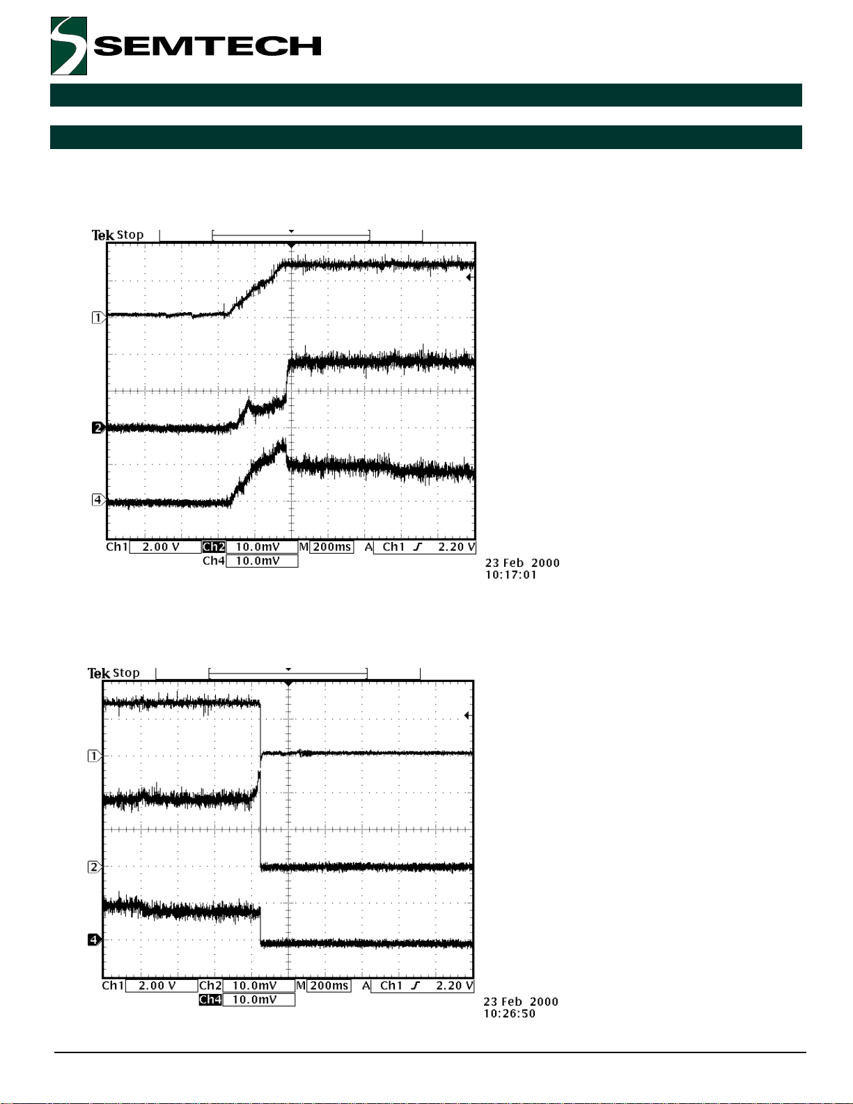
Typical Characteristics - 2 Channels with Current Sharing
SC1175
Figure 1: V
OUT
vs I
PIN Descriptions
IN(5V)
and I
with VCC applied and 4A load. Soft start capacitor = 10nF.
IN(12V)
Ch1: V
Ch2: I
Ch4: I
I
OUT
OUT
(1A/Div)
IN(5V)
(1A/Div)
IN(12V)
: 4.004 Amps
Figure 2: V
OUT
vs I
IN(5V)
and I
with VCC removed and 4A load. Soft start capacitor = 10nF.
IN(12V)
Ch1: V
Ch2: I
Ch4: I
I
OUT
OUT
(1A/Div)
IN(5V)
(1A/Div)
IN(12V)
: 4.004 Amps
ã 2000 Semtech Corp.
7
www.semtech.com
POWER MANAGEMENT
Typical Characteristics - 2 Channels with Current Sharing (Cont.)
SC1175
Figure 3: V
OUT
vs I
IN(5V)
and I
with VCC applied and 12A load. Soft start capacitor = 10nF.
IN(12V)
Ch1: V
Ch2: I
Ch4: I
I
: 12 Amps
OUT
OUT
IN(5V)
IN(12V)
(2A/Div)
(2A/Div)
Figure 4: V
OUT
vs I
IN(5V)
and I
with VCC removed and 12A load. Soft start capacitor = 10nF.
IN(12V)
Ch1: V
Ch2: I
Ch4: I
I
: 12 Amps
OUT
OUT
IN(5V)
IN(12V)
(2A/Div)
(2A/Div)
8ã 2000 Semtech Corp.
www.semtech.com

POWER MANAGEMENT
Typical Characteristics - 2 Channels with Current Sharing (Cont.)
Figure 5: Efficiency data - current sharing mode.
1.0
0.9
0.8
0.7
0.6
0.5
0.4
Efficiency (%)
0.3
0.2
0.1
V
V
V
IN(MASTER)
IN(SLAVE)
= 2.75V
OUT
SC1175
= 12V
= 5V
0.0
0 2 4 6 8 101214
Current (A)
The Current Sharing Evaluation Board is not intended for a specific application. The power components are not
optimized for minimum cost and size. This evaluation board should be used to understand the operation of the
SC1175.
To design with the SC1175 for specific current sharing applications. Please refer to: Application note AN00-3.
ã 2000 Semtech Corp.
9
www.semtech.com
POWER MANAGEMENT
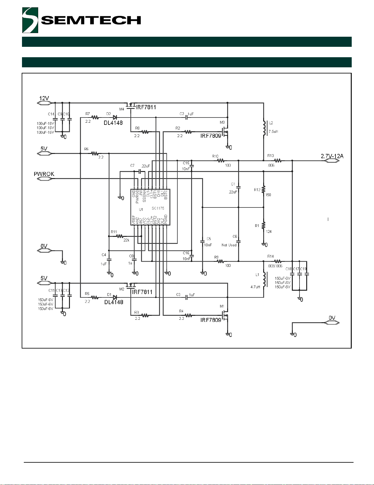
Evaluation Board Schematic - 2 Channel with Current Sharing
SC1175
10ã 2000 Semtech Corp.
www.semtech.com

POWER MANAGEMENT
Evaluation Board Bill of Materials - 2 Channels with Current Sharing
metIytitnauQecnerefeRtraP
127C,1CV05,Fu22.
23 4C,3C,2CV05,Fu1
SC1175
33 61C,51C,5C
418CV05,Fn1
53 41C,01C,9CV6,Fu001
66 91C,81C,71C,31C,21C,11CV61,Fu051
722D,1D8414LD
811LA8,Hu5.7
912LA8,Hu7.4
0123M,1M0307BDFro9087FRI
1124M,2M0307BDFro1187FRI
2111R
317 8R,7R,6R,5R,4R,3R,2R
41201R,9R
51121R
61131R600.
1
0
V05,Fn
421
2.2
001
051
71141R
8111U5711CS
ã 2000 Semtech Corp.
11
300.
www.semtech.com
POWER MANAGEMENT
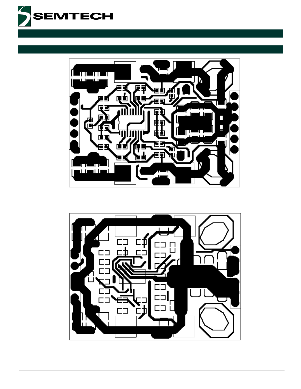
Evaluation Board Gerber Plots - 2 Channels with Current Sharing
SC1175
Top Side Traces
Bottom Side Traces
12ã 2000 Semtech Corp.
www.semtech.com

POWER MANAGEMENT
Typical Characteristics - 2 Independent Channels
Figure 6:
SC1175
Figure 7: Output Current
Input Voltage = 12V @ 5Amps. 2A/DIV.
ã 2000 Semtech Corp.
13
www.semtech.com

POWER MANAGEMENT
Typical Characteristics - 2 Independent Channels (Cont.)
Figure 8: Peak - Peak Output Ripple @ 5A
SC1175
Input Voltage = 12V.
Output Voltage = 2.0V
Figure 9: Phase Node 12V Input @ 5A (without
snubber and RC network.
14ã 2000 Semtech Corp.
www.semtech.com

POWER MANAGEMENT
Typical Characteristics - 2 Independent Channels (Cont.)
Figure 10: Start-up Power On
SC1175
Chan. 1 = Output Current. 2A/DIV.
Chan. 2 = 5V Bias Voltage
Figure 11: Power Off
Chan. 1 = Output Current. 2A/DIV.
Chan. 2 = 5V Bias Voltage
ã 2000 Semtech Corp.
15
www.semtech.com

POWER MANAGEMENT
Typical Characteristics - 2 Independent Channels Efficiency Test
Figure 12:
100
95
90
85
80
EFFICIENCY
75
70
0123456
OUTPUT CURRENT
SC1175
Vin = 12V Vout =
2.0V
Vin = 5V Vout =
1.25V
The Independent Channels Evaluation Board is not intended for a specific application. The power components
are not optimized for minimum cost and size. This evaluation board should be used to understand the operation of the SC1175.
To design with the SC1175 for specific independent channels applications. Please refer to: Application note
AN00-4.
16ã 2000 Semtech Corp.
www.semtech.com

POWER MANAGEMENT
Evaluation Board Schematic - 2 Independent Channels
SC1175
ã 2000 Semtech Corp.
17
www.semtech.com

POWER MANAGEMENT
Evaluation Board Bill of Materials - 2 Independent Channels
metIytitnauQecnerefeRtraP
13 3C,2C,1CV05,Fu1
23 11C,6C,4CV05,Fu22.
315CV05,Fn1
44 01C,9C,8C,7CV05,Fn01
59 02C,91C,81C,71C,61C,51C,41C,31C,21CV6,Fu051
63 32C,22C,12CV61,Fu001
722D,1D8414LD
811LA8,Hu5.7
SC1175
912LA8,Hu7.4
0123M,1M0307BDFro9087FRI
1124M,2M0307BDFro1187FRI
217 7R,6R,5R,4R,3R,2R,1R2.2
313 31R,9R,8R001
41101R600.
51111R022
61121R300.
712 51R,41R421
8111U5711CS
18ã 2000 Semtech Corp.
www.semtech.com
POWER MANAGEMENT
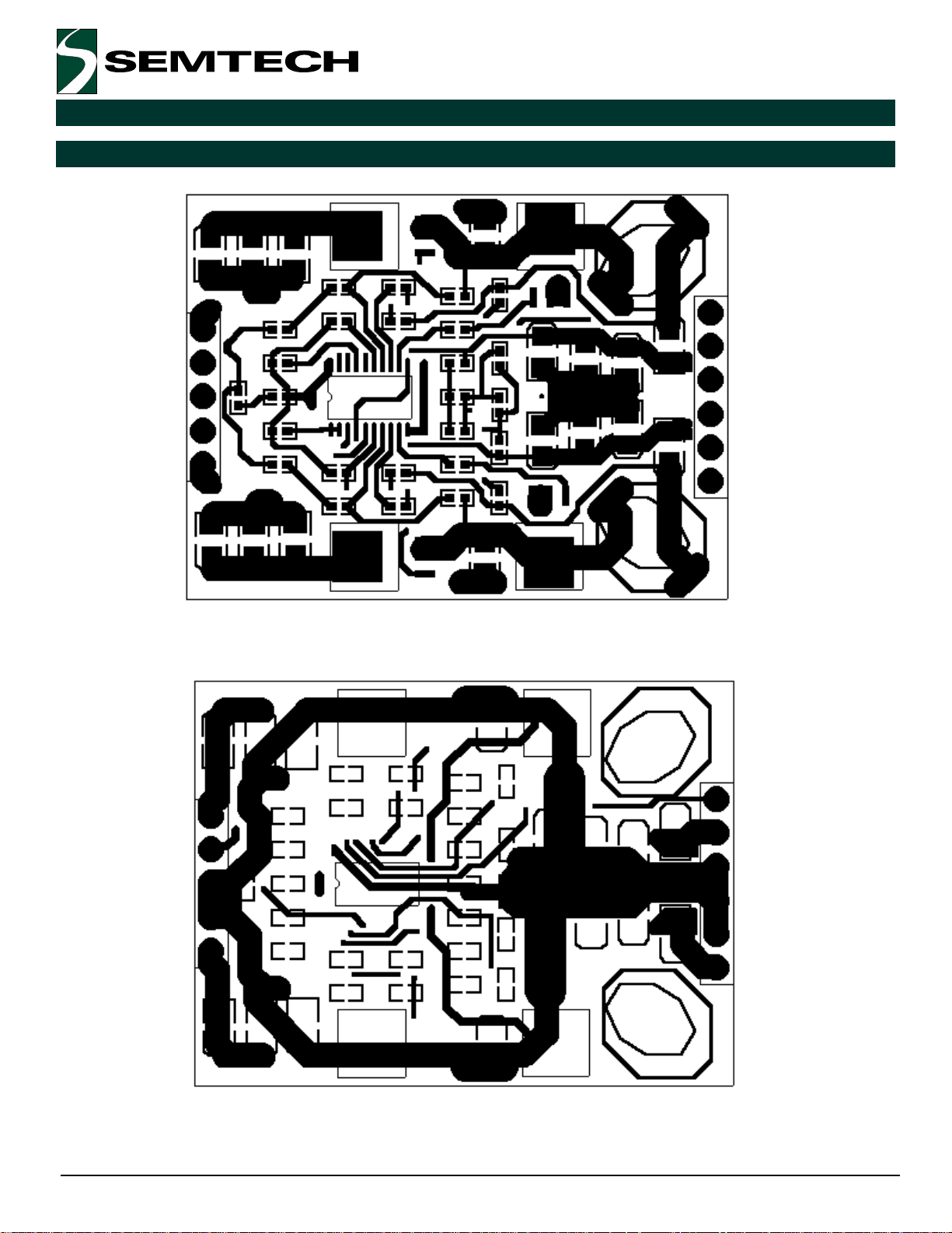
Evaluation Board Gerber Plots - 2 Independent Channels
SC1175
Top Side Traces
ã 2000 Semtech Corp.
Bottom Side Traces
19
www.semtech.com

POWER MANAGEMENT
PCB Layout
SC1175
Power and signal traces must be kept separated for
noise considerations. Feedback, current sense traces
and analog ground should not cross any traces or
planes carrying high switching currents, such as the
input loop or the phase node.
The input loop, consisting of the input capacitors and
both MOSFETs must be kept as small as possible. All
of the high switching currents occur in this loop. The
enclosed loop area must be kept small to minimize
inductance and radiated and conducted emissions.
Designing for minimum trace length is not always the
best approach, often a more optimum layout can be
achieved by keeping loop area constraints in mind.
It is important to keep gate lengths short, the IC must
be close to the power switches. This is more difficult
in a dual channel device than a single and requires
that the two power paths run on either side of a centrally located controller.
Grounding requirements are always conflicting in a
buck converter, especially at high power, and the trick
is to achieve the best compromise. Power ground
(PGND) should be returned to the bottom MOSFET
source to provide the best gate current return path.
Analog ground (GND) should be returned to the
ground side of the output capacitors so that the analog
circuitry in the controller has an electrically quiet
reference and to provide the greatest feedback accuracy. The problem is that the differential voltage
capability of the two IC grounds is limited to about 1V
for proper operation and so the physical separation
between the two grounds must also be minimized. If
the grounds are too far apart, fast current transitions in
the connection can generate voltage spikes exceeding
the 1V capability, resulting in unstable and erratic
behavior.
The feedback divider must be close to the IC and be
returned to analog ground. Current sense traces must
be run parallel and close to each other and to analog
ground.
The IC must have a ceramic decoupling capacitor
across its supply pins, mounted as close to the device
as possible. The small ceramic, noise-filtering capacitors on the current sense lines should also be placed
as close to the IC as possible.
Outline Drawing - SO-20
Contact Information
Contact Information
ECN00-1204
Ref. MS-013AC
Semtech Corporation
Power Management Products Division
652 Mitchell Rd., Newbury Park, CA 91320
Phone: (805)498-2111 FAX (805)498-3804
20ã 2000 Semtech Corp.
www.semtech.com
 Loading...