


查询SC1159EVB供应商
POWER MANAGEMENT
Description
SC1159
Programmable Synchronous DC/DC
Hysteretic Controller with VRM 8.5 VID Range
Features
The SC1159 is a synchronous-buck switch-mode controller designed for use in single ended power supply applications where efficiency is the primary concern. The
controller is a hysteretic type, with a user selectable hysteresis. The SC1159 is ideal for implementing DC/DC
converters needed to power advanced microprocessors
®
such as Pentium
llI and Athlon®, in both single and multiple processor configurations. Inhibit, under-voltage lockout and soft-start functions are included for controlled
power-up.
SC1159 features include an integrated 5 bit D/A converter, temperature compensated voltage reference,
current limit comparator, over-current protection, and an
adaptive deadtime circuit to prevent shoot-through of
the power MOSFET during switching transitions. Power
good signaling, logic compatible shutdown, and over-voltage protection are also provided. The integrated D/A
converter provides programmability of output voltage
from 1.050V to 1.825V in 25mV increments.
The SC1159 high side driver can be configured as either
a ground-referenced or as a floating bootstrap driver.
The high and low side MOSFET drivers have a peak current rating of 2 amps.
Programmable hysteresis
5 bit DAC programmable output (1.050V-1.825V)
On-chip power good and OVP functions
Designed to meet latest Intel specifications
Up to 95% efficiency
+1% tolerance over temperature
Applications
Server Systems and Workstations
Pentium
AMD Athlon
Multiple Microprocessor Supplies
Voltage Regulator Modules
®
III Core Supplies
®
Core Supplies
Typical Application Circuit
R2
1k
R6
20k
+5V
C4
0.01
0.001
+5V
R1
*
R3
*
R4
1k
R5
*
C1
0.1
C2
C3
0.1
R7
*
R8
10k
U1
SC1159CSW
1
IOUT
2
DROOP
3
OCP
4
VHYST
5
VREFB
6
VSENSE
7
AGND
8
SOFTST
9
N/C
10
LODRV
11
LOHIB
12
DRVGND
13
LOWDR
14
DRV
C5
*) for the values see specific application circuit somewhere else in the datasheet
PWRGD
VID25
INHIBIT
IOUTLO
LOSENSE
HISENSE
BOOTLO
HIGHDR
BOOT
VIN12V
28
27
VID0
26
VID1
25
VID2
24
VID3
23
22
21
20
19
18
17
16
15
C10
R10
R9
1k
10k
R11
1k
C8
0.033
Q1
FDB6035AL
R12
1.0
C9
+12V
1.0
Q2
FDB7030BL
R14
1.6
PWRGD
"POWER GOOD"
C6
0.1
INHIB
"INHIBIT"
C7
0.1
L1
0.5uH
Cout
HF
+
Vin +5V/12V
_
+
1.05 to 1.825V
_
Cin
Cin
HF
Bulk
L2
1.0uH
Cout
Bulk
Revision 3, December 2002
1
www.semtech.com

SC1159
POWER MANAGEMENT
Absolute Maximum Ratings
Exceeding the specifications below may result in permanent damage to the device, or device malfunction. Operation outside of the parameters specified
in the Electrical Characteristics section is not implied.
retemaraPlobmySmumixaMstinU
V21NIVNIV
XAM
41ot3.0-V
DNGVRDotTOOB 52ot3.0-V
OLTOOBotTOOB 51ot3.0-V
stupnIlatigiD 3.7ot3.0-V
DNGVRDotDNGA 5.0±V
DNGAotBIHOL 41ot3.0-V
DNGAotESNESOL 41ot3.0-V
DNGAotOLTOI 41ot3.0-V
DNGAotESNESIH 41ot3.0-V
DNGAotESNESV 5ot3.0-V
0
52=
T,noitapissiDrewoPsuounitnoC
A
T,noitapissiDrewoPsuounitnoC
C
erutarepmeTegarotST
CP
0
52=
CP
egnaRerutarepmeTnoitcnuJgnitarepOT
.ceS01)gniredloS(erutarepmeTdaeLT
D
D
J
L
GTS
2.1W
52.6W
521+ot0C°
003C°
051ot56-C°
DC Electrical Characteristics
Unless specified: 0 < TJ < 125°C, VIN = 12V
retemaraPlobmySsnoitidnoCniMpyTxaMstinU
egnaRegatloVylppuSV21NIV4.112131V
)tnecseiuQ(tnerruCylppuSI
ylppuSrevirDediShgiH
)tnecseiuQ(tnerruC
I
qgniruddlohserhtOLVUevobaniV,V5=HNI
NI
qdlohserhtOLVUwolebniVroVO=HNI
TOOB
51Am
,pu-trats
f
ws
C
C=
HD
LD
Fp05=
,V0=OLTOOB,zHk002=
01Aµ
,pu-tratsgnirud
V0=OLTOOB,V31=TOOB
dlohserhtOLVUevobaNIV,V5=HNI
5Am
,pu-tratsgnirud
f
ws
C
HD
Fp05=
2 2002 Semtech Corp.
,V0=OLTOOB,V31=TOOB,zHk002=
www.semtech.com

POWER MANAGEMENT
DC Electrical Characteristics
(Cont.)
Unless specified: 0 < TJ < 125°C, VIN = 12V
retemaraPslobmySsnoitidnoCniMpyTxaMstinU
noitacifitnedIegatloV/ecnerefeR
SC1159
ycaruccAegatloVecnerefeRV
FER
)elbaT
dlohserhThgiHVm52DIV-0DIV
V
)H(HT
egatloV
dlohserhTwoLVm52DIV-0DIV
V
)L(HT
egatloV
dooGrewoP
dlohserhTegatlovrednUV
egatloVnoitarutaStuptuOV
siseretsyHV
)DGRWP(HT
I
TAS
O
)DGRWP(SYH
Am5=5.0V
noitcetorPegatloVrevO
tnioPpirTPVOV
)1(
siseretsyH
PVO
V
)PVO(SYH
tratStfoS
tnerruCegrahCI
V
GHC
SS
k02=DNGAotnip ,Ω V
I(=
I:etoN
GHC
tnerruCegrahcsiDghcsidIV
V1=1Am
)SS(
BFERV
llufrevo,V6.21<V21NIV<V4.11
1-1%
egatloVtuptuOees(egnarDIV
52.2V
1V
2888V%
FER
01Vm
215102V%
TUO
01Vm
BFERVmorfecnatsiser,V5.0=
V3.1=
BFER
4.01316.51Aµ
)5/
dlohserhTtratStratsV
OLVUV21NIV
dlohserhTtratStratsV
siseretsyHsyhV
tnerruCsaiBtupnIsaibI
gnitteSsiseretsyHV
2002 Semtech Corp.
rotarapmoCtibihnI
)HN(
OLVU
OLVU
rotarapmoCciteretsyH
egatloVtesffOtupnIsoV
ycaruccAsiseretsyHV
V
PMCSYH
PMCSYH
CCASYH
TESSYH
POORD
3
dednuorgnip5Vm
10.24.2V
52.952.0152.11V
8.122.2V
1Au
7Vm
06Vm
www.semtech.com

POWER MANAGEMENT
DC Electrical Characteristics (Cont.)
retemaraPslobmySsnoitidnoCniMpyTxaMstinU
noitasnepmoCpoorD
SC1159
ycaruccAlaitinIV
V
CCAPOORD
POORD
Vm05=5Vm
noitcetorPtnerrucrevO
tnioPpirTPCOV
tnerruCsaiBtupnIsaibI
PCO
PCO
90.01.011.0V
001An
gnisneSSDVediS-hgiH
niaG 2V/V
ycaruccAlaitinIV
ecruoSTUOIecruosI
tnerruCkniSTUOI
knisI
V
gniwSegatloVTUOIVV
V
egatloVtupnIleveLhgiHESNESOLhiV
egatloVtupnIleveLwoLESNESOLliV
V
CCATUOI
TUOI
TUOI
)11(TUOI
)V5.4(TUOI
)V3(TUOI
ESNESOL
ESNESOL
ESNESIH
V
TUOI
V
OLTUOI
V
TUOI
V
OLTUOI
V
ESNESIH
V
ESNESIH
V
ESNESIH
V
ESNESIH
V
ESNESIH
V,V21=
OLTUOI
V,V5.0=
ESNESIH
V5.11=
V,V50.0=
ESNESIH
V21=
R,V11=
TUOI
R,V5.4=
TUOI
R,V3=
TUOI
V9.11=6Vm
,V21=
,V21=
005Aµ
0405Aµ
K01= Ω 057.3V
k01= Ω 00.2V
k01= Ω 00.1V
)1etoN(V5.4=58.2V
)1etoN(V5.4=8.1V
ecnatsiseRdloH/elpmaSR
H/S
)1etoN(055608
ecnerefeRdereffuB
noitalugeRdaoLBFERVgerdlV
BFER
I<Aµ01
BFER
Aµ005<2Vm
)1(tiucriCemitdaeD
egatloVleveLhgiHBIHOLhiV
egatloVtupnIleveLwoLBIHOLliV
egatloVtupnIleveLhgiHRDWOLhiV
egatloVtupnIleveLwoLRDWOLliV
BIHOL
BIHOL
RDWOL
RDWOL
rotalugeRevirD
egatloVVRDV
noitalugeRdaoLgerdlV
tnerruCtiucriCtrohStrohsI
VRD
VRD
VRD
I<Am1
VRD
4 2002 Semtech Corp.
I,V6.21<V21NIV<4.11
VRD
Am05<001Vm
Ω
2V
0.1V
2V
0.1V
Am05=7 9V
001Am
www.semtech.com

POWER MANAGEMENT
DC Electrical Characteristics (Cont.)
retemaraPlobmySsnoitidnoCniMpyTxaMstinU
revirDtuptuOediS-hgiH
SC1159
tnerruCtuptuOkaePcrsI
tuptuOtnelaviuqE
ecnatsiseR
RDHGIH
T
J
knisI
crsR
V
RDHGIH
T
RDHGIH
J
V
knisR
T
RDHGIH
J
V
revirDtuptuOediS-woL
tnerruCtuptuOkaePcrsI
RDWOL
T
knisI
J
V
RDWOL
V
tuptuOtnelaviuqE
crsR
ecnatsiseR
knisR
T
RDWOL
J
V
T
RDWOL
J
V
AC Electrical Characteristics (Note 1)
,su001<wpt,%2<elcycytud
C°521=
V-
TOOB
Vro
OLTOOB
RDHGIH
V,V5.6=
RDHGIH
,)crs(V5.1=
)knis(V5=
C°521=
V-
TOOB
OLTOOB
V,V5.6=
V6=
RDHGIH
C°521=
V-
TOOB
OLTOOB
V,V5.6=
V5.0=
RDHGIH
,su001<wpt,%2<elcycytud
C°521=
VRD
RDWOL
V,V5.6=
RDWOL
)knis(V5=
ro,)crs(V5.1=
C°521=
VRD
V,V5.6=
V6=
RDWOL
C°521=
VRD
V,V5.6=
RDWOL
V5.0=
2
A
54
Ω
5
2
A
54
Ω
5
retemaraPlobmySsnoitidnoCniMpyTxaMstinU
srotarapmoCciteretsyH
emiTyaleDnoitagaporP
t
roRDHGIHotESNESVmorf
PORPCH
V3.1 ≤ ferV ≤ V8.1
,evirdrevoVm01
051052sn
gnidulcxe(RDWOL
)emitdaed
srevirDtuptuO
emitllaf/esirRDHGIHrt
emitllaf/esirRDWOLrt
RDHGIH
rt
ft
T
RDHGIH
J
RDWOL
T
RDWOL
J
V,Fn9=IC
TOOB
C°521=
V,Fn9=IC
VRD
C°521=
V,v5.6=
OLTOOB
,dednuorg=
,V5.6=
06sn
06sn
noitcetorPtnerrucrevO
noitagaporProtarapmoC
t
PORPVO
1sµ
emiTyaleD
sedulcnI(emiThctilgeD
t
LGDVO
25sµ
noitagaporprotarapmoc
)emityaled
2002 Semtech Corp.
5
www.semtech.com

POWER MANAGEMENT
AC Electrical Characteristics (Cont.) (Note 1)
retemaraPslobmySsnoitidnoCniMpyTxaMstinU
noitcetorPegatlovrevO
SC1159
emiTyaleDnoitagaporProtarapmoCt
rotarapmocsedulcnI(emiThctilgeD
)emityalednoitcetorp
PORPVO
t
LGDVO
13sµ
1sµ
gnisneSsdVediS-hgiH
emiTesnopseRt
V
PSERSDV
ESNESIH
V,V21=
OLTUOI
deslup
esirsn001,V9.11otV21morf
2sµ
semitllafdna
V
ESNESIH
V,V5.4=
OLTUOI
deslup
esirsn001,V4.4otV5.4morf
3sµ
semitllafdna
V
ESNESIH
V,V3=
OLTUOI
deslup
esirsn001,V9.2otV0.3morf
3sµ
semitllafdna
egdEgnisiRnoitcetorPtiucriCtrohS
yaleD
ffo-nrut/no-nruthctiwSdloH/elpmaS
yaleD
t
DERSDV
V<V3
t
YLDXWS
V
ESNESIH
V=
ESNESOL
dednuorgESNESOL003005sn
V11<
ESNESIH
03001sn
dooGrewoP
yaleDnoitagaporProtarapmoCt
DGRWP
tratstfoS
yaleDnoitagaporProtarapmoCt
TSLS
Vm01=evirdrevo065009sn
emitdaeD
C
emiTpalrevo-noNrevirDt
LON
RDWOL
RDWOL
nodlohserht%01,Fn9=
03001sn
VRDOL
yaleDnoitagaporPT
YLDVRDOL
Note:
(1) Guaranteed, but not tested.
(2) This device is ESD sensitive. Use of standard ESD handling precautions is required.
1sµ
004sn
6 2002 Semtech Corp.
www.semtech.com
POWER MANAGEMENT
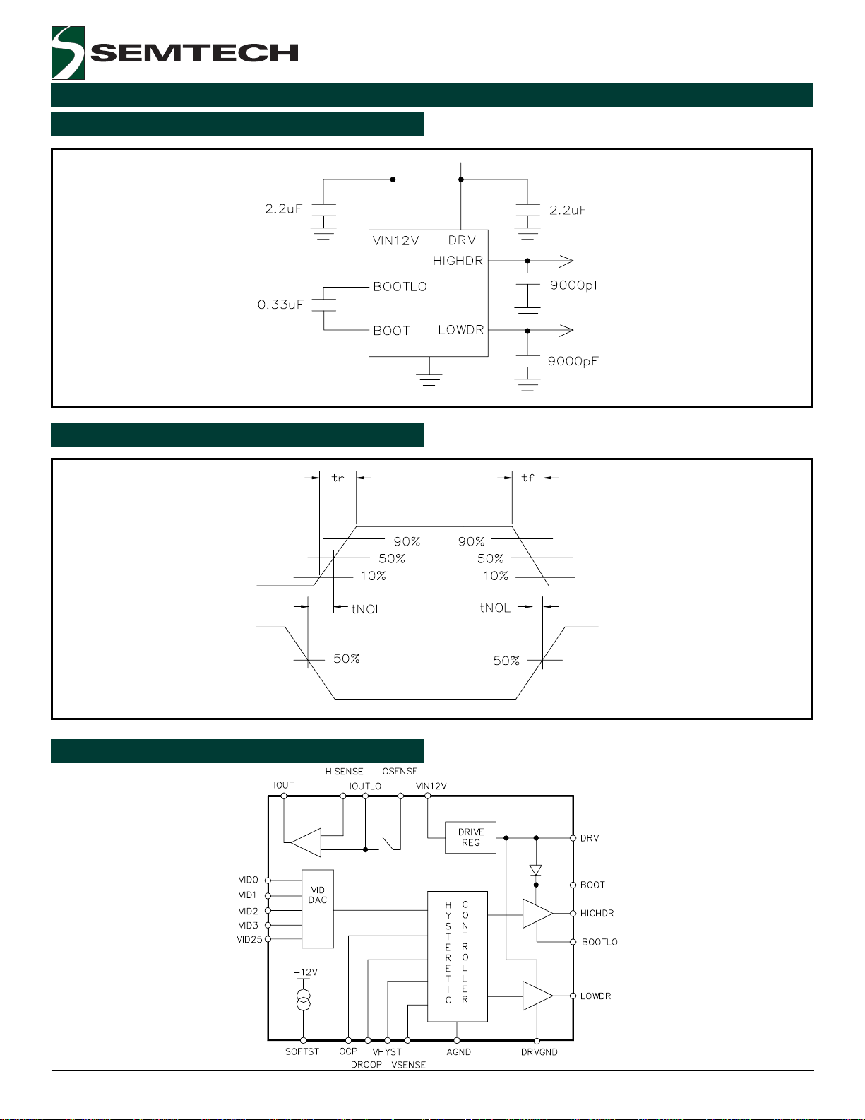
Test Circuit
Timing Diagram
SC1159
Simplified Block Diagram
2002 Semtech Corp.
7
www.semtech.com

POWER MANAGEMENT
SC1159
Pin Configuration
Top View
(28-Pin SOIC)
Ordering Information
)1(
eciveD
RTWS9511CS82-OSC°521ot°0
BVE9511CSdraoBnoitaulavE
Note:
(1) Only available in tape and reel packaging. A reel
contains 1000 devices.
egakcaPT(egnaRpmeT
)
J
Pin Descriptions
#niPemaNniPnoitcnuFniP
1TUOI derusaemsatnerrucdaolehtotlanoitroporpsinipsihtnoegatlovtuptuoehT.tuOtnerruC
POORD asapoordtniop-tesegatlovtuptuofotnuomaehttesotdesusinipsihT.egatloVpoorD
2
3PCO aybnoitcetorptnerrucrevoroftnioppirtehttesotdesusinipsihT.noitcetorPtnerruCrevO
4TSYHV rotsiseraybderiuqersiseretsyhfotnuomaehttesotdesusinipsihT.niPteSsiseretsyH
5BFERV.)yrtiucricDIVmorf(egatloVecnerefeRdereffuB
6ESNESV.esneSegatloVtuptuO
7DNGA.dnuorGlatigiDdnagolanAlangiSllamS
8TSTFOS .yaledemitehtstesDNGAotnipsihtmorfroticapacagnitcennoC.tratStfoS
9CN.detcennoctoN
01VRDOL siBIHOLnehW.noitarepolamronselbaneV5+otnipsihtgnitcennoC.lortnoCevirDwoL
I
DRx2otlauqeyletamixorppasidna,TEFSOMedishgihehtssorca
x)NO(S
.DAOL
.DNGAdnaTUOIneewtebredividrotsiseraybtessiegatlovehT.tnerrucdaolfonoitcnuf
.DNGAdnaTUOIneewtebredividrotsiser
.DNGAdnaBFERVneewtebredivid
.RDWOLlortnocotdesuebnacnipsiht,dednuorg
11BIHOL .tnerrucurht-toohsetanimileotdesusinipsihT.tibihnIediSwoL
21DNGVRD .nipsihtotdetcennocsidnuorgroticapactuptuoerusnI.dnuorGrewoP
31RDWOL .TEFSOMediswolfoetagottcennoC.tuptuOrevirDediSwoL
8 2002 Semtech Corp.
www.semtech.com

POWER MANAGEMENT
Pin Descriptions (Cont.)
#niPemaNniPnoitcnuFniP
41VRD.srevirDTEFSOMehtrofrotalugeRevirD
51V21NIV.liarrewopV21ottcennoC.ylppuSV21
61TOOB .revirdTEFedishgihehtrofevirdgnitaolfaetarenegotdesusinipsihT.partstooB
71RDHGIH .TEFSOMedishgihfoetagottcennoC.tuptuOrevirDediShgiH
81OLTOOB .DNGVRDottcennocnipsiht,snoitacilppapotksednI.woLpartstooB
91ESNESIH afoedistupniehtro,TEFedishgihehtfoniardehtotdetcennoC.esneStnerruChgiH
02ESNESOL afoedisTEFehtro,TEFedishgihehtfoecruosehtotdetcennoC.esneStnerruCwoL
12OLTUOI ehtnoegatlovsinipsihtnoegatloV.gelmottobsroticapacgnilpmasehtsisihT
SC1159
.TEFedishgihehtdnatupniehtneewtebrotsiseresnestnerruc
.TEFedishgihehtdnatupniehtneewtebrotsiseresnestnerruc
.nosiTEFedishgihehtnehwnipESNESOL
22TIBIHNI otdetcennocyllausU.delbasiderasrevirdTEFSOMeht,dednuorgsinipsihtfI.tibihnI
3252DIV.tupnIgnimmargorP
423DIV.tupnIgnimmargorP
522DIV.tupnIgnimmargorP
621DIV.tupnIgnimmargorP
720DIV.tupnIgnimmargorP
82DGRWP nihtiwsiegatlovtuptuoehtfihgihsituptuocigolrotcellocneposihT.dooGrewoP
.rotsiserpu-llupahguorhtV5+
.tnioptesehtfo%51
2002 Semtech Corp.
9
www.semtech.com

POWER MANAGEMENT
Block Diagram
VIN12V
Vcc
DRIVE
REGULATOR
DRV
BOOT
HIGHDR
BOOTLO
LOWDR
SC1159
DRVGND
SOFTST
LOSENSE
IOUTLOHISENSEIOUT
+
+
-
-
PREREG
ANALOG BIAS
G=2
I(VREFB) / 5
DELAY
RISING EDGE
+
HIGHDR
-
LOWDR
FILTER
1.15VREF 0.85VREF
SHUTDOWN
+
+-
--+
VID
FILTER
+
DAC
+
VREF
--+
-
FILTER
VREF
-
LODRV
+
VREFB
VHYST
VSENSE LOHIB
DROOP
VID25
VID3
VID2
VID1
VID0
PWRGD
50uA
FAULT
Q
R
BANDGAP
S
+
-
UVLO
0.85VREF
INH
DEGLITCH
10 2002 Semtech Corp.
DEGLITCH
+
-
+
-
Vcc
2V
10V
+
-
+
-
VSENSE
INHIBIT
AGND
OCP
100mV
1.15VREF
www.semtech.com

POWER MANAGEMENT
Output Voltage Table
0 = GND, 1 = OPEN
)2(
Vm52DIV
00100 50.1
10 10 0 570.1
00011 01.1
100 11 521.1
00010 51.1
100 10 571.1
00001 02.1
10001 522.1
00000 52.1
10000 572.1
01111 03.1
SC1159
)1(
3DIV
)1(
2DIV
)1(
1DIV
)1(
ODIV
)V(CDV
11111 523.1
01110 53.1
11110 573.1
01101 04.1
11101 524.1
01100 54.1
11100 574.1
01011 05.1
11011 525.1
01010 55.1
11010 575.1
01001 06.1
11001 526.1
01000 56.1
11000 576.1
00111 07.1
10111 527.1
00110 57.1
10 1 10 577.1
0010 1 08.1
10 10 1 528.1
NOTE:
(1) VID (3:0) correspond to legacy VRM 8.4 voltage levels for 1.3V - 1.8V.
(2) VID 25mV provides a 25mV increment.
2002 Semtech Corp.
11
www.semtech.com

POWER MANAGEMENT
Applications Information - Functional Description
SC1159
Reference/Voltage Identification
The reference/voltage identification (VID) section consists of a temperature compensated bandgap reference
and a 5-bit voltage selection network. The 5 VID pins
are TTL compatable inputs to the VID selection network.
They are internally pulled up to +3.3V generated from
the +12V supply by a resistor divider, and provide programmability of output voltage from 1.050V to 1.825V
in 25mV increments.
Refer to the Output Voltage Table for the VID code settings. The output voltage of the VID network, VREF is
within 1% of the nominal setting over the full input and
output voltage range and junction temperature range.
The output of the reference/VID network is indirectly
brought out through a buffer to the REFB pin. The voltage on this pin will be within 3mV of VREF. It is not recommended to drive loads with REFB other than setting
the hysteresis of the hysteretic comparator, because the
current drawn from REFB sets the charging current for
the soft start capacitor. Refer to the soft start section
for additional information.
Hysteretic Comparator
The hysteretic comparator regulates the output voltage
of the synchronous-buck converter. The hysteresis is
set by connecting the center point of a resistor divider
from REFB to AGND to the HYST pin. The hysteresis is
set by connecting the center point of a resistor divider
from REFB to AGND to the HYST pin. The hysteresis of
tne comparator will be equal to twice the voltage difference between REFB and HYST, and has a maximum value
of 60mV. The maximum propagation delay from the comparator inputs to the driver outputs is 250ns.
Low Side Driver
The low side driver is designed to drive a low R
channel MOSFET, and is rated for 2 amps source and
sink. The bias for the low side driver is provided internally from VDRV.
DS(ON)
N-
configured as a floating driver, the bias voltage to the
driver is developed from the DRV regulator. The internal
bootstrap diode, connected between the DRV and BOOT
pins, is a Schottky for improved drive efficiency. The
maximum voltage that can be applied between the BOOT
pin and ground is 25V. The driver can be referenced to
ground by connecting BOOTLO to PGND, and connecting
+12V to the BOOT pin.
Deadtime Control
Deadtime control prevents shoot-through current from
flowing through the main power FETs during switching
transitions by actively controlling the turn-on times of the
FET drivers. The high side driver is not allowed to turn on
until the gate drive voltage to the low-side FET is below 2
volts, and the low side driver is not allowed to turn on
until the voltage at the junction of the 2 FETs (VPHASE) is
below 2 volts. An internal low-pass filter with an 11MHz
pole is located between the output of the low-side driver
(DL) and the input of the deadtime circuit that controls
the high-side driver, to filter out noise that could appear
on DL when the high-side driver turns on.
Current Sensing
Current sensing is achieved by sampling and holding the
voltage across the high side FET while it is turned on.
The sampling network consists of an internal 50Ω switch
and an external 0.1µF hold capacitor. Internal logic controls the turn-on and turn-off of the sample/hold switch
such that the switch does not turn on until VPHASE transitions high and turns off when the input to the high side
driver goes low. Thus sampling will occur only when the
high side FET is conducting current. The voltage at the
IO pin equals 2 times the sensed voltage. In applications where a higher accuracy in current sensing is required, a sense resistor can be placed in series with the
high side FET and the voltage across the sense resistor
can be sampled by the current sensing circuit.
Droop Compensation
High Side Driver
The high side driver is designed to drive a low R
channel MOSFET, and is rated for 2 amps source and
sink current. It can be configured either as a ground
referenced driver or as a floating bootstrap driver. When
DS(ON)
N-
The droop compensation network reduces the load transient overshoot/undershoot at VOUT, relative to VREF.
VOUT is programmed to a voltage greater than VREF equal
to VREF • (1+R7/R8) (see Typ. App. Circuit, Pg 1) by an
external resistor divider from VOUT to the VSENSE pin to
reduce the undershoot on VOUT during a low to high load
12 2002 Semtech Corp.
www.semtech.com

POWER MANAGEMENT
Applications Information - Functional Description (Cont.)
SC1159
current transient. The overshoot during a high to low
load current transient is reduced by subtracting the voltage that is on the DROOP pin from VREF. The voltage on
the IO pin is divided down with an external resistor divider, and connected to the DROOP pin. Thus, under
loaded conditions, VOUT is regulated to:
VOUT = VREF • (1+R7/R8) - IOUT • R2/(R1+R2).
Inhibit
The inhibit pin is a TTL compatible digital pin that is used
to enable the controller. When INH is low, the output
drivers are low, the soft start capacitor is discharged,
the soft start current source is disabled, and the controller is in a low IQ state. When INH goes high, the short
across the soft start capacitor is removed, the soft start
current source is enabled, and normal converter operation begins. When the system logic supply is connected
to INH, it controls power sequencing by locking out controller operation until the system logic supply exceeds
the input threshold voltage of the INH circuit; thus the
+12V supply and the system logic supply (either +5V or
3.3V) must be above UVLO thresholds before the controller is allowed to start up.
VIN
proportional to VREF, the power-up time for VOUT will be
independent of VREF. Thus, C
can remain the same
SS
value for all VID settings. The soft start charging current
is determined by the following equation: I
Where I
is the current flowing out of the REFB pin. It
REFB
SS
= I
REFB
/5.
is recommended that no additional loads be connected
to REFB, other than the resistor divider for setting the
hysteresis voltage. Thus these resistor values will determine the soft start charging current. The maximum current that can be sourced by REFB is 500µA.
Power Good
The power good circuit monitors for an undervoltage condition on VOUT. If VSENSE is 15% (nominal) below VREF,
then the power good pin is pulled low. The PWRGD pin is
an open drain output.
Overvoltage Protection
The overvoltage protection circuit monitors VOUT for an
overvoltage condition. If VSENSE is 15% above VREF,
than a fault latch is set and both output drivers are turned
off. The latch will remain set until VIN goes below the
undervoltage lockout value. A 1ms deglitch timer is included for noise immunity.
The VIN undervoltage lockout circuit disables the controller while the +12V supply is below the 10V start
threshold during power-up. While the controller is disabled, the output drivers will be low, the soft start capacitor will be shorted and the soft start current is disabled and the controller will be in a low IQ state. When
VIN exceeds the start threshold, the short across the
soft start capacitor is removed, the soft start current
source is enabled and normal converter operation begins. There is a 2V hysteresis in the undervoltage lockout circuit for noise immunity.
Soft Start
The soft start circuit controls the rate at which VOUT powers up. A capacitor is connected between SS and AGND
and is charged by an internal current source. The value
of the current source is proportional to the reference
voltage so the charging rate of CSS is also proportional to
the reference voltage. By making the charging current
Overcurrent Protection
The overcurrent protection circuit monitors the current
through the high side FET. The overcurrent threshold is
adjustable with an external resistor divider between IO
and AGND, with the divider voltage connected to the OCP
pin. If the voltage on the OCP pin exceeds 100mV, then
a fault latch is set and the output drivers are turned off.
The latch will remain set until VIN goes below the
undervoltage lockout value. A 1ms deglitch timer is included for noise immunity. The OCP circuit is also designed to protect the high side FET against a short-toground fault on the terminal common to both power FETs
(VPHASE).
Drive Regulator
The drive regulator provides drive voltage to the low side
driver, and to the high side driver when the high side
driver is configured as a floating driver. The minimum
drive voltage is 7V. The minimum short circuit current is
100mA.
2002 Semtech Corp.
13
www.semtech.com

POWER MANAGEMENT
Application Circuit
SC1159
+5V
R11
R10
1k
10k
+12V
+12V
"POWER GOOD"
PWRGD
C9
0.1
28
Vout
C47-58
10.0
1500uF 6.3V
D2(opt)
MBRB2515L
2pl.
C35,36
0.0022
1.6
_
GND/OUT
2pl.
GND
INHIB
"INHIBIT"
C10
R12
+
POS/OUT
+
POS/IN
L1
0.5uH
0.1
1k
_
Vin +5V/12V
C24-32
820uF 16V
1.0
C15-23
0
R14,15,16
R13
0
GND/IN
R17
NS
R19
C12
R18
0
22.0
C37-46
L2
1.0uH@40A
3.3
R26,27
2pl.
2pl.
C33,34
0.0022
R24,25
3.3
NS
Q2
FDB6035AL
R21
1.0
Q4
FDB7030BL
R23
40A+ Evaluation Board
Q1
D1
FDB6035AL
19
MBRA130L
18
R20
1.0
17
C11
0.033
J0
J1
J2
J3
J4
24
25
26
27
22
21
23
20
Q3
FDB7030BL
R22
1.6
C13
1.0
+12V
15
16
C14
2.2
VID0
PWRGD
U1
SC1159
IOUT1DROOP2OCP3VHYST4VREFB5VSENSE6AGND7SOFTST8N/C9LODRV10LOHIB11DRVGND12LOWDR13DRV
R5
R3
4.3k
R1
2k
R4
1k
C2
0.001
C1
0.001
R2
1k
VID25
INHIBIT
IOUTLO
C4
0.1
C3
0.1
100
R6
C5
0.001
20k
LOSENSE
C6
0.1
+5V
R7
HISENSE
100
C7
0.01
BOOTLO
HIGHDR
VID3
VID2
VID1
14 2002 Semtech Corp.
BOOT
VIN12V
14
C59
1.0
C8
2.2
R9
150
R8
10k
www.semtech.com

POWER MANAGEMENT
Typical Characteristics
V V
= 5V; I = 5V; I
V
= 5V; I
V V
= 5V; I = 5V; I
ININ
IN
ININ
“Droop” & “Offset” Disabled“Droop” & “Offset” Disabled
“Droop” & “Offset” Disabled
“Droop” & “Offset” Disabled“Droop” & “Offset” Disabled
VV
V
VV
= 0A to 40A = 0A to 40A
= 0A to 40A
= 0A to 40A = 0A to 40A
OUTOUT
OUT
OUTOUT
= 1.8V = 1.8V
= 1.8V
= 1.8V = 1.8V
OUTOUT
OUT
OUTOUT
SC1159
100%
90%
80%
70%
60%
50%
40%
Efficiency
30%
20%
10%
0%
0 5 10 15 20 25 30 35 40
Current, A
100%
90%
80%
70%
60%
50%
40%
Efficiency
30%
20%
10%
0%
0 5 10 15 20 25 30 35 40
Current, A
VV
V
VV
OUTOUT
OUT
OUTOUT
Regulation
= 1.5V = 1.5V
= 1.5V
= 1.5V = 1.5V
Regulation
3%
2%
1%
0%
-1%
-2%
-3%
0 5 10 15 20 25 30 35 40
Current, A
3%
2%
1%
0%
-1%
-2%
-3%
0 5 10 15 20 25 30 35 40
Current, A
100%
90%
80%
70%
60%
50%
40%
Efficiency
30%
20%
10%
0%
0 5 10 15 20 25 30 35 40
2002 Semtech Corp.
Current, A
= 1 = 1
..
= 1
= 1 = 1
15
1V1V
.
1V
..
1V1V
3%
2%
1%
0%
-1%
Regulation
-2%
-3%
0 5 10 15 20 25 30 35 40
Current, A
www.semtech.com
VV
V
VV
OUTOUT
OUT
OUTOUT

POWER MANAGEMENT
Typical Characteristics (Cont.)
V V
= 12V; I = 12V; I
V
= 12V; I
V V
= 12V; I = 12V; I
ININ
IN
ININ
“Droop” & “Offset” Disabled“Droop” & “Offset” Disabled
“Droop” & “Offset” Disabled
“Droop” & “Offset” Disabled“Droop” & “Offset” Disabled
VV
V
VV
OUTOUT
OUT
OUTOUT
= 0A to 40A = 0A to 40A
= 0A to 40A
= 0A to 40A = 0A to 40A
OUTOUT
OUT
OUTOUT
= 1.8V = 1.8V
= 1.8V
= 1.8V = 1.8V
SC1159
100%
90%
80%
70%
60%
50%
40%
Efficiency
30%
20%
10%
0%
0 5 10 15 20 25 30 35 40
Current, A
100%
90%
80%
70%
60%
50%
40%
Efficiency
30%
20%
10%
0%
0 5 10 15 20 25 30 35 40
Current, A
VV
V
VV
OUTOUT
OUT
OUTOUT
Regulation
= 1.5V = 1.5V
= 1.5V
= 1.5V = 1.5V
Regulation
3%
2%
1%
0%
-1%
-2%
-3%
0 5 10 15 20 25 30 35 40
Current, A
3%
2%
1%
0%
-1%
-2%
-3%
0 5 10 15 20 25 30 35 40
Current, A
100%
90%
80%
70%
60%
50%
40%
Efficiency
30%
20%
10%
0%
0 5 10 15 20 25 30 35 40
Current, A
VV
= 1 = 1
..
= 1
= 1 = 1
16 2002 Semtech Corp.
1V1V
.
1V
..
1V1V
3%
2%
1%
0%
-1%
Regulation
-2%
-3%
0 5 10 15 20 25 30 35 40
Current, A
www.semtech.com
V
VV
OUTOUT
OUT
OUTOUT

POWER MANAGEMENT
Evaluation Board Artwork
TT
op Laop La
T
op La
TT
op Laop La
yy
erer
y
er
yy
erer
SC1159
Bottom LayerBottom Layer
Bottom Layer
Bottom LayerBottom Layer
Mid LayerMid Layer
Mid Layer
Mid LayerMid Layer
2002 Semtech Corp.
17
www.semtech.com

POWER MANAGEMENT
Evaluation Board Artwork (Cont.)
TT
op Ovop Ov
T
op Ov
TT
op Ovop Ov
erlaerla
erla
erlaerla
yy
y
yy
SC1159
Bottom OverlayBottom Overlay
Bottom Overlay
Bottom OverlayBottom Overlay
18 2002 Semtech Corp.
www.semtech.com

POWER MANAGEMENT
Materials List
ytitnauQecnerefeRnoitpircseD/traProdneV
35C,2C,1CFµ100.0neduY-oyiaT,ataruM,KDT
601C,9C,7C,6C,4C,3CFµ1.0yna
111CFµ330.0yna
121CFµ22yna
1195C,32C-51C,31CFµ1yna
241C,8CFµ2.2yna
923C-42CV61,Fµ028XA028VM61:N/POYNAS
0164C-73Celohurht,V3.6,Fµ0051XA0051VM3R6:N/POYNAS
2185C-74CFµ01yna
SC1159
463C-33CFµ2200.yna
11DykttohcS.L031ARBMimeSNO
1)lanoitpo(2DL5152BRBMimeSNO
11LdioroT,Hu5.0GWA81,C62-15T:N/PslatemorciM
12LdioroT,Hu0.1GWA02X4,st3,01377#,scitengaM
22Q,1QTEFSOM,kaP2DLA5306BDF:N/PdlihcriaF
24Q,3QTEFSOM,kaP2DLB0307BDF:N/PdlihcriaF
11Rk2yna
421R,11R,4R,2Rk1yna
13Rk3.4yna
16Rk02yna
27R,5R001yna
201R,8Rk01yna
19R051yna
212R,02R1yna
232R,22R6.1yna
472R,62R,52R,42R3.3yna
11URT.WSC9511CS1112-894-508.proChcetmeS
2002 Semtech Corp.
19
www.semtech.com

POWER MANAGEMENT
Layout Guidelines (See pg. 1)
SC1159
1. Locate R8 and C2 close to pins 6 and 7.
2. Locate C1 close to pins 5 and 7.
3. Components connected to IOUT, DROOP, OCP, VHYST,
VREFB, VSENSE, and SOFTST should be referenced to
AGND.
4. The bypass capacitors C5 and C10 should be placed
close to the IC and referenced to DRVGND.
5. Locate bootstrap capacitor C13 close to the IC.
6. Place bypass capacitor close to Drain of the top FET and
Source of the bottom FET to be effective.
7. Route HISENSE and LOSENSE close to each other to
minimize induced differential mode noise.
8. Bypass a high frequency disturbance with ceramic
capacitor at the point where HISENSE is connected to Vin.
9. Input bulk capacitors should placed as close as possible
to the power FETs because of the very high ripple current
flow in this pass.
Outline Drawing - SO-28
10. If Schottky diode used in parallel with a synchronous
(bottom) FET, to achieve a greater efficiency at lower Vout
settings, it needs to be placed next to the aforementioned
FET in very close proximity.
11. Since the feedback path relies on the accurate sampling
of the output ripple voltage, the best results can be achieved
by connecting the AGND to the ground side of the bulk
output capacitors.
12. DRVGND pin should be tight to the main ground plane
utilizing very low impedance connection, e.g., multiple vias.
13. In order to prevent substrate glitching, a small (0.5A)
Schottky diode should be placed in close proximity to the
chip with the cathode connected to BOOTLO and anode
connected to DRVGND.
Contact Information
Semtech Corporation
Power Management Products Division
200 Flynn Road, Camarillo, CA 93012
Phone: (805)498-2111 FAX (805)498-3804
20 2002 Semtech Corp.
www.semtech.com
 Loading...