


© 1998 SEMTECH CORP.
652 MITCHELL ROAD NEWBURY PARK CA
SHUTDOWN
查询SC1151供应商
PROGRAMMABLE DC/DC CONTROLLER
FOR ADVANCED MICROPROCESSORS
March 11, 1998
TEL:805-498-2111 FAX:805-498-3804 WEB:http://www.semtech.com
DESCRIPTION
The SC1151 voltage mode controller contains most of
the circuitry necessary to implement a DC/DC converter for powering advanced microprocessors such
as Klamath, both in single and multiple processor configurations.
The SC1151 features an integrated 5 bit D/A converter, pulse by pulse current limiting, integrated
power good signaling, logic compatible shutdown and
on-board over voltage protection (OVP).
The SC1151 operates at a fixed frequency of 200kHz,
providing an optimum compromise between size, efficiency and cost in the intended application areas.
The integrated D/A converter provides programmability of output voltage from 2.0V to 3.5V in 100mV increments and 1.80V to 2.05V in 50mV increments with
no external components.
The SC1151 provides an OVP output which can be
used to trigger a crowbar circuit for true over voltage
protection.
SC1151
FEATURES
• 85% efficiency
• 5 bit DAC for output programmability
• On chip power good and OVP functions
• Designed for Intel Klamath VRM8.1 requirements
APPLICATIONS
• Klamath microprocessor supplies
• Klamath VRM modules
• 1.8V to 3.5V microprocessor supplies
• Programmable power supplies
ORDERING INFORMATION
DEVICE
SC1151CS SO-16 0° to 125°C
Note:
(1) Add suffix ‘TR’ for tape and reel.
(1)
PACKAGE TEMP RANGE (TJ)
BLOCK DIAGRAM
CSm
VCC
CSp
OSCILLATOR
GND
CURRENT LIMIT
-
70mV
+
+
-
ERROR
AMP
1.25V REF
VID4
VID3
D/A AND
SHUTDOWN
LOGIC
VID2
VID1
VID0
VOSENSE
PWRGOOD
VCC
OVP
VCC
DECODED SHUTDOWN SIGNAL
+
-
+
-
+
-
PIN CONFIGURATION
1
GND
2
VCC
3
OVP
CSm
CSp
4
5
6
7
8
PWRGOOD
ABSOLUTE MAXIMUM RATINGS
Parameter Symbol Maximum Units
BST
LEVEL SHIFT
R
Q
S
AND DRIVE
DH
PGND
VCC to GND V
PGND to GND ± 1 V
IN
BST to GND -0.3 to 15 V
-
+
Operating
T
A
Temperature Range
A17043A
Storage
Temperature Range
Lead Temperature
T
T
STG
LEAD
(Soldering) 10 sec
16
VID0
15
VID1
14
VID2
13
VID3
12
VID4
11
VOSENSE
10
SHUTDOWNPGND
9
BSTDH
-0.3 to 7 V
0 to 70 °C
-65 to +150 °C
300 °C
Pentium is a registered trademark of Intel Corporation
1

© 1998 SEMTECH CORP.
652 MITCHELL ROAD NEWBURY PARK CA
March 11, 1998
ELECTRICAL CHARACTERISTICS
PROGRAMMABLE DC/DC CONTROLLER
FOR ADVANCED MICROPROCESSORS
SC1151
Unless specified: VCC = 4.75V to 5.25V; GND = PGND = 0V; V
PARAMETER CONDITIONS VID
Output Voltage
Load Regulation IO = 0.3A to 13A
Line Regulation xxxxx 0.5 %
UV Lockout xxxxx 4.2 V
Current Limit Voltage xxxxx 60 70 80 mV
Oscillator Frequency xxxxx 180 200 220 kHz
Oscillator Max Duty Cycle xxxxx 90 95 %
DH Sink/Source Current BST - DH = 4.5V, DH - PGND = 2V xxxxx 1 A
Output Voltage Tempco xxxxx 65 ppm/oC
(2)
IO = 2A in Application circuit 16935F 00101 1.782 1.800 1.818 V
(1)
= VO; 0mV < (CSp-CSm) < 60mV; TA = 25oC
OSENSE
MIN TYP MAX UNITS
43210
00100 1.832 1.850 1.868
00011 1.881 1.900 1.919
00010 1.931 1.950 1.969
00001 1.980 2.000 2.020
00000 2.030 2.050 2.070
11111 1.980 2.000 2.020
11110 2.079 2.100 2.121
11101 2.178 2.200 2.222
11100 2.277 2.300 2.323
11011 2.376 2.400 2.424
11010 2.475 2.500 2.525
11001 2.574 2.600 2.626
11000 2.673 2.700 2.727
10111 2.772 2.800 2.828
10110 2.871 2.900 2.929
10101 2.970 3.000 3.030
10100 3.069 3.100 3.131
10011 3.168 3.200 3.232
10010 3.267 3.300 3.333
10001 3.366 3.400 3.434
10000 3.465 3.500 3.535
xxxxx 1 %
NOTES:
(1) Low output currents, below the continuous conduction threshold will cause an increase in output voltage beyond
the load regulation limit. For Application circuit 16935F see the regulation curve on sheet 5.
(2) All VID codes not specifically listed here are invalid and cause shutdown exactly as if the shutdown pin had been
asserted. xxxxx refers to any valid VID code.
2
© 1998 SEMTECH CORP.
652 MITCHELL ROAD NEWBURY PARK CA
March 11, 1998
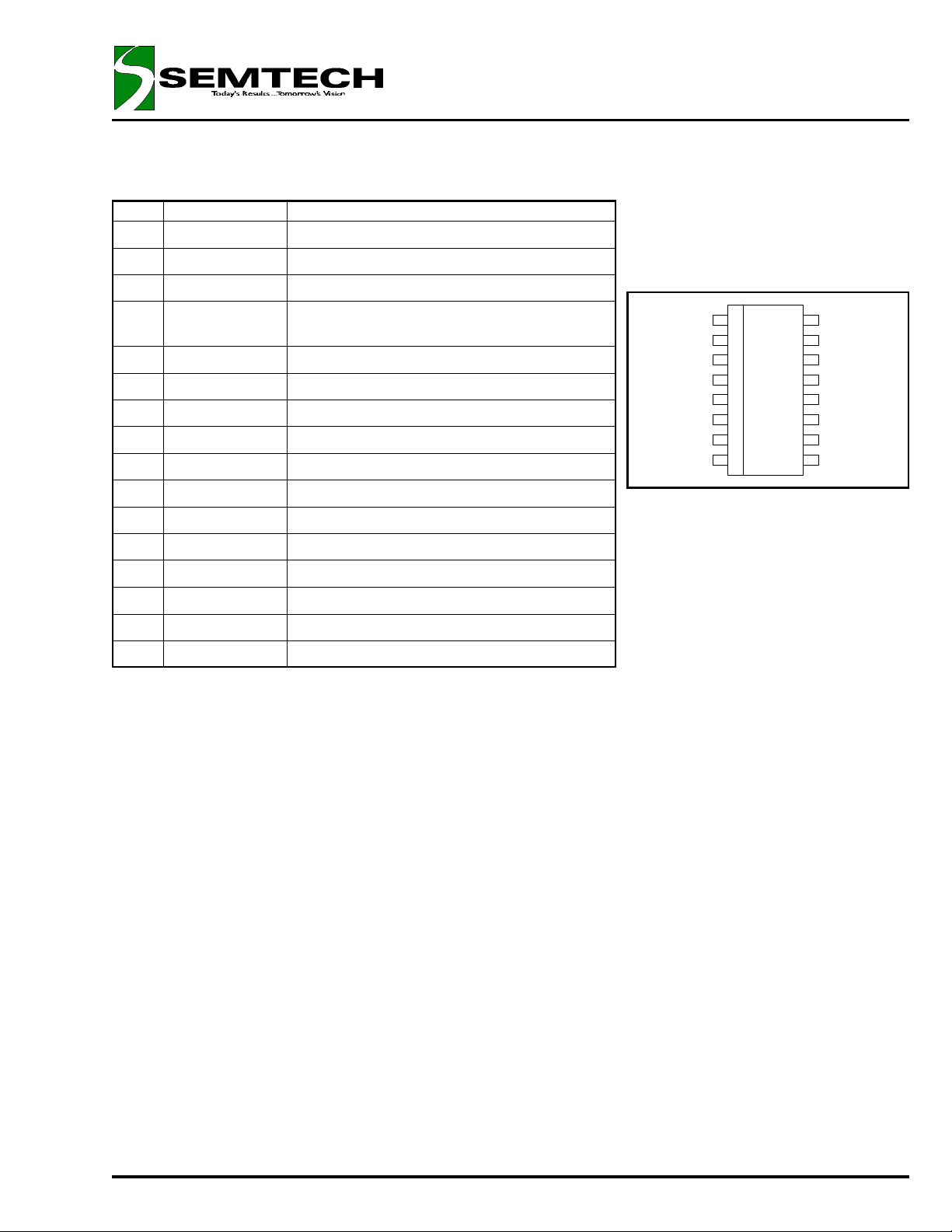
PIN DESCRIPTION
Pin # Pin Name Pin Function
GND
1
2
3
4
5
6
7
8
9
10
11
12
13
14
15
16
V
CC
OVP
PWRGOOD
CSm
CSp
PGND
DH
BST
SHUTDOWN
V
OSENSE
(1)
VID4
(1)
VID3
(1)
VID2
(1)
VID1
(1)
VID0
(1)
(1)
Small Signal Analog and Digital Ground
Chip Supply Voltage
High Signal out if VO>setpoint + 20%
Open collector logic output, high if VO within
10% of setpoint
Current Sense Input (negative)
Current Sense Input (positive)
Power Ground
High Side Driver Output
Vcc for High Side Driver
Logic low shuts down the converter
Top end of internal feedback chain
Programming Input (MSB)
Programming Input
Programming Input
Programming Input
Programming Input (LSB)
PROGRAMMABLE DC/DC CONTROLLER
FOR ADVANCED MICROPROCESSORS
GND
VCC
OVP
PWRGOOD
CSm
CSp
1
2
3
4
5
6
7
8
16
15
14
13
12
11
10
9
SC1151
VID0
VID1
VID2
VID3
VID4
VOSENSE
SHUTDOWNPGND
BSTDH
NOTE:
(1) All logic level inputs and outputs are
open collector TTL compatible
3

© 1998 SEMTECH CORP.
652 MITCHELL ROAD NEWBURY PARK CA
March 11, 1998
APPLICATION CIRCUIT
PROGRAMMABLE DC/DC CONTROLLER
FOR ADVANCED MICROPROCESSORS
SC1151
5V IN
0.1uF
Q1
BUK556
+
C3
C2
1000uF
1000uF
+
C4
1000uF
12V IN
OVP
VID0
VID1
VID2
VID3
VID4
SHUTDOWN
PWRGD
C1
R2
+
10k
R5
10
2
3
16
15
14
13
10
1
U1
VCC
OVP
VID0
VID1
VID2
VID3
SHUTDOWN
GND
SC1151CS
C13
0.1uF
VOSENSE
PWRGOOD
CSp
CSm
VID4
BST
PGND
D1
PSR16C30CT
6
5
11
4
12
9
8
DH
7
L1
4uH
R3 2.32k
C11
0.1uF
R4
1.00k
R1
5mOhm
+
C5
1000uF
REF 16935F
C6
1000uF
C8
1000uF
+
+
C7
1000uF
C10
1000uF
+
+
C9
1000uF
+
C12
0.1uF
VCCP
MATERIALS LIST
Quantity Reference Part/Description Vendor Notes
4 C1,C11-C13 0.1µF Ceramic Various
9 C2-C10 1000µF/6.3V SANYO MV-GX or equiv. Low ESR
1 D1 PSR16C30CT PHOTRON
1 L1 4µH 8 Turns 16AWG on MICROMETALS T50-52D core
1 Q1 BUK556 PHILIPS
1 R1
1 R2
1 R3
1 R4
1 R5
5mΩ
10kΩ, 5%, 1/8W
2.32kΩ, 1%, 1/8W
1kΩ, 1%, 1/8W
10Ω, 5%, 1/8W
IRC OAR-1 Series
Various
Various
Various
Various
1 U1 SC1151CS SEMTECH
Logic level FET, ≤22mΩ, 30V
4

© 1998 SEMTECH CORP.
652 MITCHELL ROAD NEWBURY PARK CA
March 11, 1998
CHARACTERISTIC CURVES
PROGRAMMABLE DC/DC CONTROLLER
FOR ADVANCED MICROPROCESSORS
SC1151
SC1151 Efficiency in Application circuit 16935F
100.0%
95.0%
90.0%
85.0%
Efficiency
80.0%
75.0%
70.0%
0.0 2.0 4.0 6.0 8.0 10.0 12.0
Output Current (Amps)
3.50V Set
3.00V Set
2.40V Set
2.00V Set
Application circuit 16935F Transient Response, 3.1V, 0.3A to 10A
Vo at Io=300mA steady state
Application circuit 16935F Ripple, 3.1V, 10A out
14.0
SC1151 Regulation in Application circuit 16935F
0.050
0.040
0.030
Vo at Io=10A steady state
Steady state voltage
levels are superimposed
for reference.
0.020
0.010
0.000
Voltage change (V) normalized at Io=2A
-0.010
-0.020
0.0 2.0 4.0 6.0 8.0 10.0 12.0 14.0
Output Current (Amps)
5

© 1998 SEMTECH CORP.
652 MITCHELL ROAD NEWBURY PARK CA
March 11, 1998
OUTLINE DRAWING SO-16
PROGRAMMABLE DC/DC CONTROLLER
FOR ADVANCED MICROPROCESSORS
SC1151
LAND PATTERN SO-16
6
 Loading...