

Absolute Maximum Ratings
GB
SEMITRANS 3
Ω
case
1)
= 25 °C
Symbol Conditions
V
CES
V
CGR
I
C
I
CM
V
GES
P
tot
Tj, (T
V
isol
humidity
climate
RGE = 20 k
T
case
T
case
per IGBT, T
)
stg
AC, 1 min.
DIN 40040
DIN IEC 68 T.1
= 25/80 °C
= 25/80 °C; tp = 1 ms
Values
1200
1200
150 / 100
300 / 200
–40 ... +150 (125)
Class F
40/125/56
4)
4)
± 20
1040
2500
Inverse Diode
= –I
I
F
IFM = –I
I
FSM
I2t
T
C
CM
= 25/80 °C
case
= 25/80 °C; tp = 1 ms
T
case
t
= 10 ms; sin.; Tj = 150 °C
p
= 10 ms; Tj = 150 °C
t
p
115 / 80
300 / 200
1000
5000
Characteristics
CESTj
= 600 V
= R
Goff
2)
2)
1)
= 125 °C
Ω
= 10
min. typ. max. Units
≥
V
CES
4,5
–
–
–
–
–
51
–
–
–
–
–
3)
–
–
–
–
–
–
–
–
–
2)
2)
–
–
–
–
–
–
–
5,5
0,2
9
–
5,4(4,2)
6,7(5,3)
–
–
11,7
1000
720
–
110
50
360
40
13
3
2,0(1,8)
2,25(2,1)
–
8
35(50)
5(14)
–
–
–
–
6,5
2
–
1
8(6,5)
–
–
700
15,6
1600
1080
20
–
–
–
–
–
–
2,5
–
1,2
11
–
–
0,12
0,25
0,038
Symbol Conditions
V
(BR)CES
V
GE(th)
I
CES
I
GES
V
CEsat
V
CEsat
g
fs
C
CHC
C
ies
C
oes
C
res
L
CE
t
d(on)
t
r
t
d(off)
t
f
E
on
E
off
Inverse Diode
VF = V
VF = V
V
TO
r
t
I
RRM
Q
rr
Thermal ch aracteristics
R
thjc
R
thjc
R
thch
5)
Not suitable for hard switching using PWM: Use range “SKM ... 123D “or “...124D“
VGE = 0, IC = 2 mA
= VCE, IC = 2 mA
V
GE
= 0 Tj = 25 °C
V
GE
V
= V
CE
= 20 V, VCE = 0
V
GE
= 100 A VGE = 15 V;
I
C
I
= 150 A Tj = 25 (125) °C
C
= 20 V, IC = 100 A
V
CE
per IGBT
V
= 0
GE
= 25 V
V
CE
f = 1 MHz
V
CC
= –15 V / +15 V
V
GE
IC = 100 A, ind. load
R
Gon
Tj = 125 °C
8)
IF = 100 A VGE = 0 V;
EC
= 150 A Tj = 25 (125) °C
I
EC
F
T
= 125 °C
j
Tj = 125 °C
IF = 100 A; Tj = 25 (125) °C
IF = 100 A; Tj = 25 (125) °C
per IGBT
per diode
per module
Units
V
V
A
A
V
W
°C
V
A
A
A
A2s
V
V
mA
mA
µ
A
V
V
S
pF
nF
pF
pF
nH
ns
ns
ns
ns
mWs
mWs
V
V
V
Ω
m
A
µ
C
°C/W
°C/W
°C/W
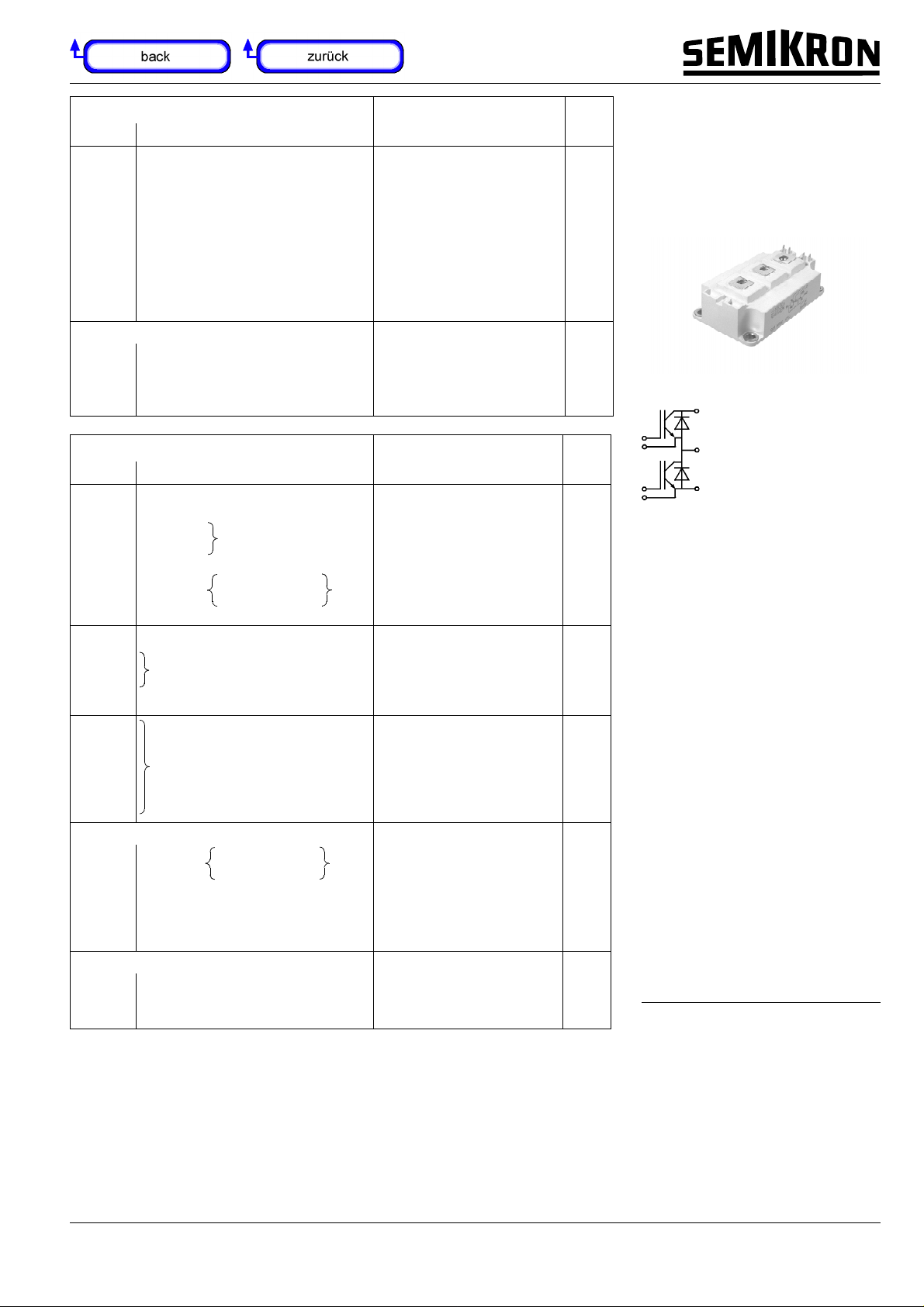
SEMITRANS® M
Ultra Fast IGBT Modules
SKM 150 GB 125 D
Preliminary Data
Features
•
N channel, homogeneous Silicon
structure (NPT- Non punchthrough IGBT)
•
Ultra fast with heavy metal
doping
•
Low inductance case
•
Almost no tail current
•
High short circuit capability,
4)
self limiting to 6 * I
•
Latch-up free
•
Fast & soft inverse CAL diodes
•
Isolated copper baseplate using
DCB Direct Copper Bonding
Technology
•
Large clearance (12 mm) and
creepage distances (20 mm)
Typical Applications
•
Fast switching (not for linear use)
•
High frequency welding
•
Induction heating
•
Resonant inverters (CSI, ZV, ZC)
•
Uninterruptable power supplies
> 20 kHz
1)
T
= 25 °C, unless otherwise
case
specified
2)
IF = – IC, VR = 600 V,
/dt = 1000 A/µs, VGE = 0 V
–di
F
3)
Use V
4)
GEoff
For paralleling use derating of 20 %
because of neg. temp. coefficient of
, contact factory, Subject to
V
CEsat
change
8)
CAL = Controlled Axial Lifetime
Technology.
Cases and mech. data
B 6 – 286
→
5)
cnom
= –5... –15 V
8)
© by SEMIKRON 0898 B 6 – 281
SKM 150 GB 125 D
1000
W
800
600
400
200
P
tot
0
0 20 40 60 80 100 120 140 160
T
C
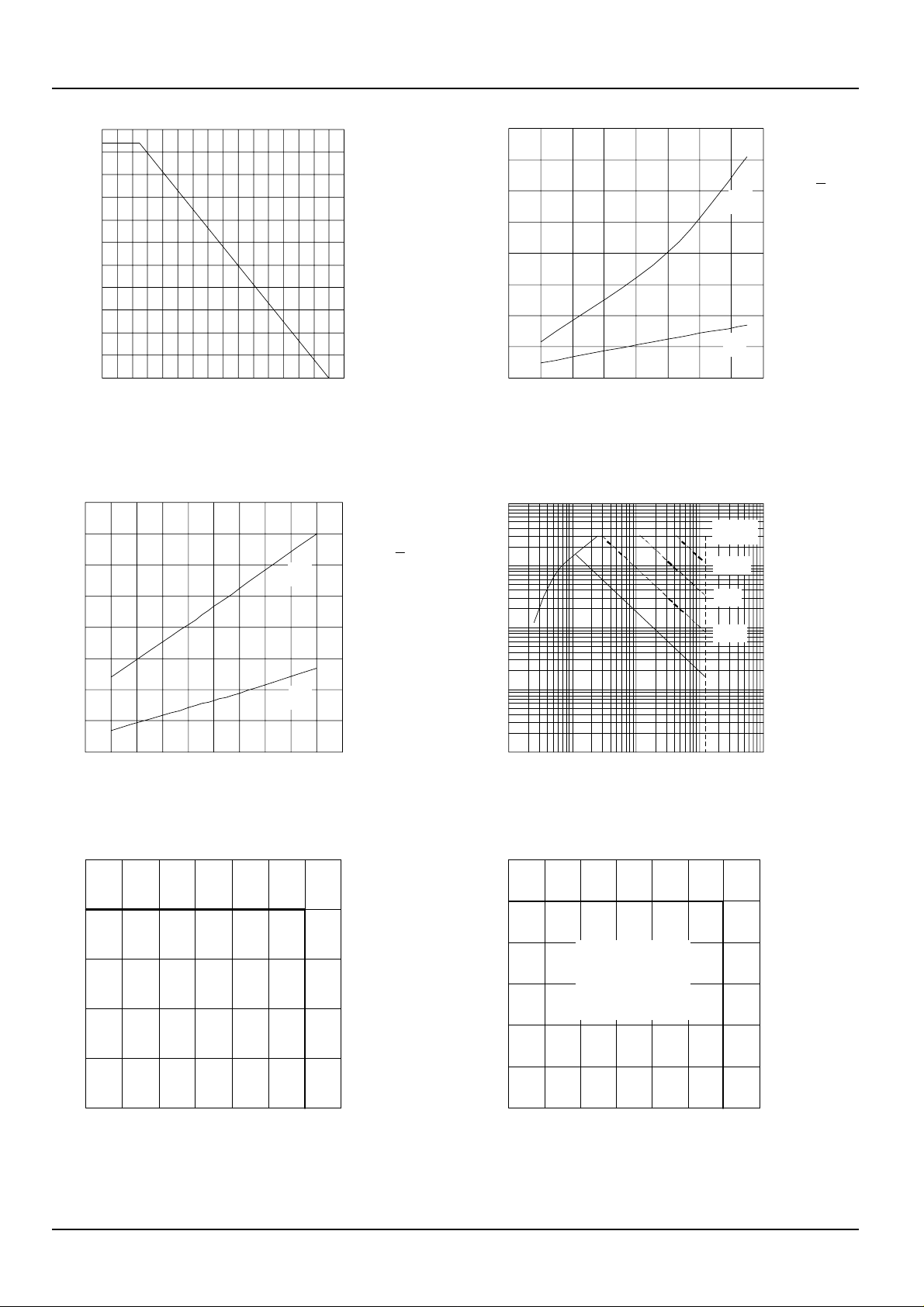
Fig. 1 Rated power dissipation P
40
mWs
30
M151GB12.XLS-1
°
C
= f (TC) Fig. 2 Turn-on /-off energy = f (IC)
tot
M151GB12.XLS-3
= 125 °C
T
j
V
= 600 V
CE
= + 15 V
V
GE
I
= 100 A
E
on
C
40
mWs
30
20
10
E
0
0 50 100 150 200
I
C
1000
A
100
M151GB12.XLS-2
E
on
E
off
A
M151GB12.XLS-4
tp=10µs
100µs
1ms
T
= 125 °C
j
= 600 V
V
CE
= + 15 V
V
GE
R
= 10
G
1 pulse
= 25 °C
T
C
Tj
150 °C
≤
Ω
20
10
E
0
0 1020304050
R
G
E
off
Ω
10
1
I
C
0,1
1 10 100 1000 10000
V
CE
10ms
Not for
linear use!
V
Fig. 3 Turn-on /-off ener gy = f (RG) Fig. 4 Maximum safe operat ing area (SOA) IC = f (VCE)
2,5
2
1,5
1
0,5
puls/IC
0
0 200 400 600 800 1000 1200 1400
V
CE
M151GB12.XLS-5
V
Tj
150 °C
≤
= 15 V
V
GE
R
= 10
Goff
IC = 100 A
Ω
12
10
8
6
4
2
I
CSC/IC
0
0 200 400 600 800 1000 1200 1400
V
CE
Note:
*Allowed numbers of
short circuits: <1000
*Time between short
circuits: >1s
Fig. 5 Turn-off safe operating area (RBSOA) Fig. 6 Safe operating area at short circuit I
M151GB12.XLS-6
V
Tj
150 °C
≤
= ± 15 V
V
GE
tsc
10 µs
≤
L < 25 nH
I
= 100 A
C
Use active
gate clamping
by Zene r diod e
16 V
R
= 6,8
Gmin
= f (VCE)
C
Ω
0898
© by SEMIKRONB 6 – 282

M151GB12.XLS-8
160
A
140
120
100
80
60
40
I
20
C
0
0 20 40 60 80 100 120 140 160
T
C
°C
T
= 150 °C
j
≥ 15V
V
GE
300
A
270
240
210
180
150
120
90
60
30
I
C
0
17V
15V
13V
11V
9V
7V
0246810
V
CE
M151GB12.XLS-9
V
Fig. 8 Rated current vs. temperature I
300
A
270
240
210
180
150
120
90
60
30
I
C
0
17V
15V
13V
11V
9V
7V
0246810
V
CE
= f (TC)
C
M151GB12.XLS-10
V
Fig. 9 Typ. output character istic, tp = 80 µs; 25 °C Fig. 10 Typ. output characteristic, tp = 80 µs; 125 °C
M151GB12.XLS-12
P
= V
cond(t)
V
V
typ.: r
max.: r
= V
CEsat(t)
CE(TO)(Tj)
CE(Tj)
CE(Tj)
valid for V
· I
CEsat(t)
CE(TO)(Tj)
C(t)
+ r
CE(Tj)
· I
C(t)
≤ 3,2 – 0,007 (Tj –25) [V]
= 0,020 + 0,00007 (Tj –25) [Ω]
≤ 0,047 – 0,00008 (Tj –25) [Ω]
= + 15 [V]; IC > 0,3 I
GE
+2
–1
Cnom
300
A
270
240
210
180
150
120
90
60
30
I
C
0
02468101214
V
GE
V
Fig. 11 Saturation characteristic (IGBT)
Calculation elements and equations Fig. 12 Typ. transfer characteristic, t
© by SEMIKRON B 6 – 2830898
= 80 µs; VCE = 20 V
p

SKM 150 GB 125 D
20
V
18
16
14
12
10
8
6
4
2
V
GE
0
0 200 400 600 800
Q
Gate
600V
M151GB12.XLS-13
800V
nC
I
Cpuls
= 100 A
100
nF
10
1
C
0,1
0 102030
V
CE
Fig. 13 Typ. gate charge characteristic Fig. 14 Typ. capacitances vs.V
M151GB12.XLS-15
1000
ns
100
= 125 °C
T
j
= 600 V
V
CE
V
= ± 15 V
GE
= 10
R
t
doff
t
don
t
r
t
f
t
Gon
R
Goff
induct. load
= 10
Ω
Ω
10000
ns
1000
100
t
M151GB12.XLS-14
V
CE
M151GB12.XLS-16
C
ies
C
oes
C
res
t
doff
t
don
t
r
t
f
VGE = 0 V
f = 1 MHz
T
= 125 °C
j
V
= 600 V
CE
= ± 15 V
V
GE
I
= 100 A
C
induct. load
10
0 50 100 150 200 250
I
C
Fig. 15 Typ. switching times vs. I
200
A
T
=125°C Tj=25°C
150
100
50
I
F
0
01234
V
j
F
A
C
M151GB12.XLS-17
V
10
0 204060
R
G
Ω
Fig. 16 Typ. switching times vs. gate resistor R
8
mJ
6
4
2
E
offD
0
0 50 100 150 200
I
F
M150GB12.XLS-18
RG=
Ω
5
Ω
8
Ω
13
Ω
25
50 Ω
A
G
V
V
CC
CC
= 125 °C
= 125 °C
T
T
j
j
V
V
GE
GE
Fig. 17 Typ. CAL diode forward characteristic Fig. 18 Diode turn-off energy dissipation per pulse
= 600 V
= 600 V
= ± 15 V
= ± 15 V
0898
© by SEMIKRONB 6 – 284

A
K/W
1
M151GB12.XLS-19
1
K/W
M151GB12.XLS-20
0,1
D=0,50
0,01
0,001
t
p
single pulse
Z
thJC
0,0001
1E-05 0,0001 0,001 0,01 0,1 1 10
0,20
0,10
0,05
0,02
0,01
s
Fig. 19 Transient thermal impedance of IGBT
= f (tp); D = tp / tc = tp · f
Z
thJC
150
A
100
M150GB12.XLS-22
RG=
Ω
5
Ω
8
V
= 600 V
CC
T
= 125 °C
j
= ± 15 V
V
GE
0,1
D=0,5
0,01
0,001
single pulse
Z
thJC
0,0001
1E-05 0,0001 0,001 0,01 0,1 1 10
t
p
Fig. 20 Transient thermal impedance of
inverse CAL diodes Z
150
A
100
= f (tp); D = tp / tc = tp · f
thJC
M150GB12.XLS-23
Ω
8
0,2
0,1
0,05
0,02
0,01
R
G
5
s
= 600 V
V
CC
T
= 125 °C
j
=
Ω
= ± 15 V
V
GE
I
= 100A
F
Ω
13
50
Ω
25
I
RR
0
0 50 100 150 200
I
F
50 Ω
A
Fig. 22 Typ. CAL diode peak reverse recov ery
current I
= f (IF; RG)
RR
Typical Applications
include
Switched mode power supplies
Inverters for high frequency
Inductive heating
UPS Uninterruptable power supplies
Electronic (also po rtable) welders
Pulse frequencies above 20 kHz ... 100kHz
Resona nt in ve rter s
Zero voltage switching (ZVS)
Zero current switching (ZCS)
Ω
13
50
I
RR
0
0 1000 2000 3000 4000
di
dt
/
F
50
Ω
25
Ω
A/µs
Fig. 23 Typ. CAL diode peak reverse recovery
current IRR = f (diF/dt)
30
µC
20
50 Ω
10
Q
rr
0
0 1000 2000 3000 4000
diF/dt
25
13 Ω
Ω
8 Ω
25 A
Fig. 24 Typ. CAL diode recovered charge Q
M150GB12.XLS-24
RG= 5
75 A
50 A
Ω
A/µs
I F =
150
100
rr
= 600 V
V
CC
= 125 °C
T
j
V
= ± 15 V
GE
= f (di/dt)
© by SEMIKRON B 6 – 2850898

SKM 150 GB 125 D
SEMITRANS 3
Case D 56
UL Recognized
File no. E 63 532
SKM 150 GB 125 D
Dimensions in mm
Case outline and circuit diagram
Mechanical Data
Symbol Conditions
M
1
M
2
a
w
to heatsink, SI Units (M6)
to heatsink, US Units
for terminals, SI Units (M6)
for terminals, US Units
Values Units
min. typ. max.
3
27
2,5
22
–
–
–
–
–
–
–
–
5
44
5
44
5x9,81
325
0898
Nm
lb.in.
Nm
lb.in.
m/s
g
This is an electrostatic discharge
sensitive device (ESDS).
Please observe the international
standard IEC 747-1, Chapter IX.
Three devices are supplied in one
SEM IB O X B w i thout mount ing
hardware, which can be ordered
2
separately under Ident No.
33321100 (for 10 SEMITRANS 3).
Larger packing units of 12 and 20
pieces are used if suitable
Accessories
SEM IB O X
→
→
B 6 - 4.
C - 1.
© by SEMIKRONB 6 – 286
 Loading...