

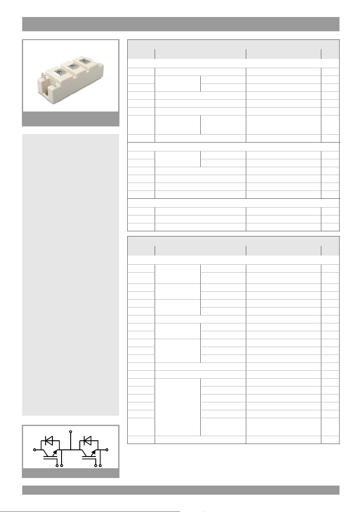
SKM100GB12V
SEMITRANS® 2
SKM100GB12V
Features
• V-IGBT = 6. Generation Trench V-IGBT
(Fuji)
• CAL4 = Soft switching 4. Generation
CAL-diode
• Isolated copper baseplate using DBC
technology (Direct Copper Bonding)
• UL recognized, file no. E63532
• Increased power cycling capability
• With integrated gate resistor
• Low switching losses at high di/dt
Typical Applications*
•AC inverter drives
•UPS
• Electronic welders
Remarks
• Case temperature limited to
T
= 125°C max, recomm.
c
T
= -40 ... +150°C, product
op
rel. results valid for T
= 150°
j
Absolute Maximum Ratings
Symbol Conditions Values Unit
IGBT
V
I
C
I
Cnom
I
CRM
V
CES
GES
Tj=25°C
Tj= 175 °C
I
= 3xI
CRM
Cnom
T
=25°C
c
T
=80°C
c
1200 V
159 A
121 A
100 A
300 A
-20 ... 20 V
VCC= 720 V
V
t
psc
T
j
GE
V
CES
≤ 20 V
≤ 1200 V
=125°C
T
j
10 µs
-40 ... 175 °C
Inverse diode
T
I
F
I
Fnom
I
FRM
I
FSM
T
Tj= 175 °C
I
= 3xI
FRM
Fnom
tp= 10 ms, sin 180°, Tj=25°C
j
=25°C
c
T
=80°C
c
121 A
91 A
100 A
300 A
550 A
-40 ... 175 °C
Module
T
I
t(RMS)
T
stg
V
isol
terminal
=80°C
200 A
-40 ... 125 °C
AC sinus 50Hz, t = 1 min 4000 V
Characteristics
Symbol Conditions min. typ. max. Unit
IGBT
V
CE(sat)
V
CE0
r
CE
V
GE(th)
I
CES
C
ies
C
oes
C
res
Q
R
Gint
t
d(on)
t
r
E
on
t
d(off)
t
f
E
off
R
th(j-c)
IC=100A
V
=15V
GE
chiplevel
VGE=15V
VGE=VCE, IC= 4 mA 5.5 6 6.5 V
VGE=0V
V
= 1200 V
CE
VCE=25V
V
=0V
GE
G
VGE= - 8 V...+ 15 V
VCC= 600 V
I
=100A
C
V
=±15V
GE
R
=1
G on
R
=1
G off
di/dt
= 3230 A/µs
on
di/dt
=1330A/µs
off
du/dt
= 9350 V/
off
µs
per IGBT 0.27 K/W
T
=25°C
j
=150°C
T
j
Tj=25°C
T
=150°C
j
T
=25°C
j
T
=150°C
j
T
=25°C
j
T
=150°C
j
f=1MHz
f=1MHz
f=1MHz
T
=150°C
j
Tj=150°C
Tj=150°C
Tj=150°C
Tj=150°C
Tj=150°C
1.75 2.20 V
2.20 2.50 V
0.94 1.04 V
0.88 0.98 V
8.10 11.6 m
13.20 15.20 m
0.1 0.3 mA
mA
6.01 nF
0.59 nF
0.589 nF
1150 nC
7.5
294 ns
38 ns
10.7 mJ
418 ns
62 ns
8.7 mJ
GB
© by SEMIKRON Rev. 5 – 23.03.2011 1

SKM100GB12V
SEMITRANS® 2
SKM100GB12V
Features
• V-IGBT = 6. Generation Trench V-IGBT
(Fuji)
• CAL4 = Soft switching 4. Generation
CAL-diode
• Isolated copper baseplate using DBC
technology (Direct Copper Bonding)
• UL recognized, file no. E63532
• Increased power cycling capability
• With integrated gate resistor
• Low switching losses at high di/dt
Characteristics
Symbol Conditions min. typ. max. Unit
Inverse diode
V
V
r
F
I
RRM
Q
E
R
= V
F
F0
rr
rr
th(j-c)
IF= 100 A
EC
V
=0V
GE
chip
IF= 100 A
di/dt
=3050A/µs
off
V
=±15V
GE
V
= 600 V
CC
per diode 0.48 K/W
T
=25°C
j
=150°C
T
j
Tj=25°C
T
=150°C
j
Tj=25°C
T
=150°C
j
T
=150°C
j
Tj=150°C
Tj=150°C
2.20 2.52 V
2.15 2.47 V
1.3 1.5 V
0.9 1.1 V
9.0 10.2 m
12.5 13.7 m
90 A
15 µC
5.7 mJ
Module
L
CE
R
CC'+EE'
R
th(c-s)
M
s
M
t
terminal-chip
T
C
T
=125°C
C
0.65 m
1m
=25°C
per module 0.04 0.05 K/W
to heat sink M6 3 5 Nm
to terminals M5
2.5 5 Nm
30 nH
Nm
w 160 g
Typical Applications*
•AC inverter drives
•UPS
• Electronic welders
Remarks
• Case temperature limited to
T
= 125°C max, recomm.
c
T
= -40 ... +150°C, product
op
rel. results valid for T
= 150°
j
GB
2 Rev. 5 – 23.03.2011 © by SEMIKRON

SKM100GB12V
Fig. 1: Typ. output characteristic, inclusive R
Fig. 3: Typ. turn-on /-off energy = f (IC) Fig. 4: Typ. turn-on /-off energy = f (RG)
CC'+ EE'
Fig. 2: Rated current vs. temperature IC = f (TC)
Fig. 5: Typ. transfer characteristic Fig. 6: Typ. gate charge characteristic
© by SEMIKRON Rev. 5 – 23.03.2011 3

SKM100GB12V
Fig. 7: Typ. switching times vs. I
C
Fig. 8: Typ. switching times vs. gate resistor R
G
Fig. 9: Transient thermal impedance Fig. 10: Typ. CAL diode forward charact., incl. R
CC'+EE'
Fig. 11: CAL diode peak reverse recovery current Fig. 12: Typ. CAL diode peak reverse recovery charge
4 Rev. 5 – 23.03.2011 © by SEMIKRON

SKM100GB12V
SEMITRANS 2
GB
This is an electrostatic discharge sensitive device (ESDS), international standard IEC 60747-1, Chapter IX
* The specifications of our components may not be considered as an assurance of component characteristics. Components have to be tested
for the respective application. Adjustments may be necessary. The use of SEMIKRON products in life support appliances and systems is
subject to prior specification and written approval by SEMIKRON. We therefore strongly recommend prior consultation of our staff.
© by SEMIKRON Rev. 5 – 23.03.2011 5
 Loading...