

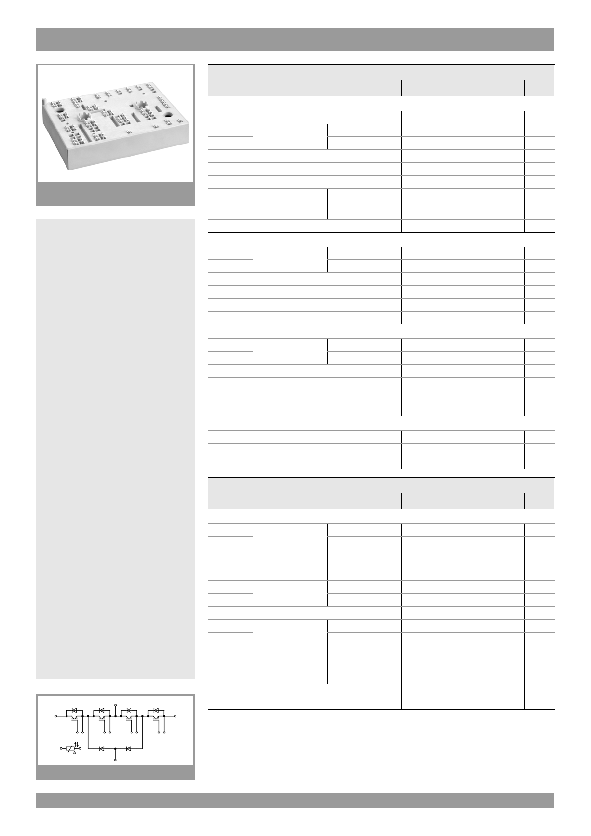
SKiiP 39MLI07E3V1
MiniSKiiP® 3
3-Level NPC Inverter
SKiiP 39MLI07E3V1
Features
•650V Trench IGBTs
• Robust and soft diodes in CAL
technology
• Highly reliable spring contacts for
electrical connections
• UL recognised: File no. E63532
Typical Applications*
• Uninterruptible power supplies (UPS)
•Solar inverters
Remarks
• Case temperature limited to TC = 125°C
max.; T
modules)
• Product reliability results valid for
T
T
= TS (valid for baseplateless
C
≤150°C (recommended
j
=-40…+150°C)
op
Absolute Maximum Ratings
Symbol Conditions Values Unit
IGBT
V
I
C
I
Cnom
I
CRM
V
CES
GES
Tj= 175 °C
I
= 2 x I
CRM
Cnom
T
=25°C
s
T
=70°C
s
650 V
159 A
125 A
200 A
400 A
-20 ... 20 V
VCC= 360 V
V
t
psc
T
j
GE
V
CES
≤ 15 V
≤ 650 V
=150°C
T
j
6µs
-40 ... 175 °C
Inverse diode
T
I
F
I
Fnom
I
FRM
I
FSM
T
Tj= 175 °C
I
= 2 x I
FRM
Fnom
tp= 10 ms, sin 180°, Tj=25°C
j
=25°C
s
T
=70°C
s
163 A
125 A
200 A
400 A
1470 A
-40 ... 175 °C
Clamping diode
T
I
F
I
Fnom
I
FRM
I
FSM
T
Tj= 175 °C
I
= 2xI
FRM
Fnom
10 ms, sin 180°, Tj= 25 °C 1470 A
j
=25°C
s
T
=70°C
s
163 A
125 A
200 A
400 A
-40 ... 175 °C
Module
T
I
t(RMS)
T
stg
V
isol
= 80°C, 20A per spring
terminal
200 A
-40 ... 125 °C
AC sinus 50 Hz, t = 1 min 2500 V
Characteristics
Symbol Conditions min. typ. max. Unit
IGBT
V
CE(sat)
V
CE0
r
CE
V
GE(th)
I
CES
C
ies
C
oes
C
res
Q
R
Gint
IC=200A
V
=15V
GE
chiplevel
chiplevel
VGE=15V
chiplevel
VGE=VCE, IC=3.2mA
VGE=0V
V
= 650 V
CE
VCE=25V
V
=0V
GE
G
VGE= - 8 V...+ 15 V
Tj=25°C
T
=25°C
j
=150°C
T
j
T
=25°C
j
T
=150°C
j
T
=25°C
j
T
=150°C
j
T
=25°C
j
f=1MHz
f=1MHz
f=1MHz
1.45 1.85 V
1.70 2.10 V
0.9 1 V
0.85 0.9 V
2.8 4.3 mΩ
4.3 6 mΩ
55.86.5V
0.1 0.3 mA
mA
12.34 nF
0.77 nF
0.37 nF
1600 nC
2 Ω
MLI
© by SEMIKRON Rev. 0 – 02.04.2014 1
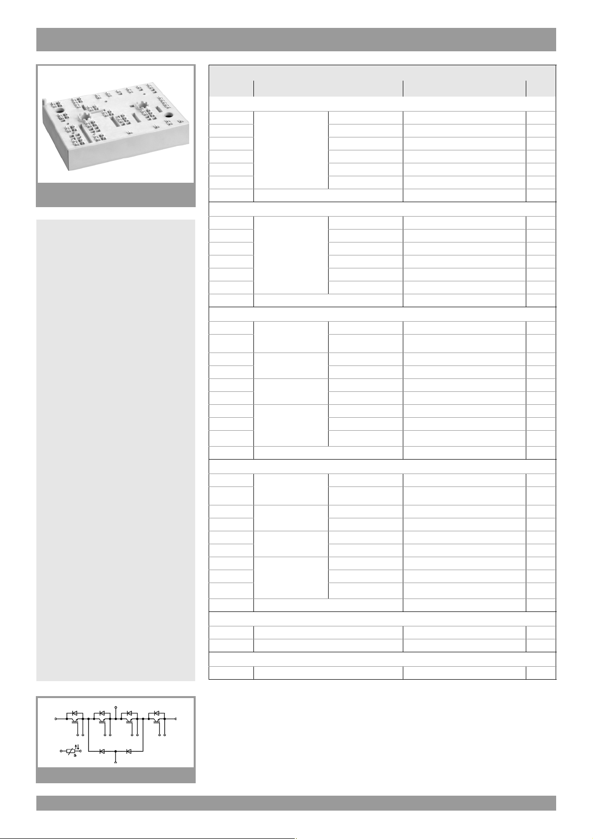
SKiiP 39MLI07E3V1
MiniSKiiP® 3
3-Level NPC Inverter
SKiiP 39MLI07E3V1
Features
•650V Trench IGBTs
• Robust and soft diodes in CAL
technology
• Highly reliable spring contacts for
electrical connections
• UL recognised: File no. E63532
Typical Applications*
• Uninterruptible power supplies (UPS)
•Solar inverters
Remarks
• Case temperature limited to TC = 125°C
max.; T
modules)
• Product reliability results valid for
T
T
= TS (valid for baseplateless
C
≤150°C (recommended
j
=-40…+150°C)
op
Characteristics
Symbol Conditions min. typ. max. Unit
T1 / T4
T
t
d(on)
t
r
E
t
d(off)
t
f
E
R
on
off
th(j-s)
VCE= 300 V
I
=200A
C
V
= +15/-15 V
GE
R
=2Ω
G on
R
=2Ω
G off
di/dt
= 3150 A/µs
on
di/dt
=2000A/µs
off
per IGBT 0.5 K/W
=150°C
j
Tj=150°C
Tj=150°C
Tj=150°C
Tj=150°C
Tj=150°C
165 ns
69 ns
3.6 mJ
341 ns
83 ns
8.9 mJ
T2 / T3
T
t
d(on)
t
r
E
t
d(off)
t
f
E
R
on
off
th(j-s)
VCE= 300 V
I
=200A
C
V
= +15/-15 V
GE
R
=2Ω
G on
R
=2Ω
G off
di/dt
= 3120 A/µs
on
di/dt
=2000A/µs
off
=150°C
j
Tj=150°C
Tj=150°C
Tj=150°C
Tj=150°C
Tj=150°C
152 ns
70 ns
1.8 mJ
324 ns
89 ns
9.5 mJ
0.5 K/W
Inverse diode
V
V
r
F
I
RRM
Q
E
R
= V
F
F0
rr
rr
th(j-s)
IF= 200 A
EC
V
=0V
GE
chiplevel
chiplevel
chiplevel
IF= 200 A
di/dt
=2700A/µs
off
V
=-15V
GE
per Diode 0.6 K/W
T
=25°C
j
=150°C
T
j
=25°C
T
j
T
=150°C
j
T
=25°C
j
T
=150°C
j
=150°C
T
j
Tj=150°C
Tj=150°C
1.4 1.8 V
1.4 1.8 V
11.2V
0.9 1 V
1.8 2.6 mΩ
2.6 3.9 mΩ
157 A
31 µC
8.3 mJ
Clamping diode
V
V
r
F
I
RRM
Q
E
R
= V
F
F0
rr
rr
th(j-s)
IF= 200 A
EC
V
=0V
GE
chiplevel
chiplevel
chiplevel
IF= 200 A
di/dt
=3100A/µs
off
V
=-15V
GE
per Diode 0.6 K/W
T
=25°C
j
=150°C
T
j
T
=25°C
j
T
=150°C
j
T
=25°C
j
T
=150°C
j
=150°C
T
j
Tj=150°C
Tj=150°C
1.4 1.8 V
1.4 1.8 V
11.2V
0.9 1 V
1.8 2.6 mΩ
2.6 3.9 mΩ
171 A
16 µC
4mJ
Module
M
s
to heat sink 2 2.5 Nm
wweight 82 g
Temperature Sensor
R
25
NTC, Tr = 25 °C
1)
5.0 ± 5% kΩ
MLI
2 Rev. 0 – 02.04.2014 © by SEMIKRON

SKiiP 39MLI07E3V1
Fig. 1: Typ. output characteristic, inclusive R
Fig. 3: Typ. turn-on /-off energy = f (IC) Fig. 4: Typ. turn-on /-off energy = f (RG)
CC'+ EE'
Fig. 2: Rated current vs. temperature IC = f (TS)
Fig. 5: Typ. transfer characteristic Fig. 6: Typ. gate charge characteristic
© by SEMIKRON Rev. 0 – 02.04.2014 3

SKiiP 39MLI07E3V1
Fig. 7: Typ. switching times vs. I
Fig. 9: Transient thermal impedance of IGBT and Diode Fig. 10: CAL diode forward characteristic
C
Fig. 8: Typ. switching times vs. gate resistor R
G
Fig. 11: Typ. CAL diode peak reverse recovery current Fig. 12: Typ. CAL diode recovery charge
4 Rev. 0 – 02.04.2014 © by SEMIKRON

SKiiP 39MLI07E3V1
pinout, dimensions
pinout
This is an electrostatic discharge sensitive device (ESDS), international standard IEC 60747-1, Chapter IX
* The specifications of our components may not be considered as an assurance of component characteristics. Components have to be tested
for the respective application. Adjustments may be necessary. The use of SEMIKRON products in life support appliances and systems is
subject to prior specification and written approval by SEMIKRON. We therefore strongly recommend prior consultation of our staff.
© by SEMIKRON Rev. 0 – 02.04.2014 5
 Loading...