

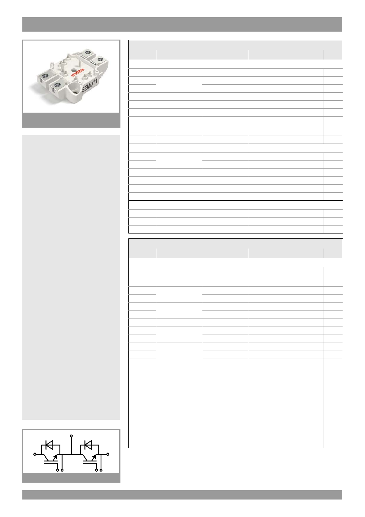
SEMiX151GB12Vs
SEMiX® 1s
SEMiX151GB12Vs
Features
• Homogeneous Si
•V
• High short circuit capability
• UL recognised file no. E63532
Typical Applications*
•AC inverter drives
•UPS
• Electronic Welding
Remarks
• Case temperature limited to TC=125°C
• Product reliability results are valid for
with positive temperature
CE(sat)
coefficient
max.
T
=150°C
j
Absolute Maximum Ratings
Symbol Conditions Values Unit
IGBT
V
I
C
I
Cnom
I
CRM
V
CES
GES
Tj=25°C
Tj= 175 °C
I
= 3xI
CRM
Cnom
T
=25°C
c
T
=80°C
c
1200 V
231 A
176 A
150 A
450 A
-20 ... 20 V
VCC= 720 V
V
t
psc
T
j
GE
V
CES
≤ 15 V
≤ 1200 V
=125°C
T
j
10 µs
-40 ... 175 °C
Inverse diode
T
I
F
I
Fnom
I
FRM
I
FSM
T
Tj= 175 °C
I
= 3xI
FRM
Fnom
tp= 10 ms, sin 180°, Tj=25°C
j
=25°C
c
T
=80°C
c
189 A
141 A
150 A
450 A
900 A
-40 ... 175 °C
Module
T
I
t(RMS)
T
stg
V
isol
terminal
=80°C
600 A
-40 ... 125 °C
AC sinus 50Hz, t = 1 min 4000 V
Characteristics
Symbol Conditions min. typ. max. Unit
IGBT
V
CE(sat)
V
CE0
r
CE
V
GE(th)
I
CES
C
ies
C
oes
C
res
Q
R
Gint
t
d(on)
t
r
E
on
t
d(off)
t
f
E
off
R
th(j-c)
IC=150A
V
=15V
GE
chiplevel
chiplevel
VGE=15V
chiplevel
VGE=VCE, IC= 6 mA 5.5 6 6.5 V
VGE=0V
V
= 1200 V
CE
VCE=25V
V
=0V
GE
G
VGE= - 8 V...+ 15 V
Tj=25°C
VCC= 600 V
I
=150A
C
V
=±15V
GE
R
=1
G on
R
=1
G off
di/dt
= 4600 A/µs
on
di/dt
=1700A/µs
off
du/dt
= 6700 V/
off
µs
per IGBT 0.19 K/W
T
=25°C
j
=150°C
T
j
T
=25°C
j
T
=150°C
j
T
=25°C
j
T
=150°C
j
T
=25°C
j
T
=150°C
j
f=1MHz
f=1MHz
f=1MHz
T
=150°C
j
Tj=150°C
Tj=150°C
Tj=150°C
Tj=150°C
Tj=150°C
1.75 2.20 V
2.20 2.50 V
0.94 1.04 V
0.88 0.98 V
5.4 7.7 m
8.8 10.1 m
0.1 0.3 mA
mA
9.0 nF
0.89 nF
0.88 nF
1650 nC
5.00
319 ns
46 ns
19.4 mJ
482 ns
68 ns
17.1 mJ
GB
© by SEMIKRON Rev. 4 – 13.12.2012 1
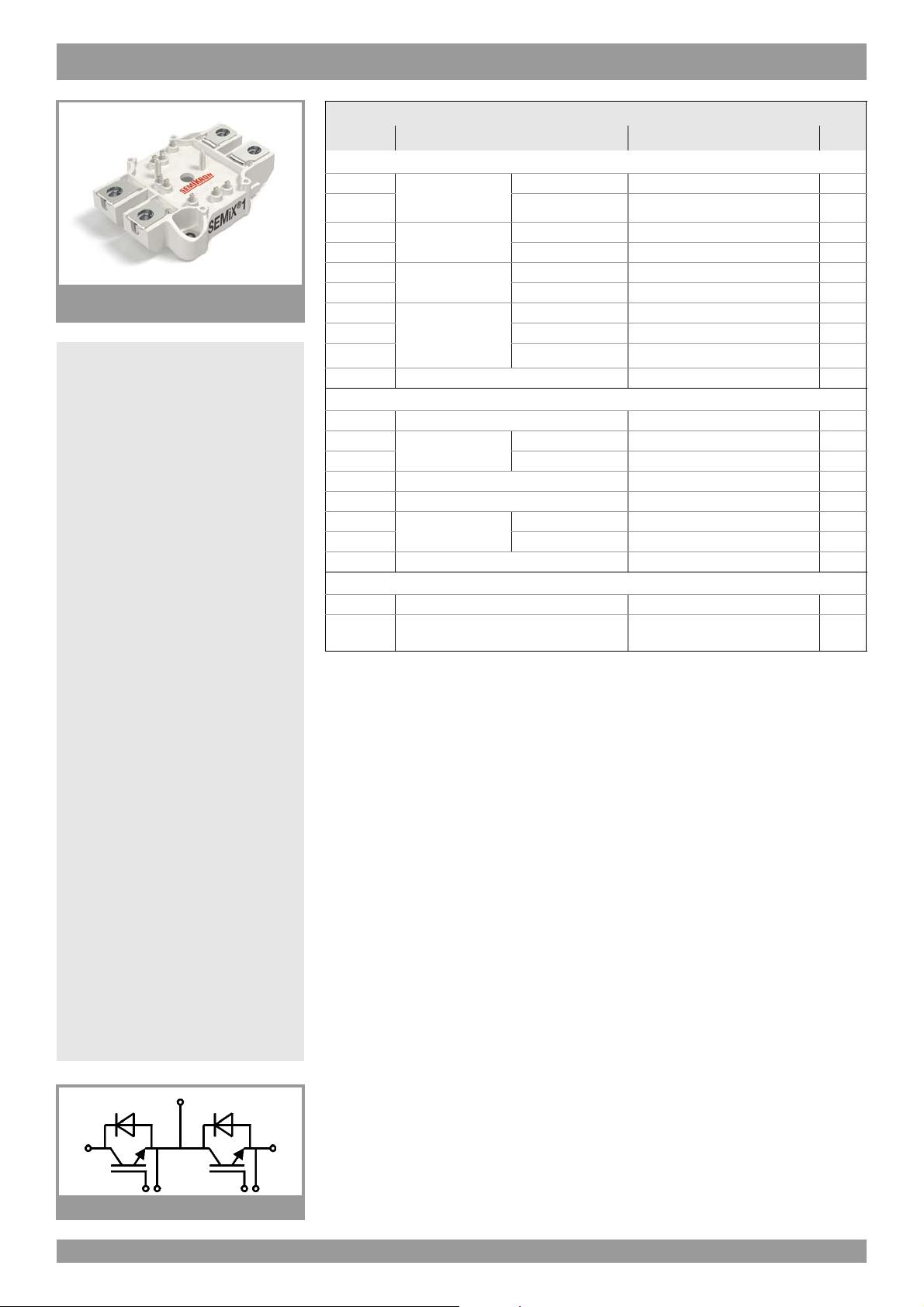
SEMiX151GB12Vs
SEMiX® 1s
SEMiX151GB12Vs
Features
• Homogeneous Si
•V
• High short circuit capability
• UL recognised file no. E63532
Typical Applications*
•AC inverter drives
•UPS
• Electronic Welding
Remarks
• Case temperature limited to TC=125°C
• Product reliability results are valid for
with positive temperature
CE(sat)
coefficient
max.
T
=150°C
j
Characteristics
Symbol Conditions min. typ. max. Unit
Inverse diode
V
V
r
F
I
RRM
Q
E
R
= V
F
F0
rr
rr
th(j-c)
IF= 150 A
EC
V
=0V
GE
chiplevel
chiplevel
chiplevel
IF= 150 A
di/dt
=4400A/µs
off
V
=-15V
GE
V
= 600 V
CC
per diode 0.31 K/W
T
=25°C
j
=150°C
T
j
=25°C
T
j
T
=150°C
j
T
=25°C
j
T
=150°C
j
T
=150°C
j
Tj=150°C
Tj=150°C
2.14 2.46 V
2.07 2.38 V
1.1 1.3 1.5 V
0.7 0.9 1.1 V
4.3 5.6 6.4 m
7.0 7.8 8.5 m
175 A
27.5 µC
11.5 mJ
Module
L
CE
R
CC'+EE'
R
th(c-s)
M
s
M
t
=25°C
T
res., terminal-chip
C
T
=125°C
C
per module 0.075 K/W
to heat sink (M5) 3 5 Nm
to terminals (M6)
2.5 5 Nm
16 nH
0.7 m
1m
Nm
w145g
Temperatur Sensor
R
100
B
100/125
Tc=100°C (R25=5 k) 493 ± 5%
R
(T)=R100
exp[B
100/125
(1/T-1/T
100
)]; T[K];
3550
±2%
K
GB
2 Rev. 4 – 13.12.2012 © by SEMIKRON

SEMiX151GB12Vs
Fig. 1: Typ. output characteristic, inclusive R
Fig. 3: Typ. turn-on /-off energy = f (IC) Fig. 4: Typ. turn-on /-off energy = f (RG)
CC'+ EE'
Fig. 2: Rated current vs. temperature IC = f (TC)
Fig. 5: Typ. transfer characteristic Fig. 6: Typ. gate charge characteristic
© by SEMIKRON Rev. 4 – 13.12.2012 3

SEMiX151GB12Vs
Fig. 7: Typ. switching times vs. I
C
Fig. 8: Typ. switching times vs. gate resistor R
G
Fig. 9: Typ. transient thermal impedance Fig. 10: Typ. CAL diode forward charact., incl. R
CC'+ EE'
Fig. 11: Typ. CAL diode peak reverse recovery current Fig. 12: Typ. CAL diode recovery charge
4 Rev. 4 – 13.12.2012 © by SEMIKRON

SEMiX151GB12Vs
SEMiX 1s
spring configuration
This is an electrostatic discharge sensitive device (ESDS), international standard IEC 60747-1, Chapter IX
* The specifications of our components may not be considered as an assurance of component characteristics. Components have to be tested
for the respective application. Adjustments may be necessary. The use of SEMIKRON products in life support appliances and systems is
subject to prior specification and written approval by SEMIKRON. We therefore strongly recommend prior consultation of our staff.
© by SEMIKRON Rev. 4 – 13.12.2012 5
 Loading...