Semiconductor Components NCS21801, NCS21802, NCS21803, NCS21804 Datasheet
Precision Operational
Amplifier, 10 mV, Zero-Drift,
1.6 V to 5.5 V Supply,
1.5 MHz
NCS21801, NCS21802,
NCS21803, NCS21804
The NCS21801, NCS21802, NCS21803, and NCS21804 are
precision op amps featuring low input offset voltage and low offset
drift over time and temperature. The common mode voltage range
extends 100 mV beyond the supply rails, which makes it suitable for
both high−side and low−side current sensing applications.
The NCS2180x is available in single, dual, and quad channel
configurations. All versions are specified for operation from −40°C to
+125°C. NCV prefix parts are automotive grade 1 qualified and offer
performance over the extended temperature range from −40°C to
+150°C.
Features
• Input Offset Voltage: ±10 mV max
• Offset Voltage Drift Over Temperature: ±5 nV/°C Typical
• Common Mode Input Voltage Range: V
• Supply Voltage Range: 1.8 V to 5.5 V
• Extended Supply Voltage Range: 1.6 V to 5.5 V for T
• Unity Gain Bandwidth: 1.5 MHz
• Quiescent Consumption: 100 mA Max per Channel
• Enable Function Available on NCS21803
• NCV Prefix for Automotive and Other Applications Requiring
Unique Site and Control Change Requirements; AEC−Q100
Qualified and PPAP Capable
• These Devices are Pb−Free, Halogen Free/BFR Free and are RoHS
Compliant
Applications
• High−Side Current Sensing
• Low−Side Current Sensing
• Difference Amplifier
• Instrumentation Amplifier
• Power Management
• Automotive
– 0.1 V to VDD + 0.1 V
SS
= 0°C to 85°C
A
www.onsemi.com
5
1
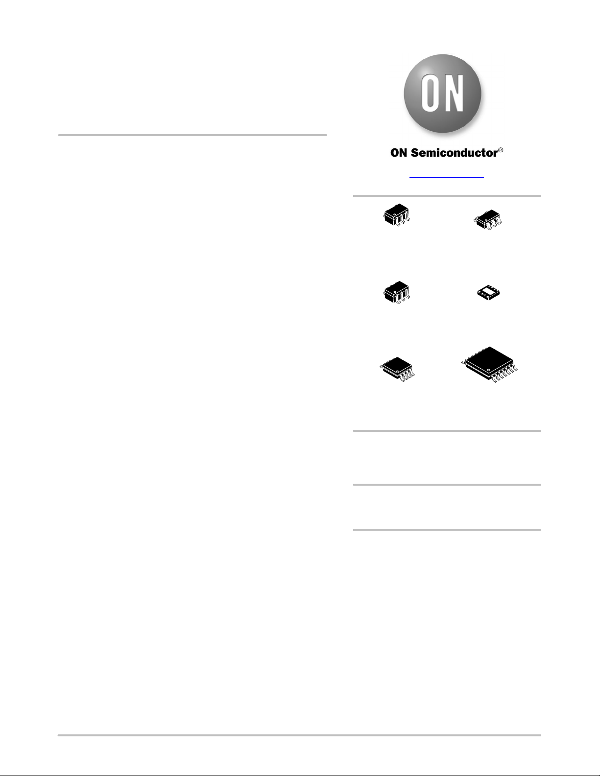
SC−88A / SC70−5
CASE 419A−02
1
SC−88 / SC70−6
CASE 419B−02
1
Micro8
CASE 846A−02
DEVICE MARKING INFORMATION
See general marking information in the device marking
section on page 2 of this data sheet.
PIN CONNECTIONS
See pin connections on page 3 of this data sheet.
ORDERING INFORMATION
See detailed ordering and shipping information on page 2 of
this data sheet.
5
1
TSOP−5 / SOT23−5
CASE 483
1
UDFN8
CASE 517AW
14
1
TSSOP−14 WB
CASE 948G
© Semiconductor Components Industries, LLC, 2020
April, 2021 − Rev. 2
1 Publication Order Number:
NCS21801/D
NCS21801, NCS21802, NCS21803, NCS21804
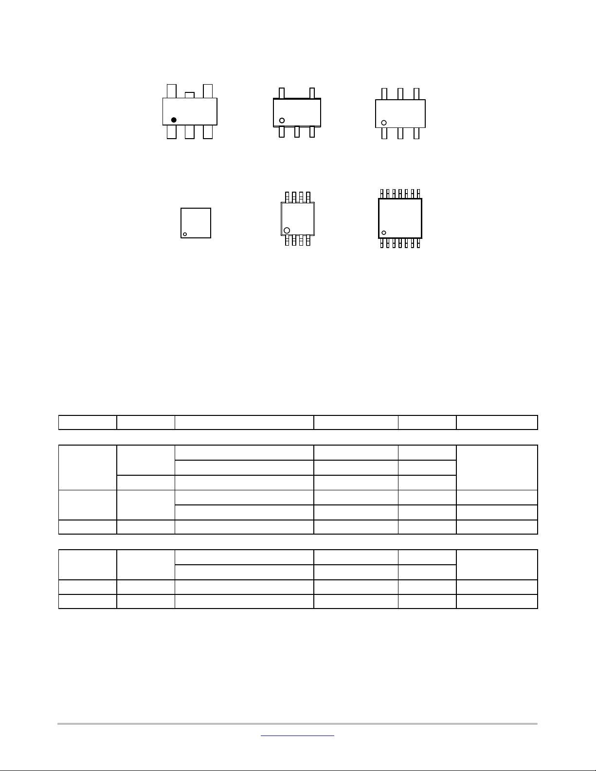
DEVICE MARKING INFORMATION
6
ACC\A/(YW)G
G
TSOP−5 / SOT23−5
CASE 483
AAJ
YM
1
UDFN8, 2x2, 0.5P
CASE 517AW
AAU(M)G
G
SC−88A / SC70−5
CASE 419A−02
8
802
AYW G
G
1
Micro8
CASE 846A−02
XX = Specific Device Code
A = Assembly Location
Y = Year
W = Work Week
M = Date Code
G or G = Pb−Free Package
(Note: Microdot may be in either location)
SC−88 / SC70−6 / SOT−363
AAE(M)G
G
1
CASE 419B−02
14
804
ALYWG
G
1
TSSOP−14 WB
CASE 948G
ORDERING INFORMATION
Channels Enable Package Part Number Marking Shipping
INDUSTRIAL AND CONSUMER
Single
Dual No
Quad No TSSOP−14 NCS21804DTBR2G** 804 2500 / Tape & Reel
AUTOMOTIVE QUALIFIED
Single
Dual No Micro8 NCV21802DMR2G 802 4000 / Tape & Reel
Quad No TSSOP−14 NCV21804DTBR2G** 804 2500 / Tape & Reel
†For information on tape and reel specifications, including part orientation and tape sizes, please refer to our Tape and Reel Packaging
Specifications Brochure, BRD8011/D.
** In development. Contact local sales office for more information.
No
Yes SC−88 / SC70−6 / SOT−363 NCS21803SQT2G** AAE
No
SOT23−5 / TSOP−5 NCS21801SN2T1G** ACC
SC70−5 / SC−88−5 / SOT−353−5 NCS21801SQ3T2G** AAU
UDFN−8 NCS21802MUTBG AAJ 3000 / Tape & Reel
Micro8 NCS21802DMR2G 802 4000 / Tape & Reel
SOT23−5 / TSOP−5 NCV21801SN2T1G** ACC
SC70−5 / SC−88−5 / SOT−353−5 NCV21801SQ3T2G** AAU
3000 / Tape & Reel
3000 / Tape & Reel
www.onsemi.com
2
NCS21801, NCS21802, NCS21803, NCS21804
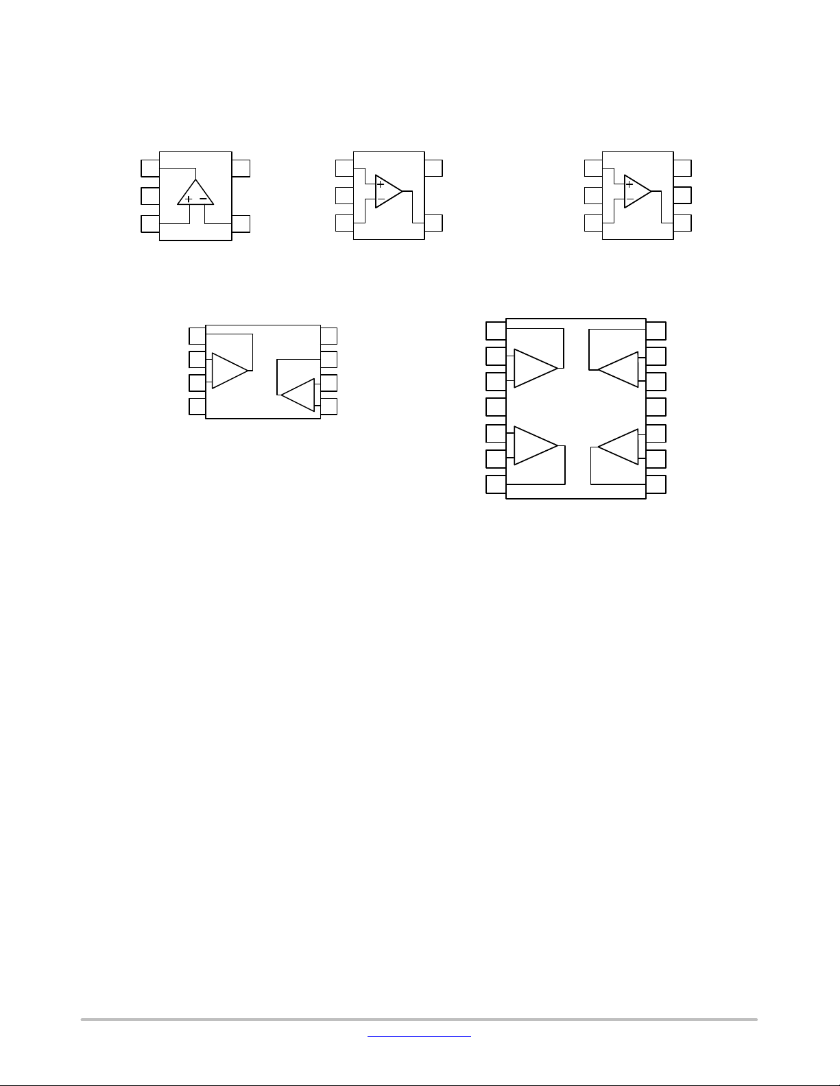
PIN CONNECTIONS
OUT
VSS
IN+
Single Channel Configuration
1
2
34
SOT23−5 / TSOP−5
Dual Channel Configuration
OUT 1
IN− 1
IN+ 1
VSS
1
−
2
+
3
4
UDFN8 / Micro8
NCS21801
VDD
5
IN−
NCS21802
IN+
VSS
IN−
SC70−5 / SC−88−5 / SOT−353−5
−
+
1
5
VDD
2
34
8
VDD
7
OUT 2
6
IN− 2
IN+ 2
5
OUT
OUT 1
IN− 1
IN+ 1
VDD
IN+ 2
IN− 2
OUT 2
Single Channel with Enable Configuration
IN+
VSS
IN−
Quad Channel Configuration
NCS21804
1
2
−
+
3
4
5
+
−
6
7
TSSOP−14
NCS21803
1
2
34
SC88 / SC70−6 / SOT−363
14
13
−
+
12
11
10
+
−
9
8
6
VDD
5
EN
OUT
OUT 4
IN− 4
IN+ 4
VSS
IN+ 3
IN− 3
OUT 3
www.onsemi.com
3
NCS21801, NCS21802, NCS21803, NCS21804
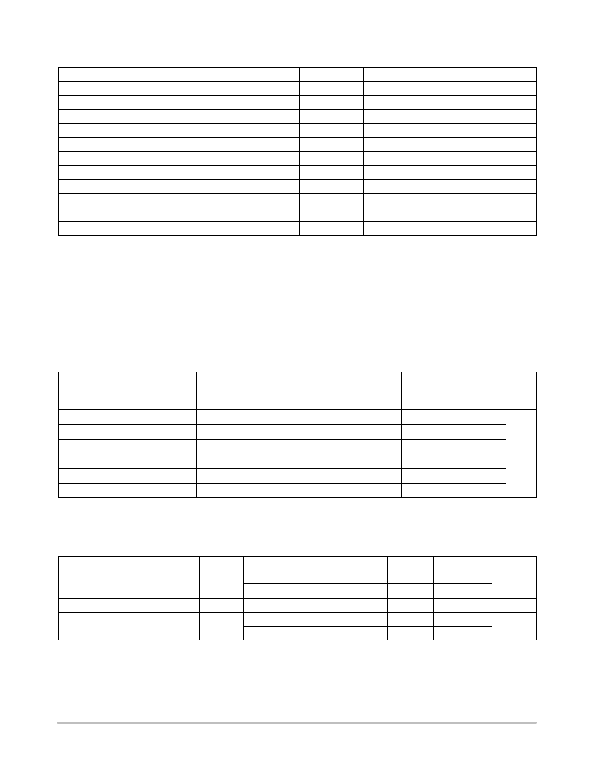
MAXIMUM RATINGS (Note 1)
Parameter
Supply Voltage (VDD − VSS) (Note 1) V
Input Voltage (Note 2) V
Differential Input Voltage V
Output Voltage (Note 2) V
Output Short Circuit Current (Note 3) I
Input Current into Any Pin (Note 2) I
Maximum Junction Temperature T
Storage Temperature Range T
ESD Human Body Model (Note 4) HBM ±2000 V
Charged Device Model (Note 4) CDM ±1000 V
Latch−up Current (Note 5) 100 mA
Stresses exceeding those listed in the Maximum Ratings table may damage the device. If any of these limits are exceeded, device functionality
should not be assumed, damage may occur and reliability may be affected.
1. Refer to ELECTRICAL CHARACTERISTICS, RECOMMENDED OPERATING RANGES and/or APPLICATION INFORMATION for safe
operating parameters
2. Terminals are diode−clamped to the power−supply rails. Input signals that can swing more than 0.3 V beyond the supply rails should be
current limited to ±10 mA or less. Output terminals should not be driven by external sources.
3. Short circuits to either rail can cause an increase in the junction temperature. The total power dissipation must be limited to prevent the
junction temperature from exceeding the 150°C limit.
4. This device series incorporates ESD protection and is tested by the following methods:
ESD Human Body Model tested per JEDEC standard JS−001−2017 (AEC−Q100−002)
ESD Charged Device Model tested per JEDEC standard JS−002−2014 (AEC−Q100−011)
5. Latch−up Current tested per JEDEC standard: JESD78E.
Symbol Rating Unit
S
IN+,VIN−,
IN+,VIN−
OUT
OUT
IN
J(max)
STG
V
EN
−0.3 to 6 V
(VSS − 0.3) to (VDD + 0.3) V
± (VDD – VSS + 0.3) V
(VSS − 0.3) to (VDD + 0.3) V
Continuous
±10 mA
+150 °C
−65 to +150 °C
THERMAL CHARACTERISTICS (Notes 6, 7)
q
JA
Package
Junction−to−Ambient
Thermal Resistance
Junction−to−Case Top
Thermal Characteristic
TSOP−5 / SOT23−5 188 26 38
SC70−5 / SC−88−5 / SOT−353−5 241 46 64
SC−88 / SC70−6 / SOT−363 230 45 60
UDFN8 105 10 51
Micro8 / MSOP−8 105 24 96
TSSOP−14 86 9 53
6. Refer to ELECTRICAL CHARACTERISTICS, RECOMMENDED OPERATING RANGES and/or APPLICATION INFORMATION for safe
operating parameters
7. Mounted on a JESD51−7 thermal board, 2S2P, 1 in
2
copper spreader area, 1 oz signal plane thickness
Y
JT
Y
JB
Junction−to−Board
Thermal Characteristic
Unit
°C/W
RECOMMENDED OPERATING RANGES
Parameter Symbol Conditions Min Max Unit
Ambient Temperature T
A
NCS prefix −40 125
NCV prefix −40 150 (Note 8)
Common Mode Input Voltage V
Supply Voltage (VDD − VSS) V
CM
S
Full temperature range VSS – 0.1 VDD + 0.1 V
TA = 0 to 85°C 1.6 5.5
Full temperature range 1.8 5.5
Functional operation above the stresses listed in the Recommended Operating Ranges is not implied. Extended exposure to stresses beyond
the Recommended Operating Ranges limits may affect device reliability.
8. Operation up to T
the 150°C absolute maximum limit.
= 150°C is permitted, provided the total power dissipation is limited to prevent the junction temperature from exceeding
A
°C
V
www.onsemi.com
4
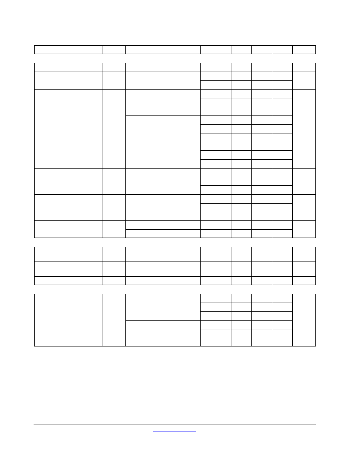
NCS21801, NCS21802, NCS21803, NCS21804
ELECTRICAL CHARACTERISTICS At T
= +25°C, Vs = 1.8 V to 5.5 V, and VCM = V
A
= mid−supply, unless otherwise noted.
OUT
Boldface limits apply over the specified temperature range, unless otherwise noted, guaranteed by characterization and/or design.
Parameter Symbol Conditions Temp (5C) Min Typ Max Unit
INPUT
Input Offset Voltage
Input Offset Voltage Drift vs.
V
dVOS/dT VS = 1.8 V to 5.5 V
Temperature
Common Mode Rejection Ratio CMRR VS = 1.8 V,
VS = 3.3 V 25 ±2 ±10
OS
–40 to 125 ±5 ±75
–40 to 150 ±5 ±75
25 106 131
= V
V
CM
− 0.1 V to VDD + 0.1 V
SS
–40 to 125 100
–40 to 150 100
VS = 3.3 V,
= V
V
CM
SS
− 0.1 V to VDD + 0.1 V
25 113 134
–40 to 125 110
–40 to 150 110
VS = 5.5 V,
V
= V
CM
SS
− 0.1 V to VDD + 0.1 V
25 111 137
–40 to 125 108
–40 to 150 108
Input Bias Current (Note 9) I
IB
25 ±60 ±200
–40 to 125 ±600
–40 to 150 ±5000
Input Offset Current
(Note 9)
I
OS
25 ±60 ±300
–40 to 125 ±400
–40 to 150 ±2500
Input Capacitance C
Differential 25 5
IN
Common mode 25 5
ENABLE (Note 10)
Input Voltage Low Threshold
V
EN−L
Shutdown –40 to 125 V
SS
+
0.5
Input Voltage High Threshold V
EN−H
Enabled –40 to 125 V
SS
+
1.3
Input Leakage Current I
EN
25 1 100 nA
OUTPUT CHARACTERISTICS
Open Loop Voltage Gain
A
VOL
VS = 1.8 V
25 108 133
–40 to 125 106
–40 to 150 106
VS = 3.3 V, 5.5 V
25 120 143
–40 to 125 110
–40 to 150 110
9. Guaranteed by characterization and/or design.
10.The enable function is available on NCS21803 only. The EN pin must be connected to a logic low or logic high voltage.
11.Shutdown Time (t
point at which the output voltage reaches within 10% of its final value.
) and Enable Time (tON) are defined as the time between the 50% point of the signal applied to the EN pin and the
OFF
mV
nV/°C
dB
pA
pA
pF
V
V
dB
www.onsemi.com
5
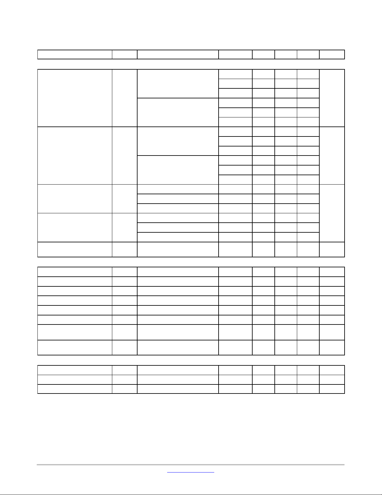
NCS21801, NCS21802, NCS21803, NCS21804
ELECTRICAL CHARACTERISTICS At T
= +25°C, Vs = 1.8 V to 5.5 V, and VCM = V
A
= mid−supply, unless otherwise noted.
OUT
Boldface limits apply over the specified temperature range, unless otherwise noted, guaranteed by characterization and/or design.
Parameter UnitMaxTypMinTemp (5C)ConditionsSymbol
OUTPUT CHARACTERISTICS
Output Voltage High,
Referenced from V
DD Supply
Rail
VDD −
V
OH
I
= 30 mA 25 1 5
OUT
–40 to 125 10
–40 to 150 10
VS = 3.3 V, I
OUT
= 3 mA
25 55 100
–40 to 125 125
–40 to 150 125
Output Voltage Low,
Referenced to V
SS Supply Rail
V
−
I
OL
V
SS
= 30 mA 25 1 5
OUT
–40 to 125 10
–40 to 150 10
VS = 3.3 V, I
OUT
= 3 mA
25 55 100
–40 to 125 125
–40 to 150 125
Output Current Sourcing
Capability
I
VS = 1.8 V 25 24
O
VS = 3.3 V 25 29
VS = 5.5 V 25 32
Output Current Sinking
Capability
I
VS = 1.8 V 25 28
O
VS = 3.3 V 25 32
VS = 5.5 V 25 38
Capacitive Load Capability C
AV = −1, VIN = 100 mVpp step
L
A
= 1, VIN = 100 mVpp step
V
25 400
125
DYNAMIC RESPONSE
Unity Gain Bandwidth
Gain Margin A
Phase Margin
BW CL = 20 pF 25 1.5 MHz
CL = 20 pF 25 6 dB
M
F
CL = 20 pF 25 50 °
M
Slew Rate SR 25 0.7
Settling Time t
Overload Recovery Time t
Channel Separation NCS21802, NCS21804,
0.1%, AV = 1 25 20
s
V
OR
* GAIN > V
IN
S
25 200
25 90 dB
f = 10 kHz
EMI Rejection Ratio EMIRR 25 See Fig.
26
NOISE
Voltage Noise Density
Voltage Noise, Peak−to−Peak e
Current Noise Density i
e
VS = 3.3, fin = 1 kHz 25 42 nV/√Hz
N
P−Pfin
N
= 0.1 Hz to 10 Hz 25 400 nV
fin = 1 kHZ 25 445 fA/√Hz
9. Guaranteed by characterization and/or design.
10.The enable function is available on NCS21803 only. The EN pin must be connected to a logic low or logic high voltage.
11.Shutdown Time (t
point at which the output voltage reaches within 10% of its final value.
) and Enable Time (tON) are defined as the time between the 50% point of the signal applied to the EN pin and the
OFF
mV
mV
mA
pF
V/ms
ms
ms
dB
PP
www.onsemi.com
6
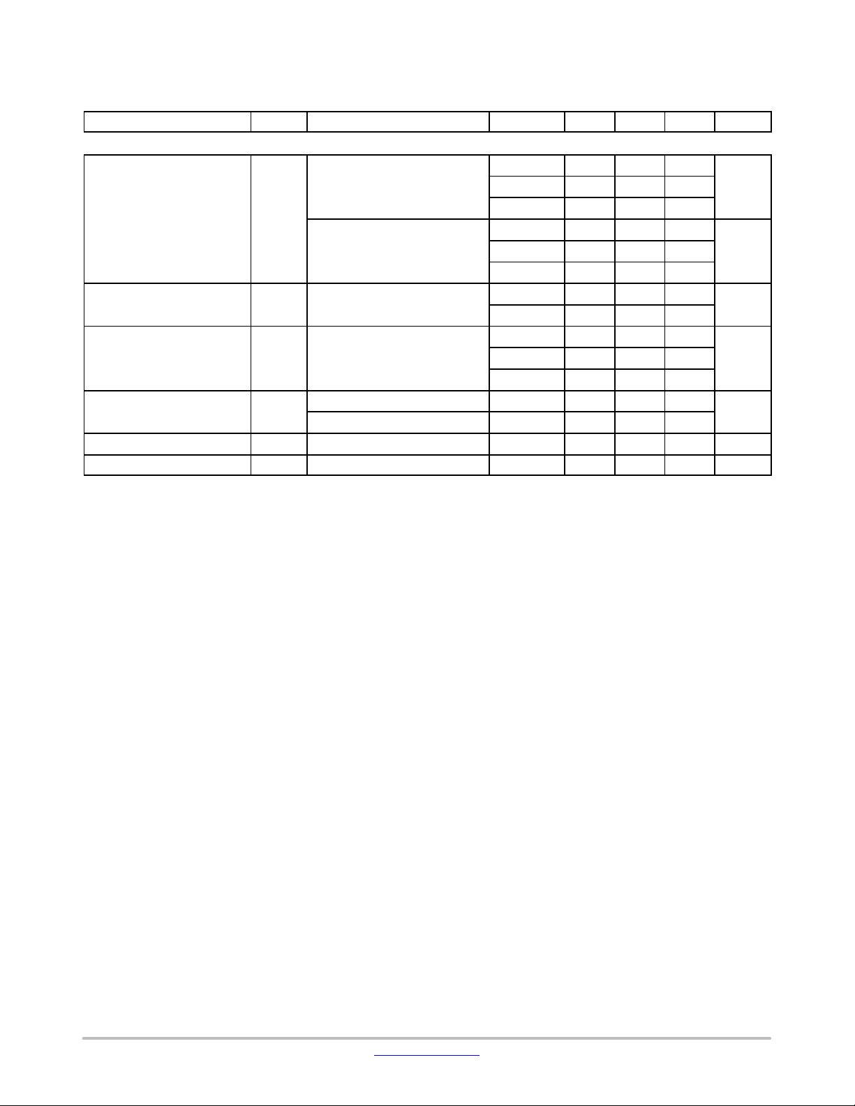
NCS21801, NCS21802, NCS21803, NCS21804
ELECTRICAL CHARACTERISTICS At T
= +25°C, Vs = 1.8 V to 5.5 V, and VCM = V
A
= mid−supply, unless otherwise noted.
OUT
Boldface limits apply over the specified temperature range, unless otherwise noted, guaranteed by characterization and/or design.
Parameter UnitMaxTypMinTemp (5C)ConditionsSymbol
POWER SUPPLY
Quiescent Current
I
NCS21801, NCS2803,
Q
no load
25 75 105 mA
–40 to 125 130
–40 to 150 200
NCS21802, NCS21804,
per channel, no load
25 75 100 mA
–40 to 125 125
–40 to 150 150
Quiescent Current in Shutdown
(Note 10)
Power Supply Rejection Ratio PSRR VS = 1.8 V to 5.5 V
I
QSD
Per channel
25 TBD 300
–40 to 85 300
25 115 140
nA
dB
–40 to 125 110
–40 to 150 110
Power Up Time
NCS21801 25 75 ms
NCS21802, NCS21804 25 40
Enable Time (Note 10, 11) t
Shutdown Time (Note 10, 11) t
ON
OFF
25 40
25 TBD
ms
ms
9. Guaranteed by characterization and/or design.
10.The enable function is available on NCS21803 only. The EN pin must be connected to a logic low or logic high voltage.
11.Shutdown Time (t
point at which the output voltage reaches within 10% of its final value.
) and Enable Time (tON) are defined as the time between the 50% point of the signal applied to the EN pin and the
OFF
Product parametric performance is indicated in the Electrical Characteristics for the listed test conditions, unless otherwise noted. Product
performance may not be indicated by the Electrical Characteristics if operated under different conditions.
www.onsemi.com
7

NCS21801, NCS21802, NCS21803, NCS21804
ELECTRICAL CHARACTERISTICS At T
limits apply over the specified temperature range, T
Parameter
Symbol Conditions Temp (5C) Min Typ Max Unit
= +25°C, VS = 1.6 V, and VCM = V
A
= 0°C to 85°C, guaranteed by characterization and/or design.
A
= mid−supply, unless otherwise noted. Boldface
OUT
INPUT
Input Offset Voltage
Input Offset Voltage Drift vs.
V
OS
dVOS/dT 0 to 85 ±5 ±75 nV/°C
25 ±3 ±13
Temperature
Common Mode Rejection Ratio CMRR VCM = V
− 0.1 V to VDD + 0.1 V
SS
25 96 123
0 to 85 94
Input Bias Current
(Note 12)
Input Offset Current
(Note 12)
Input Capacitance C
I
IB
25 ±30 ±160
0 to 85 ±250
I
OS
25 ±36 ±200
0 to 85 ±250
Differential 25 5
IN
Common mode 25 5
ENABLE (Note 14)
Input Voltage Low Threshold
Input Voltage High Threshold V
V
EN−L
EN−H
Shutdown 0 to 85 V
Enabled 0 to 85 V
SS
+
1.3
Input Leakage Current I
EN
25 1 100 nA
OUTPUT CHARACTERISTICS
Open Loop Voltage Gain A
VOL
25 106 128
0 to 85 104
Output Voltage High,
Referenced from V
Supply Rail
DD
VDD −
V
OH
I
= 30 mA 25 1 5
OUT
0 to 85 10
I
OUT
= 3 mA
25 85 130
0 to 85 150
Output Voltage Low,
Referenced to V
SS
Supply Rail
V
−
I
OL
V
SS
= 30 mA 25 1 5
OUT
0 to 85 10
I
OUT
= 3 mA
25 75 130
0 to 85 150
Output Current Sourcing
Capability
Output Current Sinking
Capability
Capacitive Load Capability C
I
o
I
o
AV = −1, VIN = 100 mVpp step
L
A
= 1, VIN = 100 mVpp step
V
25 15
25 21
25 400
125
DYNAMIC RESPONSE
Unity Gain Bandwidth
Gain Margin A
Phase Margin
BW CL = 20 pF 25 1.4 MHz
CL = 20 pF 25 6 dB
M
F
CL = 20 pF 25 50 °
M
Slew Rate SR 25 0.7
12.Guaranteed by design and/or characterization.
13.The enable function is available on NCS21803 only. The EN pin must be connected to a logic low or logic high voltage.
14.Shutdown Time (t
point at which the output voltage reaches within 10% of its final value.
) and Enable Time (tON) are defined as the time between the 50% point of the signal applied to the EN pin and the
OFF
SS
0.5
mV
dB
pA
pA
pF
+
V
V
dB
mV
mV
mA
pF
V/ms
www.onsemi.com
8
 Loading...