

Page 1
NCP81276
l
4/3/2/1 Phase Buck
Controller with PWM_VID
2
and I
C Interface
The NCP81276 is a multiphase synchronous controller optimized
for new generation computing and graphics processors. The device is
capable of driving up to 4 phases and incorporates differential voltage
and phase current sensing, adaptive voltage positioning and
PWM_VID interface to provide and accurately regulated power for
computer or graphic controllers. The integrated power saving
interface (PSI) allows for the processors to set the controller in one of
three modes, i.e. all phases on, dynamic phases shedding or fixed low
phase count mode, to obtain high efficiency in light-load conditions.
The dual edge PWM multiphase architecture ensures fast transient
response and good dynamic current balance.
Features
• Compliant with NVIDIA
®
OVR4+ Specifications
• Supports Up to 4 Phases
• 4.5 V to 20 V Supply Voltage Range
• 250 kHz to 1.2 MHz Switching Frequency (4 Phase)
• Power Good Output
• Under Voltage Protection (UVP)
• Over Voltage Protection (OVP)
• Over Current Protection (OCP)
• Per Phase Over Current Protection
• Startup into Pre-Charged Loads while Avoiding False OVP
• Configurable Adaptive Voltage Positioning (AVP)
• High Performance Operational Error Amplifier
• True Differential Current Balancing Sense Amplifiers for Each
Phase
• Phase-to-Phase Dynamic Current Balancing
• Current Mode Dual Edge Modulation for Fast Initial Response to
Transient Loading
• Power Saving Interface (PSI)
• Automatic Phase Shedding with User Settable Thresholds
• PWM_VID and I
2
C Control Interface
• Compact 40 Pin QFN Package (5 × 5 mm Body, 0.4 mm Pitch)
• This Device is Pb-Free and is RoHS Compliant
www.onsemi.com
401
QFN40
CASE 485CR
MARKING DIAGRAM
1
NCP81276 = Specific Device Code
A = Assembly Location
WL = Wafer Lot
YY = Year
WW = Work Week
G = Pb-Free Package
(Note: Microdot may be in either location)
ON
NCP
81276
AWLYYWWG
G
PIN CONNECTIONS
VSN
VCC
SDA
SCL
EN
PSI
PGOOD
VID_BUFF
REFIN
VREF
VRMP
OCP
LPC1
LPC2
PWM4/PHTH1
PWM3/PHTH2
PWM2/PHTH3
PWM_VID
40
38
39
1
2
3
4
SS
5
6
7
8
9
10
11
PHTH4
PWM1/
NCP81276
13
12
NCNCNC
DRON
35
36
37
(TOP VIEW )
Tab: GROUND
161514
NC
34
17
CSP4
33
18
CSP3
32
19
CSP2
VSP
31
20
CSP1
30
29
28
27
26
25
24
23
22
21
COMP
FB
DIFF
FSW
LLTH/I2C_ADD
IOUT
ILIM
CSCOMP
CSSUM
CSREF
Typical Applications
• GPU and CPU Power
• Graphic Cards
• Desktop and Notebook Applications
© Semiconductor Components Industries, LLC, 2017
September, 2017 − Rev. 10
ORDERING INFORMATION
Device Package Shipping
NCP81276MNTXG QFN40
5000/Tape & Ree
(Pb-Free)
†For information on tape and reel specifications,
including part orientation and tape sizes, please
refer to our Tape and Reel Packaging Specification
Brochure, BRD8011/D
.
1 Publication Order Number:
NCP81276/D
†
Page 2
VCC_DUT
TP51
TP50
TP49
TP48
TP47
TP46
TP45
VSN_sense
J4
R38
SDA
2.2R
C5
SCL
J3
C17
1000pF
EN
NCP81276
R125
R124
C21 470pF
R1260R
22
CSSUM
CSCOMP
PWM3/PHTH2
9
R57
26.1k
R56
10k
47k
R55
51k
R54
R1270R
220k
75k
R50
C13
21
41
CSREF
PWM2/PHTH3
10
36pF
RT1
390nF
PAD
CSP1
20
CSP2
19
CSP3
18
CSP4
17
NC
16
NC
15
NC
14
NC
13
DRON
12
PWM1/PHTH4
11
TP62
R22
68k
R18
33k
R14
1k
R13
1k
R10
10k
R7
10k
C19
R51
C20
1000pF
165k
DRON
TP60
10R
R45
10R
R44
C10 0.1uF
TP61
10R
R47
10R
R46
0.1uF
C11
0.1uF
C12
0.1uF
C14
2k32
2k32
2k32
2k32
R27
R26
R24
R23
R34215k
R35215k
215k
R36
0R
R
215k
R32
R149 0R
R148
R147 0
R146 0 R
CSN1
CSN2
CSN3
CSN4
SWN2
SWN3
SWN4
SWN1
0R
0R
TP59
TP58
TP57
20.5k
R28
4.32k
R25
R49
C18
R43
C15
REFIN
R21
R16
309R
TP56
TP55
49.9R
1k
R48
680pF
9.69k
68pF
C16
2.2nF
28FB29
30
FSW27DIFF
COMP
VSP
31
VSN
32
VCC
33
SDA
34
SCL
35
EN
36
PSI
37
PGOOD
38
PWM_VID
39
VID_BUFF
40
VREF
REFIN1VRAMP3SS4OCP5LPC16LPC27PWM4/PHTH1
U1
2
16.5k
C4
2
10nF
C3
4.7nF
TP43
VREF
R9
1k
C1
0.01uF
24
25
26
ILIM
IOUT
LLTH/I2C ADD
NCP81276
23
8
VSP_sense
TP54
TP53
TP52
1uF
R37
6.19k
TP44
PSI
PGOOD
C2
4.7nF
1
2
J1
PWM_VID in
R4
PWM1
10k
R2
10k
VIN
TP40
TP41
TP39
TP38
TP42
TP37
TP36
TP1
345
PWM4
PWM3
PWM2
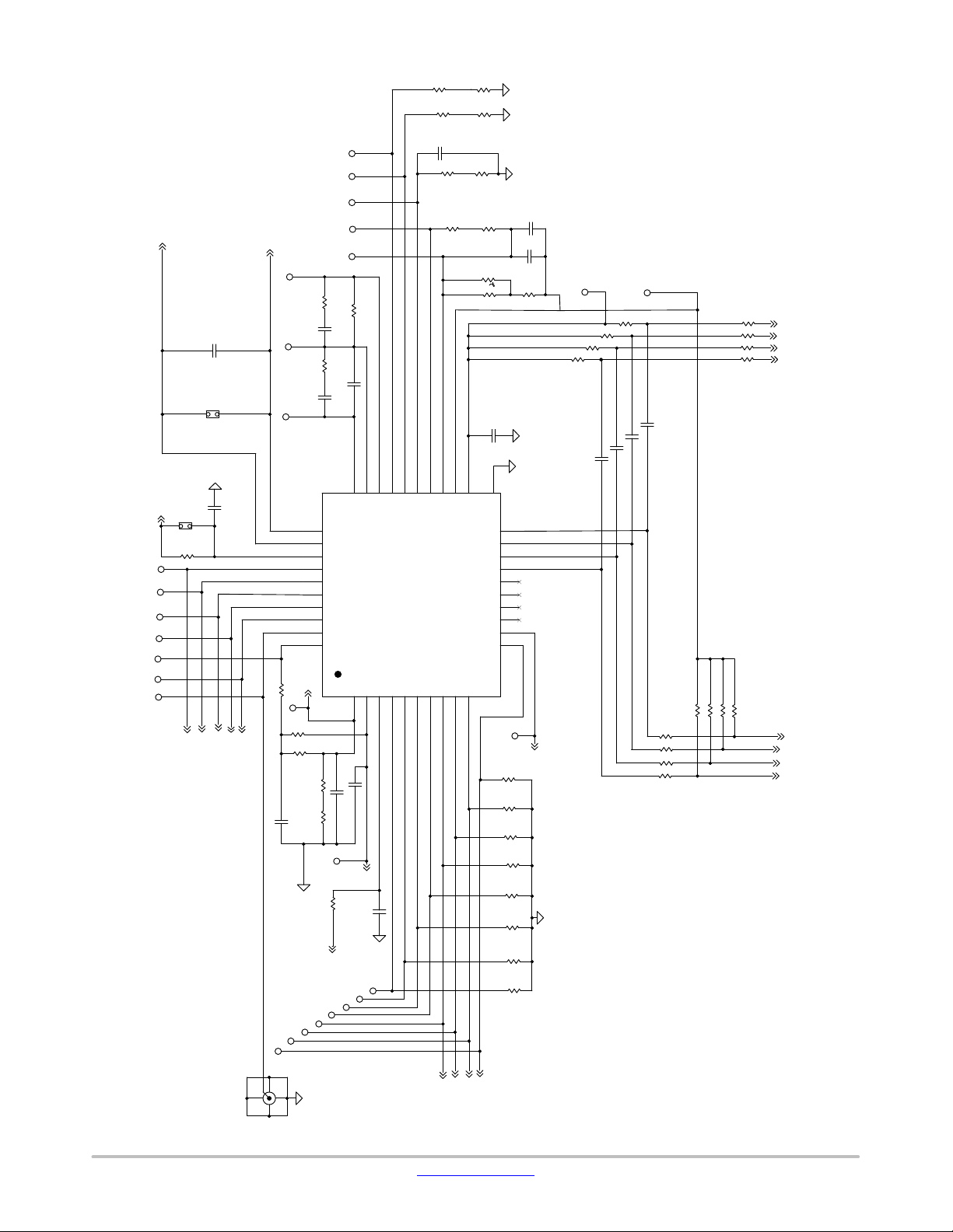
Figure 1. Typical Controller Application Circuit
www.onsemi.com
2
Page 3
NCP81276
C117
22uF
C112
22uF
C107
22uF
C102
VOUT
L1
0.22uH
22uF
C92
DNP
+
C82
DNP
+
CSNx
C72
330uF
+
C62
330uF
+
SWNx
R83
R82
SHORTPIN
SHORTPIN
1 2
1 2
VIN
C95
56uF
+
C85
10uF
C75
10uF
C65
10uF
C57
10uF
C52
10uF
C47
10uF
C39
10uF
0.1uF
TP64
C27
TP87
0.22uF
TP65
9
4
3
9
4
3
NCP81161U2
SW
G1G2S1
1
2108
SW
G1G2S1
1
8
7
HG
SW
PWM
BST
123
R60 0R
2108
C32
2.2R
R69
C37
R75
567
567
6
GND
EN
DNP
DNP
S2
Q6
S2
Q1
LGVCC
PAD
45
0R
0R
R59
R133
NTMFD4C85N
NTMFD4C85N
C22
4.7uF
TP63
DRON
PWMx
VCC_DRV
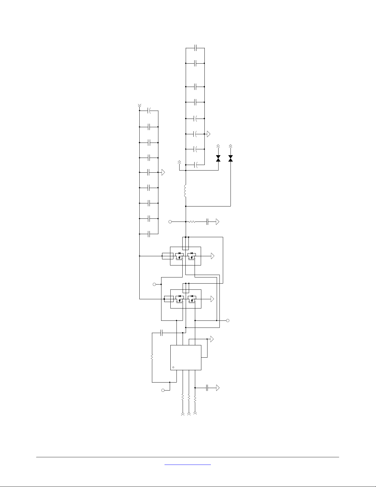
Figure 2. Typical Phase Application Circuit
www.onsemi.com
3
Page 4

NCP81276
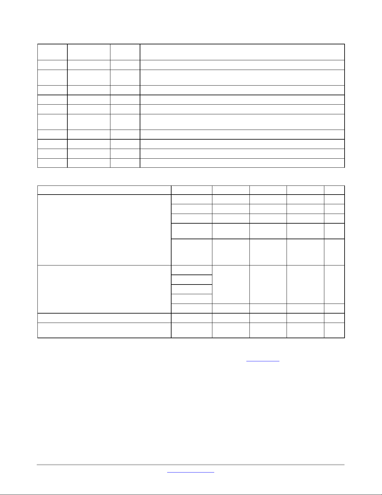
Table 1. PIN FUNCTION DESCRIPTION
Pin
Number
1 REFIN I Reference voltage input for output voltage regulation.
2 VREF O 2.0 V output reference voltage. A 10 nF ceramic capacitor is required to connect this pin
3 VRMP I Feed-forward input of VIN for the ramp slope compensation. The current fed into this pin
4 SS I/O Soft Start setting. During startup it is used to program the soft start time with a resistor to
5 OCP I/O Per OCP setting. During startup it is used to program the OCP level per phase and latch
6 LPC1 I/O Low phase count 1. During startup it is used to program the power zone (when PSI is set
7 LPC2 I/O Low phase count 2. During startup it is used to program boot-up power zone (when PSI
8 PWM4/PHTH1 I/O PWM 4 output/Phase Shedding Threshold 1. During startup it is used to program the
9 PWM3/PHTH2 I/O PWM 3 output/Phase Shedding Threshold 2. During startup it is used to program the
10 PWM2/PHTH3 I/O PWM 2 output/Phase Shedding Threshold 3. During startup it is used to program the
11 PWM1/PHTH4 I/O PWM 1 output/Phase Shedding Threshold 4. During startup it is used to program the
12 DRON I/O Bidirectional gate driver enable for external drivers.
13 NC N/A No connect pin. Please leave floating.
14 NC N/A No connect pin. Please leave floating.
15 NC N/A No connect pin. Please leave floating.
16 NC N/A No connect pin. Please leave floating.
17 CSP4 I Non-inverting input to current balance sense amplifier for phase 4. Pull-up to VCC to
18 CSP3 I Non-inverting input to current balance sense amplifier for phase 3. Pull-up to VCC to
19 CSP2 I Non-inverting input to current balance sense amplifier for phase 2. Pull-up to VCC to
20 CSP1 I Non-inverting input to current balance sense amplifier for phase 1. Pull-up to VCC to
21 CSREF I Total output current sense amplifier reference voltage input.
22 CSSUM I Inverting input of total current sense amplifier.
23 CSCOMP O Output of total current sense amplifier.
24 ILIM O Over current shutdown threshold setting output. The threshold is set by a resistor
25 IOUT O Total output current. A resistor to GND is required to provide a voltage drop of 2 V at the
26 LLTH/I2C_ADD I Load line selection from 0% to 100% and I2C address pin.
27 FSW I Resistor to ground form this pin sets the operating frequency of the regulator.
28 DIFF O Output of the regulators differential remote sense amplifier.
29 FB I Error amplifier inverting (feedback) input.
30 COMP O Output of the error amplifier and the inverting input of the PWM comparator.
31 VSP I Differential Output Voltage Sense Positive terminal.
Pin
Name
Pin
Type
Description
to ground.
is used to control of the ramp of PWM slope.
ground.
off time with a resistor to ground.
low) with a resistor to ground.
is set low) with a resistor to ground.
phase shedding threshold 1 (PSI set to mid state) with a resistor to ground.
phase shedding threshold 2 (PSI set to mid state) with a resistor to ground.
phase shedding threshold 3 (PSI set to mid state) with a resistor to ground.
phase shedding threshold 4 (PSI set to mid state) with a resistor to ground.
disable the PWM4 output.
disable the PWM3 output.
disable the PWM2 output.
disable the PWM1 output.
between ILIM and to CSCOMP pins.
maximum output current.
www.onsemi.com
4
Page 5
NCP81276
Table 1. PIN FUNCTION DESCRIPTION (continued)
Pin
Number
32 VSN I Differential Output Voltage Sense Negative terminal.
33 VCC I
34 SDA I/O Serial Data bi-directional pin, requires pull-up resistor to VCC.
35 SCL I Serial Bus clock signal, requires pull-up resistor to VCC.
36 EN I Logic input. Logic high enables regulator output logic low disables regulator output.
37 PSI I
38 PGOOD O Open Drain power good indicator.
39 PWM_VID I PWM_VID buffer input.
40 VID_BUFF O PWM_VID pulse output from internal buffer.
41 AGND GND Analog ground and thermal pad, connected to system ground.
Pin
Name
Table 2. MAXIMUM RATINGS
Rating
Pin Voltage Range (Note 1)
Pin Current Range
Moisture Sensitivity Level MSL 1 −
Lead Temperature Soldering Reflow (SMD Styles Only),
Pb-Free Versions (Note 2)
Stresses exceeding those listed in the Maximum Ratings table may damage the device. If any of these limits are exceeded, device functionality
should not be assumed, damage may occur and reliability may be affected.
1. All signals referenced to GND unless noted otherwise.
2. For information, please refer to our Soldering and Mounting Techniques Reference Manual, SOLDERRM/D
Pin
Type
Description
Power for the internal control circuits. A 1 mF decoupling capacitor is requires from this
pin to ground.
Power level control 3 level control. Use a current limiting resistor of 100 kW when driving
the pin with 5 V logic.
Pin Symbol Min Typ Max Unit
VSN GND−0.3 GND + 0.3 V
VCC −0.3 6.5 V
VRMP −0.3 25 V
PWM_VID −0.3
All Other Pins
with the
exception of
the DRON Pin
COMP
CSCOMP
DIFF
PGOOD
VSN −1 1 mA
T
SLD
(−2, < 50 ns)
−0.3 VCC + 0.3 V
−2 2 mA
260 °C
VCC + 0.3 V
.
www.onsemi.com
5
Page 6
NCP81276
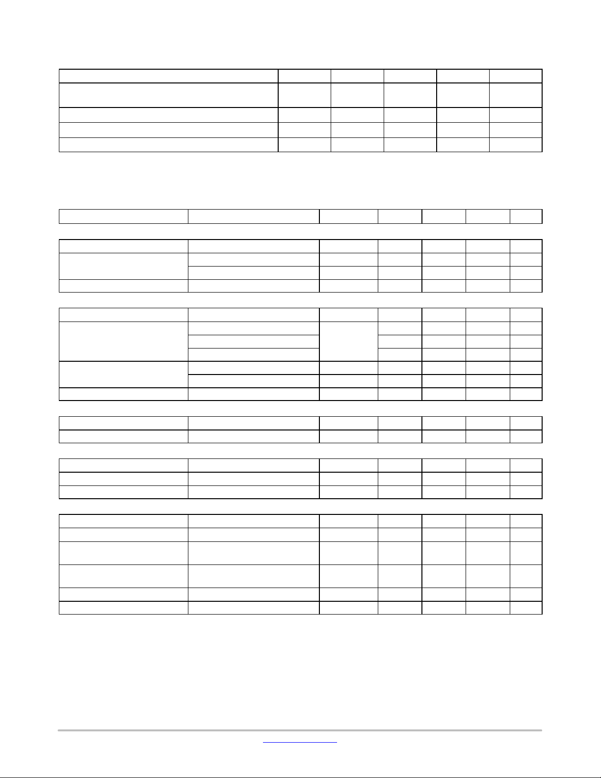
Table 3. THERMAL CHARACTERISTICS
Rating
Thermal Characteristics, (QFN40, 5 × 5 mm)
Thermal Resistance, Junction-to-Air (Note 1)
Operating Junction Temperature Range (Note 2) T
Operating Ambient Temperature Range T
Maximum Storage Temperature Range T
1. JESD 51−5 (1S2P Direct-Attach Method) with 0 LFM.
2. JESD 51−7 (1S2P Direct-Attach Method) with 0 LFM.
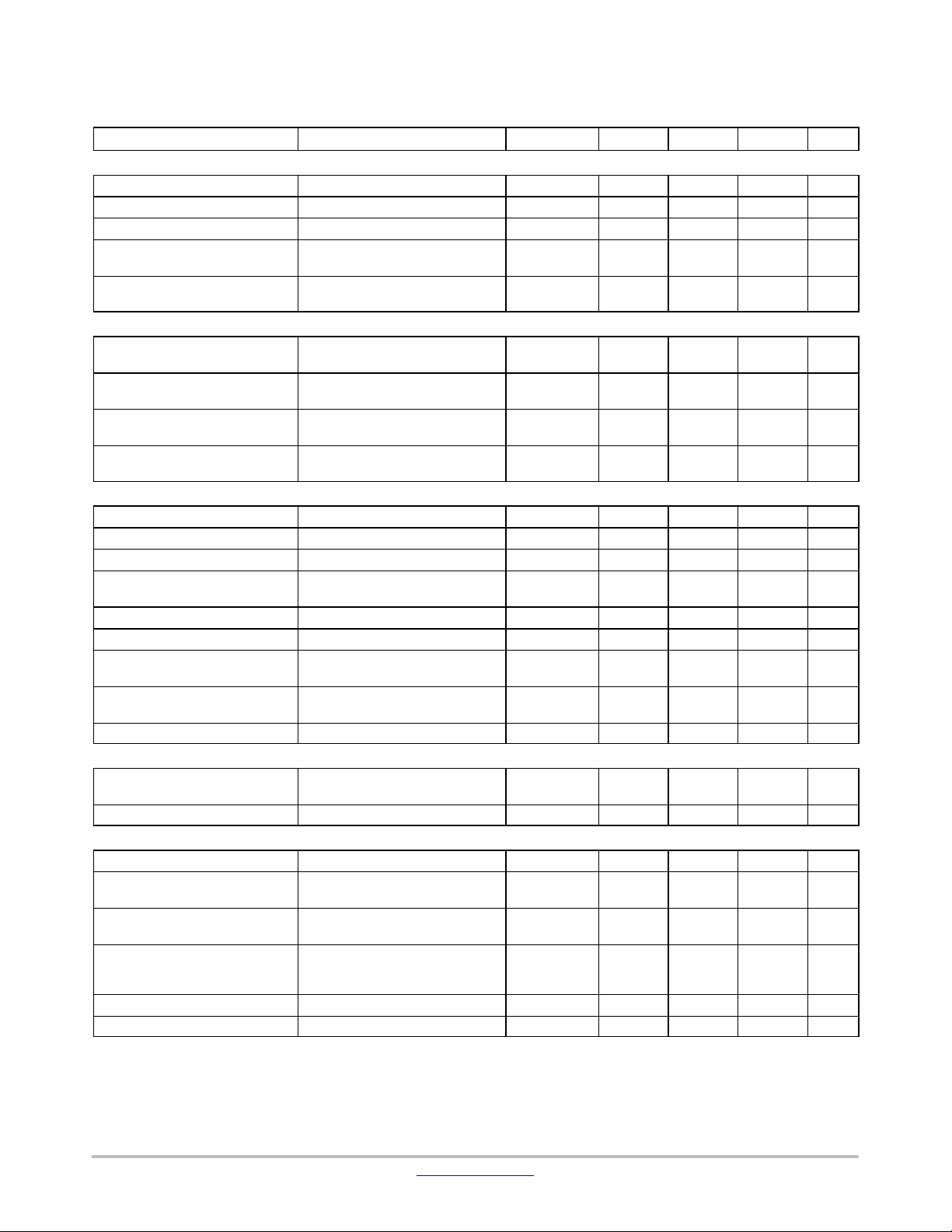
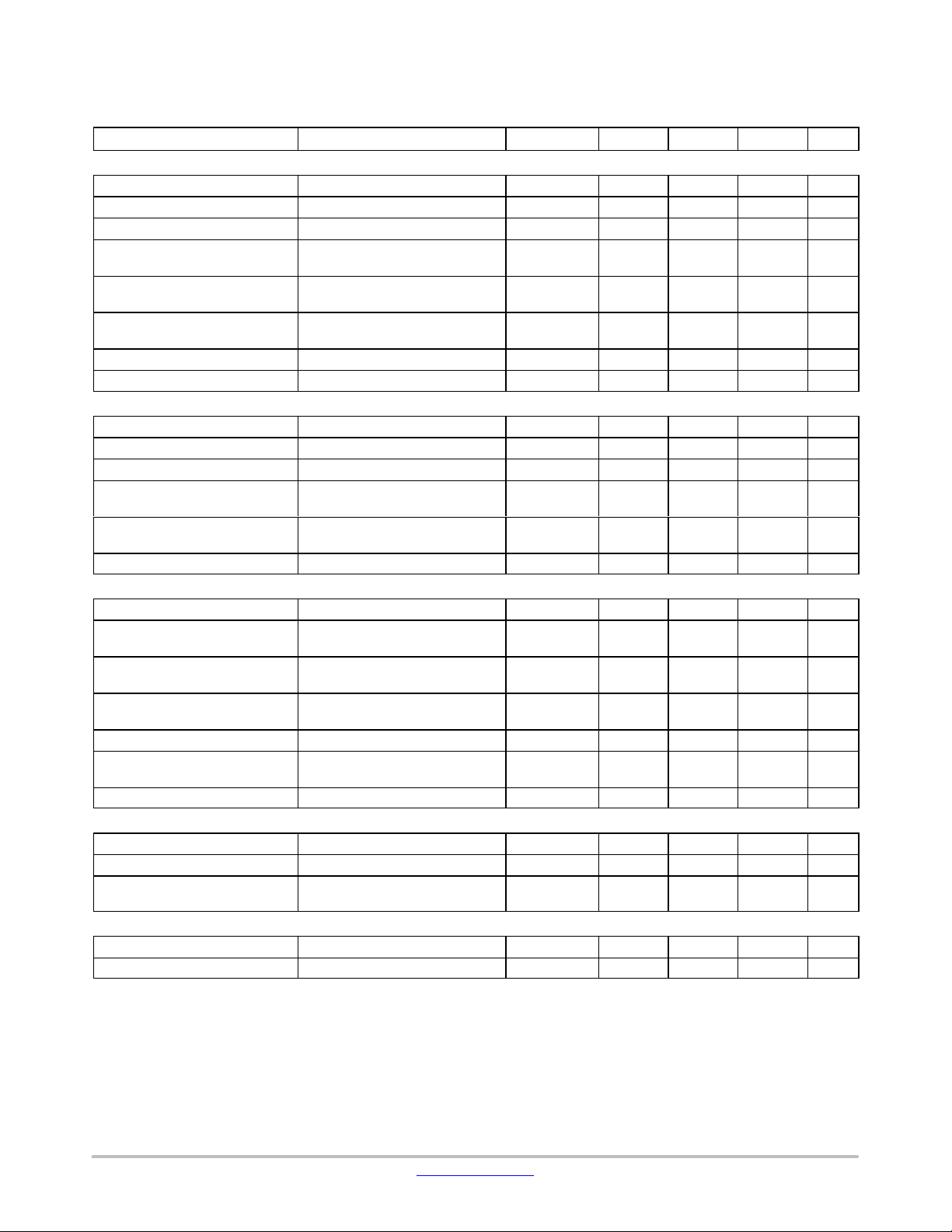
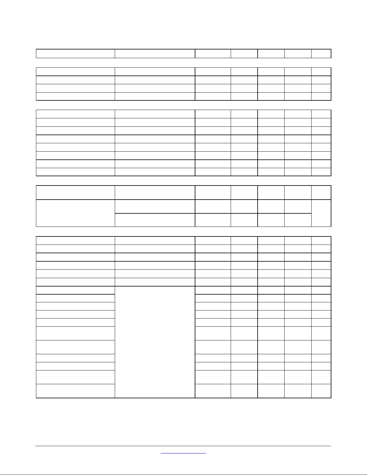
Table 4. ELECTRICAL CHARACTERISTICS
(Unless otherwise stated: −10°C < TA < 100°C; 4.6 V < VCC < 5.4 V; C
Parameter
VRMP
Supply Range
UVLO
VRMP Rising V
VRMP Falling V
VRMP UVLO Hysteresis V
BIAS SUPPLY
Supply Voltage Range
VCC Quiescent current
Enable Low
8 Phase Operation 50 mA
1 Phase-DCM Operation 10 mA
UVLO Threshold
VCC Rising UVLO
VCC Falling UVLO
VCC UVLO Hysteresis UVLO
SWITCHING FREQUENCY
Switching Frequency Range
8 Phase Configuration F
Switching Frequency Accuracy FSW = 810 kHz
ENABLE INPUT
Input Leakage
EN = 0 V or VCC I
Upper Threshold V
Lower Threshold V
DRON
Output High Voltage
Output Low Voltage
Rise Time
Sourcing 500 mA
Sinking 500 mA
Cl(PCB) = 20 pF,
DV
Fall Time
Cl(PCB) = 20 pF,
DV
Internal Pull-up Resistance R
Internal Pull-down Resistance VCC = 0 V R
Test Conditions Symbol Min Typ Max Unit
= 10% to 90%
O
= 10% to 90%
O
Symbol Min Typ Max Unit
R
θJA
J
A
STG
= 0.1 mF)
VCC
PULL−UP
PULL_DOWN
− 68 −
°C/W
−40 − 150
−10 − 100
−55 − 150
_C
_C
_C
VRMP 4.5 20 V
RMPrise
RMPfall
RMPhyst
3 V
800 mV
4.2 V
VCC 4.6 5.4 V
40
4.5 V
mA
0.6 V
0.1 V
kW
kW
DF
V
ICC
OH
V
OL
t
t
SW
L
IH
IL
R
F
SW
Rise
Fall
Hyst
4 V
200 mV
250 1200 kHz
−4 +4 %
−1.0 1.0
1.2 V
3.0 V
160 ns
3 ns
2.0
70
mA
www.onsemi.com
6
Page 7
NCP81276
Table 4. ELECTRICAL CHARACTERISTICS (continued)
(Unless otherwise stated: −10°C < TA < 100°C; 4.6 V < VCC < 5.4 V; C
Parameter UnitMaxTypMinSymbolTest Conditions
PGOOD
I
Output Low Voltage
Leakage Current P
= 10 mA (Sink) V
PGOOD
= 5 V I
GOOD
Output Voltage Initialization Time T_init 1.5 ms
Minimum Output Voltage Ramp
Time
Maximum Output Voltage Ramp
Time
PROTECTION-OCP, OVP, UVP
Under Voltage Protection (UVP)
Relative to REFIN Voltage UVP 300 mV
Threshold
Under Voltage Protection (UVP)
Delay
Over Voltage Protection (OVP)
Relative to REFIN Voltage OVP 400 mV
Threshold
Over Voltage Protection (OVP)
Delay
PWM OUTPUTS
Output High Voltage
Sourcing 500 mA
Output Mid Voltage V
Output Low Voltage
Rise and Fall Time
Sinking 500 mA
CL(PCB) = 50 pF, DVO = 10% to
90% of VCC
Tri-state Output Leakage Gx = 2.0 V, x = 1−8, EN = Low I
Minimum On Time FSW = 600 kHz Ton 12 ns
0% Duty Cycle Comp Voltage when PWM Outputs
Remain LOW
100% Duty Cycle Comp Voltage when PWM Outputs
Remain HIGH
PWM Phase Angle Error Between Adjacent Phases ø ±15 °
PHASE DETECTION
Phase Detection Threshold
CSP2 to CSP8 V
Voltage
Phase Detect Timer CSP2 to CSP8 T
ERROR AMPLIFIER
Input Bias Current
Open Loop DC Gain CL = 20 pF to GND,
= 10 kW to GND
R
L
Open Loop Unity Gain Bandwidth CL = 20 pF to GND,
= 10 kW to GND
R
L
Slew Rate
Maximum Output Voltage I
Minimum Output Voltage I
DVIN = 100 mV, G = −10 V/V,
= 0.75–1.52 V, CL = 20 pF
DV
OUT
to GND, R
SOURCE
SINK
= 10 kW to GND
L
= 2 mA V
= 2 mA V
VCC
= 0.1 mF)
OL
T_ramp
T_ramp
T
UVP
T
OVP
V
OH
MID
V
OL
tR, t
VCOMP
VCOMP
PHDET
PHDET
I
BIAS
G
L
L
OL
MIN
MAX
0.15 ms
10 ms
5
5
VCC − 0.2 V
1.9 2.0 2.1 V
F
10 ns
−1.0 1.0
0%
100%
1.3 V
2.5 V
1.1 ms
−400 400 nA
80 dB
0.4 V
0.2
0.7 V
VCC − 0.1 V
GBW 20 MHz
SR 5
OUT
OUT
3.5 V
1 V
V/ms
mA
ms
ms
mA
www.onsemi.com
7
Page 8
NCP81276
Table 4. ELECTRICAL CHARACTERISTICS (continued)
(Unless otherwise stated: −10°C < TA < 100°C; 4.6 V < VCC < 5.4 V; C
Parameter UnitMaxTypMinSymbolTest Conditions
DIFFERENTIAL SUMMING AMPLIFIER
Input Bias Current
VSP Input Voltage V
VSN Input Voltage V
−3dB Bandwidth CL = 20 pF to GND,
= 10 kW to GND
R
L
Closed Loop DC Gain
VSP to VSN = 0.5 to 1.3 V G 1 V/V
(VSP−VSN to DIFF)
Droop accuracy CSREF − DROOP = 80 mV,
V
= 0.8 V to 1.2 V
REFIN
Maximum Output Voltage I
Minimum Output Voltage I
= 2 mA V
SOURCE
= 2 mA V
SINK
CURRENT SUMMING AMPLIFIER
Offset Voltage
Input Bias Current CSSUM = CSREF = 1 V I
Open Loop Gain G 80 dB
Current sense Unity Gain
Bandwidth
Maximum CSCOMP Output
Voltage
Minimum CSCOMP Output Voltage I
CL = 20 pF to GND,
= 10 kW to GND
R
L
I
= 2 mA V
SOURCE
= 2 mA V
SINK
CURRENT BALANCE AMPLIFIER
Input Bias Current
Common Mode Input Voltage
CSPX − CSP
CSPX = CSREF V
= 1.2 V I
X+1
Range
Differential Mode Input Voltage
CSREF = 1.2 V V
Range
Closed Loop Input Offset Voltage
Matching
CSPX = 1.2 V, Measured from the
Average
Current Sense Amplifier Gain 0 V < CSPX < 0.1 V G 5.7 6.0 V/V
Multiphase Current Sense Gain
CSREF = CSP = 10 mV to 30 mV
Matching
−3dB Bandwidth BW 8 MHz
IOUT
Input Reference Offset Voltage
Output Current Max
Current Gain
ILIM to CSREF V
ILIM Sink Current 20 mA
IOUT/ILIM, R
= 5 kW
R
IOUT
= 20 kW,
LIM
VOLTAGE REFERENCE
I
VREF Reference Voltage
VREF Reference accuracy T
= 1 mA VREF 1.98 2 2.02 V
REF
< TJ < T
JMIN
JMAX
VCC
= 0.1 mF)
I
BIAS
IN
IN
−400 400 nA
0 2 V
−0.3 0.3 V
BW 12 MHz
DDROOP
OUT
OUT
V
OS
L
78 82 mV
3 V
0.8 V
−500 500
−7.5 7.5
GBW 10 MHz
OUT
OUT
BIAS
CM
DIFF
3.5 V
0.1 V
−50 50 nA
0 2 V
−100 100 mV
−1.5 1.5 mV
DG
I
OUT
OS
−3 3 %
−3 +3 mV
200
G 9.5 10 10.5 A/A
DVREF
1 %
mV
mA
mA
www.onsemi.com
8
Page 9
NCP81276
Table 4. ELECTRICAL CHARACTERISTICS (continued)
(Unless otherwise stated: −10°C < TA < 100°C; 4.6 V < VCC < 5.4 V; C
Parameter UnitMaxTypMinSymbolTest Conditions
PSI
PSI High Threshold
PSI Mid threshold V
PSI Low threshold V
PSI Input Leakage Current V
= 0 V I
PSI
PWM_VID BUFFER
Upper Threshold
Lower Threshold V
PWM_VID Switching Frequency F
Output Rise Time t
Output Fall Time t
Rising and Falling Edge Delay
Propagation Delay tPD = t
Propagation Delay Error
Dt = tR − t
PDHL
DtPD = t
F
PDHL
= t
− t
PDLH
PDLH
REFIN
REFIN Discharge Switch
ON-Resistance
Ratio of Output Voltage Ripple
Transferred from REFIN/REFIN
Voltage Ripple
I
REEFIN(SINK)
F
PWM_VID
F
≤ 600 kHz
SW
F
PWM_VID
F
≤ 600 kHz
SW
= 2 mA R
= 400 kHz,
= 1000 kHz,
I2C
Logic High Input Voltage
Logic Low Input Voltage V
Hysteresis (Note 4) 80 mV
Output Low Voltage I
= −6 mA V
SDA
Input Current I
Input Capacitance (Note 4) C
Clock Frequency
See Figure 3
SCL Low Period (Note 4) t
SCL High Period (Note 4) t
SCL/SDA Rise Time (Note 4) t
SCL/SDA Fall Time (Note 4) t
Start Condition Setup Time
(Note 4)
Start Condition Hold Time
(Note 1, 4)
Data Setup Time (Note 2, 4) t
Data Hold Time (Note 2, 4) t
Stop Condition Setup Time
(Note 3, 4)
Bus Free Time between Stop
and Start (Note 4)
Product parametric performance is indicated in the Electrical Characteristics for the listed test conditions, unless otherwise noted. Product
performance may not be indicated by the Electrical Characteristics if operated under different conditions.
1. Time from 10% of SDA to 90% of SCL.
2. Time from 10% or 90%of SDA to 10% of SCL.
3. Time from 90% of SCL to 10% of SDA.
4. Guaranteed by design, not production tested.
VCC
= 0.1 mF)
V
MID
V
PWM_VID
Dt
t
PD
Dt
DISCH
V
ORP/VREFIN
V
ORP/VREFIN
V
SDA
f
SCL
LOW
HIGH
t
SU;STA
t
HD;STA
SU;DAT
HD;DAT
t
SU;STO
t
BUF
IH
L
IH
R
F
PD
IH
IL
OL
L
, C
R
F
1.45 V
0.8 1 V
IL
−1 1
0.575 V
mA
1.21 V
IL
0.575 V
400 5000 kHz
3 ns
3 ns
0.5 ns
8 ns
0.5 ns
10
10
W
%
30
1.7 V
0.5 V
0.4 V
SCL
−1 1
5 pF
mA
400 kHz
1.3
0.6
ms
ms
300 ns
300 ns
600 ns
600 ns
100 ns
300 ns
600 ns
1.3
ms
www.onsemi.com
9
Page 10
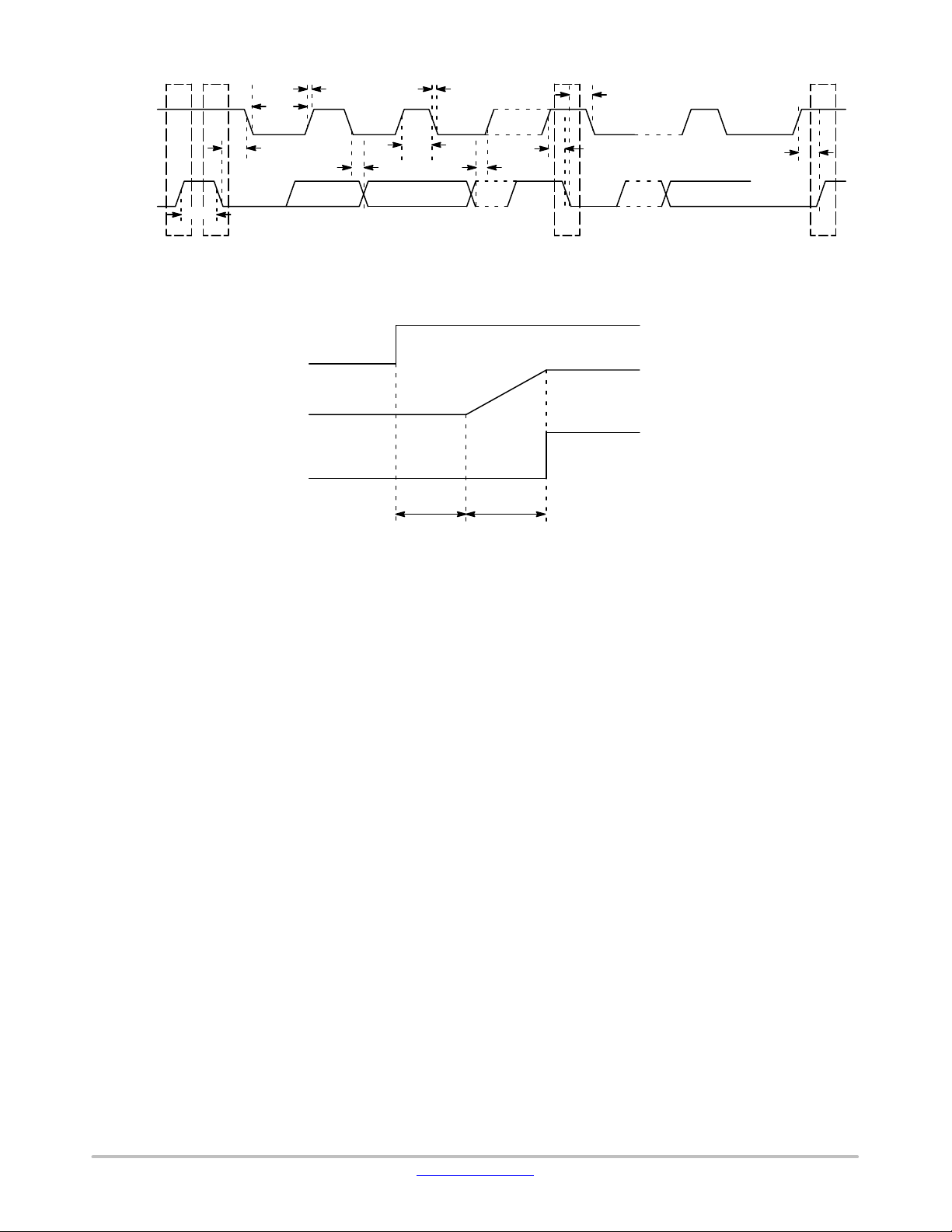
NCP81276
SCLK
SDATA
t
t
HD:DAT
R
t
HIGH
t
LOW
t
HD:STA
t
BUF
STOP START START STOP
t
SU:DAT
t
F
t
SU:STA
t
HD:STA
t
SU:STO
Figure 3. I2C Timing Diagram
EN
VOUT
PGOOD
T_init
T_ramp
Figure 4. Soft Start Timing Diagram
Applications Information
The NCP81276 is a buck converter controller optimized
for the next generation computing and graphic processor
applications. It contains four PWM channels which can be
individually configured to accommodate buck converter
configurations up to four phases. The controller regulates
the output voltage all the way down to 0 V with no load.
Also, the device is functional with input voltages as low as
3.3 V.
The output voltage is set by applying a PWM signal to the
PWM_VID input of the device. The controller converts the
PWM_VID signal with variable high and low levels into
a constant amplitude PWM signal which is then applied to
the REFIN pin. The device calculates the average value of
this PWM signal and sets the regulated voltage accordingly .
The output voltage is differentially sensed and subtracted
from the REFIN average value. The result is biased up to
1.3 V and applied to the error amplifier. Any difference
between the sensed voltage and the REFIN pin average
voltage will change the PWM outputs duty cycle until the
two voltages are identical. The load current is current is
continuously monitored on each phase and the PWM
outputs are adjusted to ensure adjusted to ensure even
distribution of the load current across all phases. In addition,
the total load current is internally measured and used to
implement a programmable adaptive voltage positioning
mechanism.
The device incorporates overcurrent, under and
overvoltage protections against system faults.
The communication between the NCP81276 and the user
is handled with two interfaces, PWM_VID to set the output
voltage and I
2
C to configure or monitor the status of the
controller. The operation of the internal blocks of the device
is described in more details in the following sections.
www.onsemi.com
10
Page 11
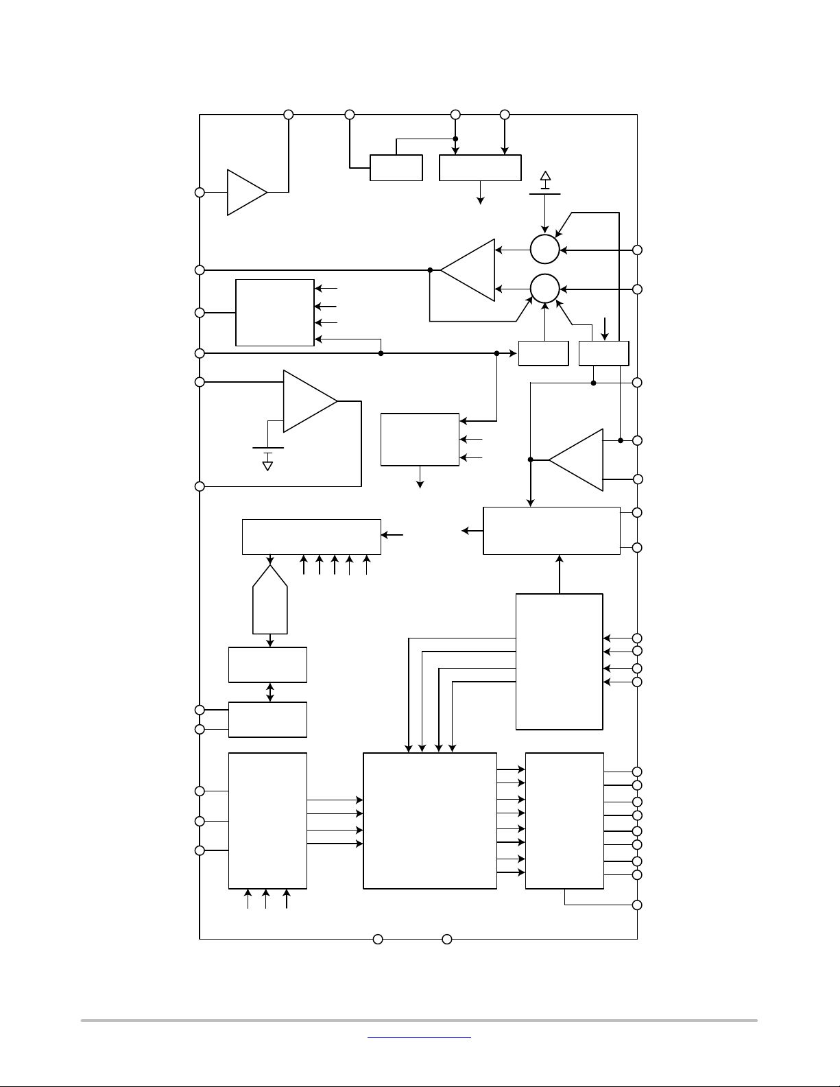
NCP81276
VID_BUFF VREF VCC EN
REF UVLO & EN
PWM_VID
DIFFOUT
PGOOD
REFIN
FB
COMP
PGOOD
Comparator
−
1.3V
+
Mux
EN
VSP
VSN
OVP
OVP
PSI
OCP
1.3V
EN
+
−
VSP
VSN
Measurment , ILIM & OCP
S
S
Soft start
Total Output Current
LLTH
LLTH
+
−
VSP
VSN
CSCOMP
CSREF
CSSUM
ILIM
IOUT
SDA
SCL
FSW
VRMP
PSI
FSW
CSP1 to CSP4
LLTH/I2C_ADD
PWM
Generators
GND LLTH/I2C_ADD
ADC
Data
Registers
Control
Interface
Ramp
Generators
OVP
OCP
IOUT
PWM1 to PWM4
Ramp1
Ramp2
Ramp3
Ramp4
EN
Figure 5. NCP81276 Functional Block Diagram
IPH1
IPH2
IPH3
IPH4
Current Balance
Amplifiers
and
per Phase OCP
Comparators
Power State
Stage
CSP1
CSP2
CSP3
CSP4
PWM1/PHTH4
PWM2/PHTH3
PWM3/PHTH2
PWM4/PHTH1
LPC2
LPC1
OCP
SS
DRON
www.onsemi.com
11
Page 12
NCP81276
VCC
F
PWM_VID Interface
PWM_VID is a single wire dynamic voltage control
interface where the regulated voltage is set by the duty cycle
of the PWM signal applied to the controller.
The device controller converts the variable amplitude
PWM signal into a constant 2 V amplitude PWM signal
while preserving the duty cycle information of the input
signal. In addition, if the PWM_VID input is left floating,
the VID_BUFF output is tri-stated (floating).
The constant amplitude PWM signal is then connected to
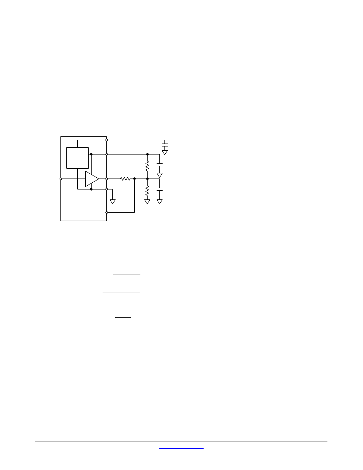
the REFIN pin through a scaling and filtering network (see
Figure 6). This network allows the user to set the minimum
and maximum REFIN voltages corresponding to 0% and
100% duty cycle values.
R1
R2
0.1 mF
10n
C1
PWM_VID
Internal
precision
reference
= 2 V
V
REF
Controller
VREF
VID_BUFF
R3
GND
REFIN
Figure 6. PWM_VID Interface
The minimum (0% duty cycle), maximum (100% duty
cycle) and boot (PWM_VID input floating) voltages can be
calculated with the following formulas:
1 )
1 )
REF
1
R
1@R3
ǒ
R1)R
R2)R
1
R
1
R
2
Ǔ
3
Ǔ
3
3
R
@
2
1
ǒ
R
@
1
R2@R
@
1 )
(eq. 1)
(eq. 2)
(eq. 3)
Soft Start
V
V
MAX
MIN
V
+ V
+ V
BOOT
REF
REF
@
@
+ V
Soft start is defined as the transition from Enable assertion
high to the assertion of Power good as shown in Figure 4.
The output is set to the desired voltage in two steps, a fixed
initialization step of 1.5 ms followed by a ramp-up step
where the output voltage is ramped to the final value set by
the PWM_VID interface. During the soft start phase,
PGOOD pin is initially set low and will be set high when the
output voltage is within regulation and the soft start ramp is
complete. The PGOOD signal only de-asserts (pull low)
when the controller shuts down due to a fault condition
(UVLO, OVP or OCP event).
The output voltage ramp-up time is user settable by
connecting a resistor between pin SS and GND. The
controller will measure the resistance value at power-up by
sourcing a 10 mA current through this resistor and set the
ramp time (t
Remote Voltage Sense
) as shown in Table 16.
ramp
A high performance true differential amplifier allows the
controller to measure the output voltage directly at the load
using the VSP (VOUT) and VSN (GND) pins. This keeps
the ground potential differences between the local controller
ground and the load ground reference point from affecting
regulation of the load. The output voltage of the differential
amplifier is set by the following equation:
V
DIFOUT
ǒ
+
V
* V
VSP
ǒ
V
DROOP
) V
)
VSN
Ǔ
)
CSREF
ǒ
1.3 V * V
Ǔ
REFIN
Ǔ
)
(eq. 4)
Where:
V
DIFOUT
V
VSP
is the output voltage of the differential amplifier.
− V
is the regulated output voltage sensed at the
VSN
load.
V
is the voltage at the output pin set by the
REFIN
PWM_VID interface.
V
DROOP
− V
is the expected drop in the regulated
CSREF
voltage as a function of the load current (load-line).
1.3 V is an internal reference voltage used to bias the
amplifier inputs to allow both positive and negative
output voltage for V
Error Amplifier
DIFOUT
.
A high performance wide bandwidth error amplifier is
provided for fast response to transient load events. Its
inverting input is biased internally with the same 1.3 V
reference voltage as the one used by the differential sense
amplifier to ensure that both positive and negative error
voltages are correctly handled.
An external compensation circuit should be used (usually
type III) to ensure that the control loop is stable and has
adequate response.
Ramp Feed-Forward Circuit
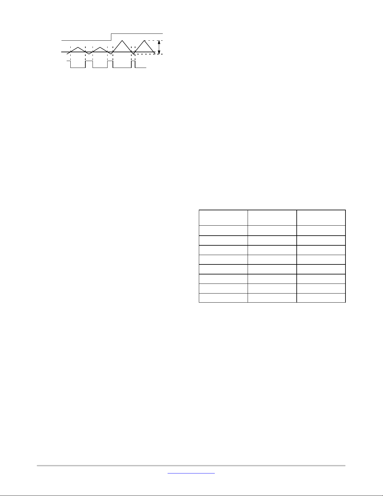
The ramp generator circuit provides the ramp used to
generate the PWM signals using internal comparators (see
Figure 7) The ramp generator provides voltage
feed-forward control by varying the ramp magnitude with
respect to the VRMP pin voltage. The PWM ramp time is
changed according to the following equation:
V
RAMPpk+pk
+ 0.1 @ V
pp
VRMP
(eq. 5)
The VRMP pin also has a UVLO function. The VRMP
UVLO is only active after the controller is enabled. The
VRMP pin is high impedance input when the controller is
disabled.
www.onsemi.com
12
Page 13
NCP81276
p
V
IN
V
Comp-IL
Duty
Figure 7. Ramp Feed-Forward Circuit
PWM Output Configuration
ramp_p
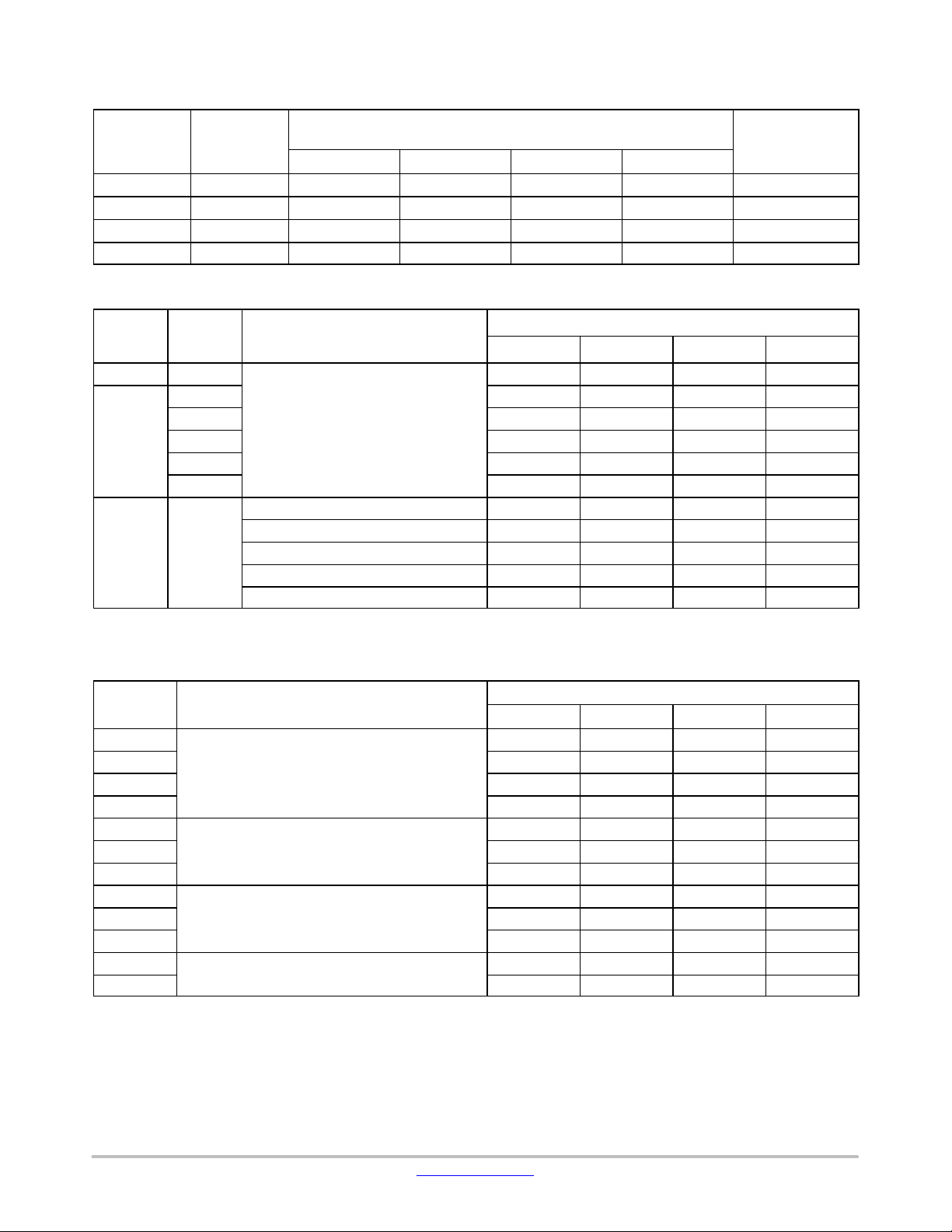
By default the controller operates in 4 phase mode,
however with the use of the CSP pins the phases can be
disabled by connecting the CSP pin to VCC. At power-up
the NCP81276 measures the voltage present at each CSP pin
and compares it with the phase detection threshold. If the
voltage exceeds the threshold, the phase is disabled. The
phase configurations that can be achieved by the device are
listed in Table 6. The active phase (PWM
) information is
X
also available to the user in the phase status register.
PSI, LPCX, PHTH
X
The NCP81276 incorporates a power saving interface
(PSI) to maximize the efficiency of the regulator under
various loading conditions. The device supports up to six
distinct operation modes, called power zones using the PSI,
LPC
and PHTHX pins (see Table 7). At power-up the
X
controller reads the PSI pin logic state and sources a 10 mA
current through the resistors connected to the LPC
PHTH
pins, measures the voltage at these pins and
X
X
and
configures the device accordingly.
The configuration can be changed by the user by writing
to the LPC
and PHTHX configuration registers.
X
After EN is set high, the NCP81276 ignores any change
in the PSI pin logic state until the output voltage reaches the
nominal regulated voltage.
When PSI = High, the controller operates with all active
phases enabled regardless of the load current. If PSI = Mid,
the NCP81276 operates in dynamic phase shedding mode
where the voltage present at the IOUT pin (the total load
current) is measured every 10 ms and compared to the
PHTH
thresholds to determine the appropriate power
X
zone.
The resistors connected between the PHTH
and GND
X
should be picked to ensure that a 10 mA current will match
the voltage drop at the IOUT pin at the desired load current.
Please note that the maximum allowable voltage at the
IOUT pin at the maximum load current is 2 V. Any PHTH
threshold can be disabled if the voltage drop across the
PHTH
resistor is ≥ 2 V for a 10 mA current, the pin is left
X
floating or 0xFF is written to the appropriate PHTH
configuration register.
At power-up, the automatic phase shedding mode is only
enabled after the output voltage reaches the nominal
regulated voltage.
When PSI = Low, the controller is set to a fixed power
zone regardless of the load current. The LPC2 setting
controls the power zone used during boot-up (after EN is set
high) while the LPC1 configuration sets the power zone
during normal operation. If PSI = Low during power-up, the
configuration set by LPC1 is activated only after PSI leaves
the low state (set to Mid or High) and set again to the low
state.
LLTH/I2C_ADD
The LLTH/I2C_ADD pin enables the user to change the
percentage of the externally programmed droop that takes
effect on the output. In addition, the LLTH/I2C_ADD pin
sets the I
2
C slave address of the NCP81276. The maximum
load line is controlled externally by setting the gain of the
current sense amplifier. On power up a 10 mA current is
sourced from the LLTH/I2C_ADD pin through a resistor
and the resulting voltage is measured. The load line and I
slave address configurations achievable using the external
resistor is listed in the table below. The percentage load line
can be fine-tuned over the I
2
C interface by writing to the LL
configuration register.
Table 5. LLTH/I2C_ADD PIN SETTING
Resistor
(kW)
10
23.2 0 0x20
37.4 100 0x30
54.9 0 0x30
78.7 100 0x40
110 0 0x40
147 100 0x50
249 0 0x50
NOTE: 1% tolerance.
X
X
Load Line
(%)
100 0x20
Slave Address
(Hex)
2
C
www.onsemi.com
13
Page 14
NCP81276
Table 6. PWM OUTPUT CONFIGURATION
(3 = Normal Connection, X = Tied to VCC)
Configuration
1 4 Phase
2 3 Phase
3 2 Phase
4 1 Phase
Phase
Configuration
CSP1 CSP2 CSP3 CSP4
3 3 3 3
3 3 3
3 3
3
Table 7. PSI, LPCX, PHTHX CONFIGURATION (Note 1)
PSI
Logic
State
High Disabled
Low
Mid Function
1. 1% tolerance.
2. Power zone 4 is DCM @100 kHz switching frequency, while zones 0 to 3 are CCM.
LPC
X
Resistor
(kW)
10 0 0 0 0
23.2 0 0 0 0
37.4 2 0 0 0
54.9 3 3 3 0
78.7 4 4 4 4
Disabled
IOUT vs. PHTHX Comparison
Function Disabled
IOUT > PHTH4 0 0 0 0
PTHT4 > IOUT > PHTH3 0 0 0 0
PHTH3 > IOUT > PHTH2 2 0 0 0
PHTH2 > IOUT > PHTH1 3 3 3 0
IOUT < PHTH1 4 4 4 4
CSP Pin Configuration
X X X 1
4 Phase 3 Phase 2 Phase 1 Phase
0 0 0 0
Enabled
PWM Outputs
(PWM
X
1, 2, 3, 4
X 1, 2, 3
X X 1, 2
Power Zone (Note 2)
Pins)
Table 8. PHASE SHEDDING CONFIGURATIONS
Power Zone PWM Output Configuration
0
2
3
4
0
3
4
0
3
4
0
4
4 Phase
3 Phase
2 Phase
1 Phase
PWM Output Status (3 = Enabled, X = Disabled)
PWM1 PWM2 PWM3 PWM4
3 3 3 3
3
3
3
3 3 3
3
3
3 3
3
3
3
3
X
X X X
X X X
X X X
X X X
X X X
X X X
X X X
X X X
3
X X
X
X
www.onsemi.com
14
Page 15
NCP81276
S
N
Power Zone Transition/Phase Shedding
The power zones supported by the NCP81276 are set by
the resistors connected to the LPC
PHTH
pins (PSI = Mid).
X
pins (PSI = Low) or
X
When PSI is set to the Mid-state, the NCP81276 employs
a phase shedding scheme where the power zone is
automatically adjusted for optimal efficiency by
continuously measuring the total output current (voltage at
the IOUT pin) and compare it with the PHTH
thresholds.
X
When the comparison result indicates that a lower power
zone number is required (an increase in the IOUT value), the
controller jumps to the required power zone immediately.
A decrease in IOUT that indicates that the controller needs
to switch into a higher power zone number, the transition
will be executed with a delay of 200 ms set by the phase shed
delay configuration register. The value of the delay can be
adjusted by the user in steps of 10 ms if required. To avoid
excessive ripple on the output voltage, all power zone
changes are gradual and include all intermediate power
zones between the current zone and the target zone set by the
comparison of the output current with the PHTH
thresholds, each transition introducing a programmable
200 ms delay. To avoid false changes from one power zone
to another caused by noise or short IOUT transients, the
comparison between IOUT and PHTH
threshold uses
X
Total Current Sense Amplifier
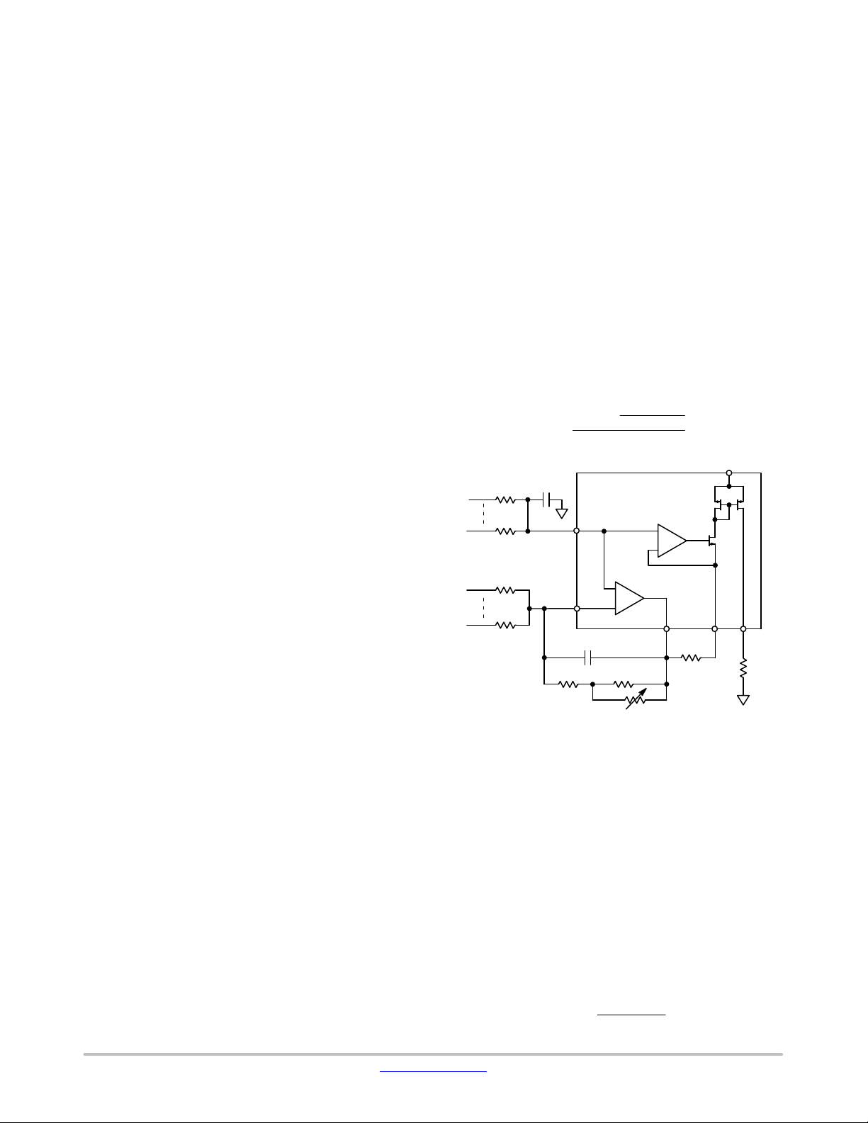
The controller uses a patented approach to sum the phase
currents into a single temperature compensated total current
signal (Figure 8).
This signal is then used to generate the output voltage
droop, total current limit, and the output current monitoring
functions. The total current signal is floating with respect to
CSREF. The current signal is the difference between
CSCOMP and CSREF. The REF(n) resistors sum the signals
from the output side of the inductors to create a low
impedance virtual ground.
The amplifier actively filters and gains up the voltage
applied across the inductors to recover the voltage drop
across the inductor series resistance (DCR). RTH is placed
near an inductor to sense the temperature of the inductor.
This allows the filter time constant and gain to be a function
of the NTC’s resistance (RTH) and compensate for the
change in the DCR with temperature.
The DC gain equation for the current sensing:
X
V
CSCOMP*CSREF
RREF1
CSN1
RCS2 )
+*
CREF
RCS1@RTH
RCS1)RTH
RPH
Controller
@ I
OUT
Total
VCC
1:10
(eq. 6)
@ DCR
hysteresis. The switch to a lower power zone is executed if
IOUT exceeds the PHTH
a transition to a higher power zone number is only executed
if IOUT is below PHTH
value is set to 0x10h and can be changed by the user by
writing to the phase shedding configuration register. If
a power zone/PHTHX threshold is disabled, the controller
will skip it during the power zone transition process.
When PSI = Low and the user requires to change the
power zone, the transition to the new power zone is identical
to the transition process used when PSI is set to the
threshold values while
X
-Hysteresis value. The hysteresis
X
CSN8
WN1
SWN8
RREF8
RPH1
RPH8
CSREF
CSSUM
RCS2
CCS
+
−
CSCOMP
RCS1
+
−
ILIM
RILIM
IOUT
RIMO
Mid-state. The only exception is when the target power zone
is disabled in automatic phase shedding mode. In this case,
the controller will automatically enable the target power
zone and allow the transition. When the controller is set to
automatic phase shedding, the power zone will be
automatically disabled.
Switching Frequency
A programmable precision oscillator is provided. The
clock oscillator serves as the master clock to the ramp
generator circuit. This oscillator is programmed by a resistor
to ground on the FSW pin. The FSW pin provides
approximately 2 V out and the source current is mirrored
into the internal ramp oscillator. The oscillator frequency is
approximately proportional to the current flowing in the
resistor. Table 19 lists the switching frequencies that can be
set using discrete resistor values for each phase
configuration. Also, the switching frequency information is
available in the FSW configuration register and it can be
changed by the user by writing to the FSW configuration
register.
www.onsemi.com
15
Figure 8. Total Current Summing Amplifier
Set the gain by adjusting the value of the RPH resistors.
The DC gain should be set to the output voltage droop. If the
voltage from CSCOMP to CSREF is less than 100 mV at the
maximum output current IOUT
increasing the gain of the CSCOMP amp. This is required to
provide a good current signal to offset voltage ratio for the
ILIMIT pin. The NTC should be placed near the inductor
used by phase 1. The output voltage droop should be set with
the droop filter divider.
The pole frequency in the CSCOMP filter should be set
equal to the zero from the output inductor. This allows the
circuit to recover the inductor DCR voltage drop current
signal. It is best to fine tune this filter during transient
testing.
F
+
Z
RTH
MAX
DCR@25C
2 @ p @ L
then it is recommend
(eq. 7)
Phase
Page 16
NCP81276
Programming the Current Limit ILIM
The current limit thresholds are programmed with
a resistor between the ILIMIT and CSCOMP pins. The
ILIMIT pin mirrors the voltage at the CSREF pin and
mirrors the sink current internally to IOUT (reduced by the
IOUT Current Gain) and the current limit comparators. The
100% current limit trips if the ILIMIT sink current exceeds
10 mA for 50 ms. The 150% current limit trips with minimal
delay if the ILIMIT sink current exceeds 15 mA. Set the
value of the current limit resistor based on the
CSCOMP−CSREF voltage as shown below.
V
RILIM +
CSCOMP*CSREF@ILIMIT
10 mA
(eq. 8)
or
RCS2)
RILIM +
Programming DROOP
RCS1@RTH
RCS1)RTH
RPH
10 mA
@ I
OUT
LIMIT
@ DCR
(eq. 9)
The signals CSCOMP and CSREF are differentially
summed with the output voltage feedback to add precision
voltage droop to the output voltage.
ǒ
Droop + DCR @
RCS1 ø RTHǓ) RCS2
RPH
(eq. 10)
Programming IOUT
The IOUT pin sources a current in proportion to the
ILIMIT sink current. The voltage on the IOUT pin is
monitored by the internal A/D converter and should be
scaled with an external resistor to ground such that a load
equal to system max current generates a 2 V signal on IOUT.
A pull-up resistor to VCC can be used to offset the IOUT
signal positive if needed.
R
IOUT
+
RCS2)
10 @
2.0 V @ RILIM
RCS1@RTH
RCS1)RTH
RPH
@ I
OUT
MAX
@ DCR
(eq. 11)
PROTECTIONS
OCP
The device incorporates an over current protection
mechanism to shut down and latch off to protect against
damage due to an over current event. The current limit
threshold set by the ILIM pin on a full system basis.
The current limit thresholds are programmed with
a resistor between the ILIMIT and CSCOMP pins. The
ILIMIT pin mirrors the voltage at the CSREF pin and
mirrors the sink current internally to IOUT (reduced by the
IOUT Current Gain) and the current limit comparators. Set
the value of the current limit resistor based on the
CSCOMP−CSREF voltage as shown in the Programming
the Current Limit ILIM section.
In addition to the total current protection, the device
incorporates an OCP function on a per phase basis by
continuously monitoring the CSPX−CSREF voltage. The
per-phase OCP limit is selected on startup when a 10 mA
current is sourced from the OCP. The resulting voltage read
on the pin selects both the max per phase current and delay
time (see Table 9). These can also be programmed over I
2
(see Table 17).
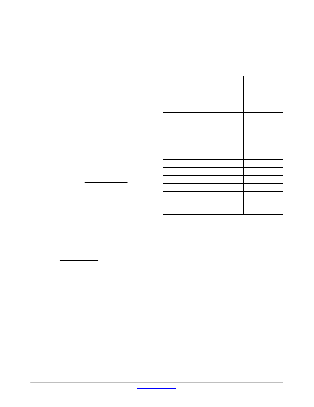
Table 9. PER PHASE OCP SETTINGS
Resistance
(kW)
10 65 4
14.7 75 4
20 100 4
26.1 134 4
33.2 65 6
41.2 75 6
49.9 100 6
60.4 134 6
71.5 65 8
84.5 75 8
100 100 8
118.3 134 8
136.6 65 10
157.7 75 10
182.1 100 10
249 134 10
NOTE: 1% tolerance.
Per Phase Voltage
(mV)
Latch Off Delay
(ms)
Under Voltage Lock-Out (VCC UVLO)
VCC is constantly monitored for the under voltage
lockout (UVLO) During power up both the VRMP and the
VCC pin are monitored Only after both pins exceed their
individual UVLO threshold will the full circuit be activated
and ready for the soft start ramp.
Over Voltage Protection
An output voltage monitor is incorporated into the
controller. During normal operation, if the output voltage is
400 mV over the REFIN value, the PGOOD pin will go low,
the DRON will assert low and the PWM outputs are set low.
The limit will be clamped at 2 V if REFIN is driven above
2 V. The outputs will remain disabled until the power is
cycled or the EN pin is toggled.
I2C Interface
The controller is connected to this bus as a slave device,
under the control of a master controller.
Data is sent over the serial bus in sequences of nine clock
pulses: eight bits of data followed by an acknowledge bit
from the slave device. Transitions on the data line must
occur during the low period of the clock signal and remain
stable during the high period, because a low-to-high
transition when the clock is high might be interpreted as
C
www.onsemi.com
16
Page 17

NCP81276
a stop signal. The number of data bytes that can be
transmitted over the serial bus in a single read or write
operation is limited only by what the master and slave
devices can handle.
The serial bus protocol operates as follows:
1. The master initiates data transfer by establishing
a START condition, defined as a high-to-low
transition on the serial data line SDA while the serial
clock line, SCL, remains high. This indicates that an
address/data stream will follow. All slave
peripherals connected to the serial bus respond to the
START condition, and shift in the next eight bits,
consisting of a 7-bit address (MSB first) plus an R/W
bit, which determines the direction of the data
transfer, i.e., whether data will be written to or read
from the slave device. The peripheral whose address
corresponds to the transmitted address responds by
pulling the data line low during the low period before
the ninth clock pulse, known as the Acknowledge
Bit. All other devices on the bus now remain idle
while the selected device waits for data to be read
from or written to it. If the R/W bit is a 0, the master
will write to the slave device. If the R/W bit is a 1, the
master will read from the slave device.
2. Data is sent over the serial bus in sequences of nine
clock pulses, eight bits of data followed by an
Acknowledge Bit from the slave device. Transitions
on the data line must occur during the low period of
the clock signal and remain stable during the high
period, as a low-to-high transition when the clock is
high may be interpreted as a STOP signal. The
number of data bytes that can be transmitted over the
serial bus in a single READ or WRITE operation is
limited only by what the master and slave devices
can handle.
3. When all data bytes have been read or written, stop
conditions are established. In WRITE mode, the
master will pull the data line high during the 10
clock pulse to assert a STOP condition. In READ
mode, the master device will override the
acknowledge bit by pulling the data line high during
the low period before the ninth clock pulse. This is
known as No Acknowledge. The master will then
take the data line low during the low period before
the tenth clock pulse, then high during the tenth
clock pulse to assert a STOP condition.
4. Any number of bytes of data may be transferred over
the serial bus in one operation, but it is not possible
to mix read and write in one operation because the
type of operation is determined at the beginning and
cannot subsequently be changed without starting
a new operation. To write data to one of the device
data registers or read data from it, the Address
Pointer Register must be set so that the correct data
register is addressed, and then data can be written
into that register or read from it. The first byte of
a write operation always contains an address that is
stored in the Address Pointer Register. If d at a i s t o b e
written to the device, the write operation contains
a second data byte that is written to the register
selected by the address pointer register. The device
address is sent over the bus followed by R/W set to
0. This is followed by two data bytes. The first data
byte is the address of the internal data register to be
written to, which is stored in the Address Pointer
Register. The second data byte is the data to be
written to the internal data register.
READ A SINGLE WORD
The master device asserts the start condition. The master
then sends the 7-bit slave address. It is followed by a R/W
bit that indicates the direction of operation, which will be
a write operation in this case. The slave whose address is on
the bus acknowledges it by an ACK signal on the bus (by
holding SDA line low). The master then sends register
address on the bus. The slave device accepts it by an ACK.
The master then asserts a repeated start condition followed
by a 7-bit slave address. The master then sends a direction
bit R/W which is Read for this case. Controller
acknowledges it b y an ACK signal on the bus. This will start
the read operation and controller sends the high byte of the
register on the bus. Master reads the high byte and asserts an
th
ACK on the SDA line. Controller now sends the low byte of
the register on the SDA line. The master acknowledges it by
a no acknowledge NACK on the SDA line. The master then
asserts the stop condition to end the transaction.
S 0 ACKSr 1 PNACKACK ACKSlave Address Register Address Slave Address Register Data
= Generated by the Master
= Generated by the Slave
S = Start Condition
P = Stop Condition
Figure 9. Single Register Read Operation
www.onsemi.com
Sr = Repeated Start Condition
ACK/NACK = Acknowledge/No Acknowledge
17
Page 18
NCP81276
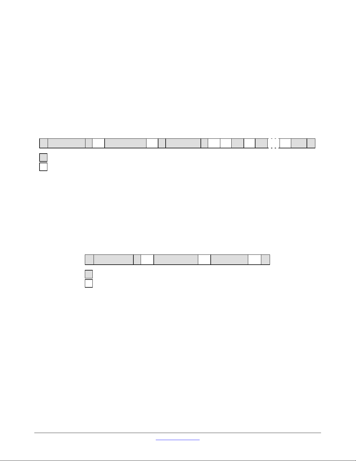
READING THE SAME REGISTERS
MULTIPLE TIMES
The master device asserts the start condition. The master
then sends the 7-bit slave address. It is followed by a R/W
bit that indicates the direction of operation, which will be
a write operation in this case. The slave whose address is on
the bus acknowledges it by an ACK signal on the bus
(holding SDA line low). The master then sends register
address on the bus. The slave device accepts it by an ACK.
The master then asserts a repeated start condition followed
by a 7-bit slave address. The master then sends a direction
bit R/W which is Read for this case. Slave device
acknowledges it b y an ACK signal on the bus. This will start
the read operation:
S Slave Address 0 ACK Register Address Sr Slave AddressACK 1 ACK RD1 NACK PACK RD2 ACK RDN
= Generated by the Master
= Generated by the Slave
S = Start Condition
P = Stop Condition
Figure 10. Multiple Register Read Operation
Sr = Repeated Start Condition
ACK/NACK = Acknowledge/No Acknowledge
1. The slave device sends the high byte of the register
on the bus.
2. The master reads the high byte and asserts an ACK
on the SDA line.
3. The slave device now sends the low byte of the
register on the SDA line.
4. The master acknowledges it by an ACK signal on the
SDA line.
5. The master and slave device keeps on repeating steps
1−4 until the low byte of the last reading is
transferred. After receiving the low byte of the last
register, the master asserts a not acknowledge
NACK on the SDA. The master then asserts a stop
condition to end the transaction.
RD1…N = Register Data 1…N
WRITING A SINGLE WORD
The master device asserts the start condition. The master
then sends the 7-bit to the slave address. It is followed by a
R/W bit that indicates the direction of operation, which will
be a write operation in this case. The slave whose address is
on the bus acknowledges it by an ACK signal on the bus (by
holding SDA line low). The master then sends register
The master then sends a data byte of the high byte of the
register. The slave device asserts an acknowledge ACK on
the SDA line. The master then sends a data byte of the low
byte of the register. The slave device asserts an acknowledge
ACK on the SDA line. The master asserts a stop condition
to end the transaction.
address on the bus. The slave device accepts it by an ACK.
S Slave Address 0 ACK Register Address Register DataACK PACK
= Generated by the Master
= Generated by the Slave
Figure 11. Single Register Write Operation
S = Start Condition
P = Stop Condition
WRITING MULTIPLE WORDS TO
DIFFERENT REGISTERS
The master device asserts the start condition. The master
then sends the 7-bit slave address. It is followed by a bit
(R/W) that indicates the direction of operation, which will
be a write operation in this case. The slave whose address is
on the bus acknowledges it by an ACK signal on the bus (by
holding SDA line low).
The master then sends first register address on the bus.
The slave device accepts it by an ACK. The master then
sends a data byte of the high byte of the first register. The
slave device asserts an acknowledge ACK on the SDA line.
The master then sends a data byte of the low byte of the first
register. The slave device asserts an acknowledge ACK on
the SDA line.
ACK = Acknowledge
The master then sends the second register address on the
bus. The slave device accepts it by an ACK. The master then
sends a data byte of the high byte of the second register. The
slave device asserts an acknowledge ACK on the SDA line.
The master then sends a data byte of the low byte of the
second register. The slave device asserts an acknowledge
ACK on the SDA line.
A complete word must be written to a register for proper
operation. It means that both high and low bytes must be
written.
www.onsemi.com
18
Page 19
NCP81276
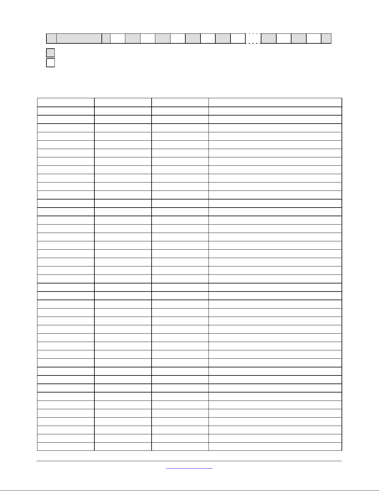
S Slave Address 0 ACK RA1 ACK PRD1 ACK RA2 ACK RD2 ACK RAN ACK RDN ACK
= Generated by the Master
= Generated by the Slave
Table 10. REGISTER MAP
Address
0x20 R/W 0xFF IOUT_OC_WARN_LIMIT
0x21 R 0x00 STATUS BYTE
0x22 R/W 0x00 Fault Mask
0x23 R 0x00 STATUS Fault
0x24 R 0x00 STATUS Warning
0x26 R 0x00 READ_IOUT
0x27 R 0x1A MFR_ID
0x28 R 0x76 MFR_MODEL
0x29 R 0x04 MFR_REVISION
0x2A R/W 0x00 Lock/Reset
0x2B R 0x00 Soft Start Status
0x2C N/A 0x00 Reserved
0x2D R OCP Status
0x2E R/W 0x00 OCP Configuration
0x2F R Switching Frequency Status
0x30 R/W 0x00 Switching Frequency Configuration
0x31 N/A 0x00 Reserved
0x32 R PSI Status
0x33 R Phase Status
0x34 R/W 0x1F LPC_Zone_enable
0x35 R LPC Status
0x36 R/W 0x00 LPC Configuration
0x38 R LL Status
0x39 R/W 0x03 LL Configuration
0x3A RW 0x00 PHTH1 Configuration
0x3B R PHTH1 Status
0x3C R/W 0x00 PHTH2 Configuration
0x3D R PHTH2 Status
0x3E R/W 0x00 PHTH3 Configuration
0x3F R PHTH3 Status
0x40 R/W 0x00 PHTH4 Configuration
0x41 R PHTH4 Status
0x44 R/W 0x08 Phase Shedding Hysteresis
0x45 R/W 0x14 Phase Shedding Delay
0x46 R/W 0x00 Second Function Configuration Register Latch A
0x47 R/W 0x00 Second Function Configuration Register Latch B
0x48 N/A N/A Reserved
0x49 N/A N/A Reserved
0x4A N/A N/A Reserved
0x4B N/A N/A Reserved
0x4C N/A N/A Reserved
S = Start Condition
P = Stop Condition
RD1…N = Register Data 1…N
ACK = AcknowledgeRA1…N = Register Address 1…N
Figure 12. Multiple Register Write Operation
R/W Default Value Description
www.onsemi.com
19
Page 20

NCP81276
IOUT_OC_WARN_LIMIT Register (0x20)
This sets the high current limit. Once the READ_IOUT
register value exceeds this limit IOUT_OC_WARN_LIMIT
bit is set in the Status Warning register and an ALERT is
generated.
STATUS BYTE Register (0x21)
Table 11. STATUS BYTE REGISTER SETTINGS
Bits Name Description
7:6 Reserved N/A
5 VOUT_OV This bit gets set whenever the
NCP81276 goes into OVP mode.
4 IOUT_OC This bit gets set whenever the
NCP81276 latches off due to an over
current event.
0:3 Reserved N/A
Fault Mask Register (0x22)
Table 12. FAULT MASK REGISTER SETTINGS
Bits Name Description
7:5 Reserved
4 Clim1 When this bit is set, the Clim1 bit from
the STATUS FAULT register is
cleared.
3 Clim2 When this bit is set, the Clim2 bit from
the STATUS FAULT register is
cleared.
2 Clim_phase When this bit is set, the Clim_phase
bit from the STATUS FAULT register
is cleared.
1 OVP When this bit is set, the OVP bit from
the STATUS FAULT register is
cleared.
0 UVP When this bit is set, the UVP bit from
the STATUS FAULT register is
cleared.
STATUS Fault Register (0x23)
Table 13. STATUS FAULT REGISTER SETTINGS
Bits Name Description
7:5 Reserved N/A
4 Clim1 This bit gets set when IOUT exceeds
3 Clim2 This bit gets set when IOUT exceeds
2 Clim_phase This bit gets set when the phase
1 OVP This bit is set when an OVP event is
0 UVP his bit is set when an UVP event is
the ILIM value and its corresponding
bit from the fault mask register is set.
the ILIM value and its corresponding
bit from the fault mask register is set.
Current (V
OCP configuration value and its
corresponding bit from the fault mask
register is set.
detected and its corresponding bit
from the fault mask register is set.
detected and its corresponding bit
from the fault mask register is set.
CSN−VCSREF
) exceeds the
STATUS Warning Register (0x24)
Table 14. STATUS WARNING REGISTER SETTINGS
Bits Name Description
7:1 Reserved N/A
0 IOUT Overcurrent
Warning Reserved
This bit gets set if IOUT
exceeds its programmed high
warning limit(register 0x20).
This bit is only cleared when
EN is toggled.
READ_IOUT Register (0x26)
Read back output current. ADC conversion 0xFF = 2 V
on IOUT pin which should equate to max current.
Lock/Reset Register (0x2A)
Table 15. LOCK/RESET REGISTER SETTINGS
Bits Name Description
7:1 Reserved N/A
0 Lock Logic 1 locks all limit values to their
current settings. Once this bit is set,
all lockable registers become
read-only and cannot be modified
until the NCP81276 is powered down
and powered up again. This prevents
rogue programs such as viruses from
modifying critical system limit settings
(Lockable).
www.onsemi.com
20
Page 21
NCP81276
Soft Start Status Register (0x2B)
This register contains the value that sets the slew rate of
the output voltage during power-up. When EN is set high,
the controller reads the value of the resistor connected to the
SS pin and sets the slew rate. The codes corresponding to
each resistor setting are shown in Table 16. The resistor
settings are updated on every rising edge of the EN signal.
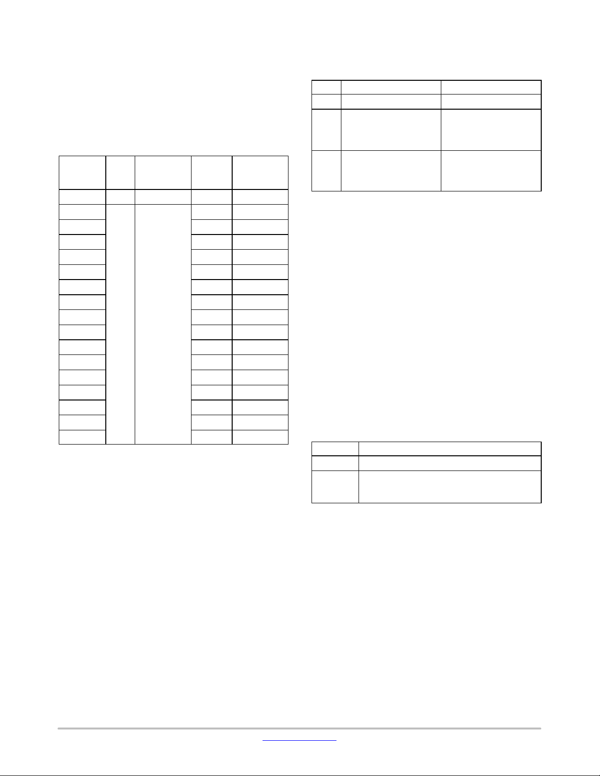
Table 16. SOFT START STATUS REGISTER SETTINGS
T
RAMP
Resistor
(kW)
− 7:4 Reserved N/A N/A
10
14.7 0001 0.3
20 0010 0.45
26.1 0011 0.6
33.2 0100 0.75
41.2 0101 0.9
49.9 0110 1
60.4 0111 2
71.5 1000 3
84.5 1001 4
100 1010 5
118.3 1011 6
136.6 1100 7
157.7 1101 8
182.1 1110 9
249 1111 10
NOTE: 1% tolerance.
Bits Name Value
3:0 T_Ramp
0000 0.15
T_ramp
(ms)
OCP Status Register and Configuration Register
(0x2D, 0x2E)
These registers contain the values that set the OCP current
levels for each phase individually as well as the latch off
delay time for the OCP event. When EN is set high, the
controller reads the value of the resistor connected to the
OCP pin and sets the OCP threshold and latch off delay time
according to Table 9. The codes corresponding to each
setting are shown in Table 17. The resistor settings are
updated on every rising edge of the EN signal.
The OCP configuration register allows the user to
dynamically change the OCP threshold and latch off delay
through the I
2
C interface provided that the OCP bits from
the second function configuration registers A and B (0x46,
0x47) are set. In addition, the OCP levels and latch off delay
times can be adjusted independently when the OCP
configuration register is used. The achievable switching
frequency settings are listed in Table 17.
Table 17. OCP STATUS AND CONFIGURATION
REGISTER SETTINGS
Bits Name Description
7:4 Reserved N/A
3:2 Per Phase OCP Limit 00 = 65 mV
1:0 OCP_latch Off Delay 00 = 4 ms
01 = 75 mV
10 = 100 mV
11 = 134mV
01 = 6 ms
10 = 8 ms
11 = 10ms
Switching Frequency Status and Configuration
Registers (0x2F, 0x30)
These registers contain the values that set the switching
frequency of the controller. When EN is set high, the
controller reads the value of the resistor connected to the
FSW pin and sets the switching frequency according to
Table19. The codes corresponding to each setting are also
shown in Table 19. The resistor settings are updated on
every rising edge of the EN signal.
The switching frequency configuration register allows the
user to dynamically change the switching frequency through
2
the I
C interface provided that the FSW bits from the second
function configuration registers A and B (0x46, 0x47) are
set.
PSI Status Register (0x32)
The PSI status register provides the information regarding
the current status of the PSI pin though the I
2
C interface as
shown in Table 18.
Table 18. PSI STATUS REGISTER SETTINGS
Bits Description
7:2 Reserved
1:0 00 = PSI MID
01 = PSI LOW
10 = PSI HIGH
www.onsemi.com
21
Page 22
NCP81276
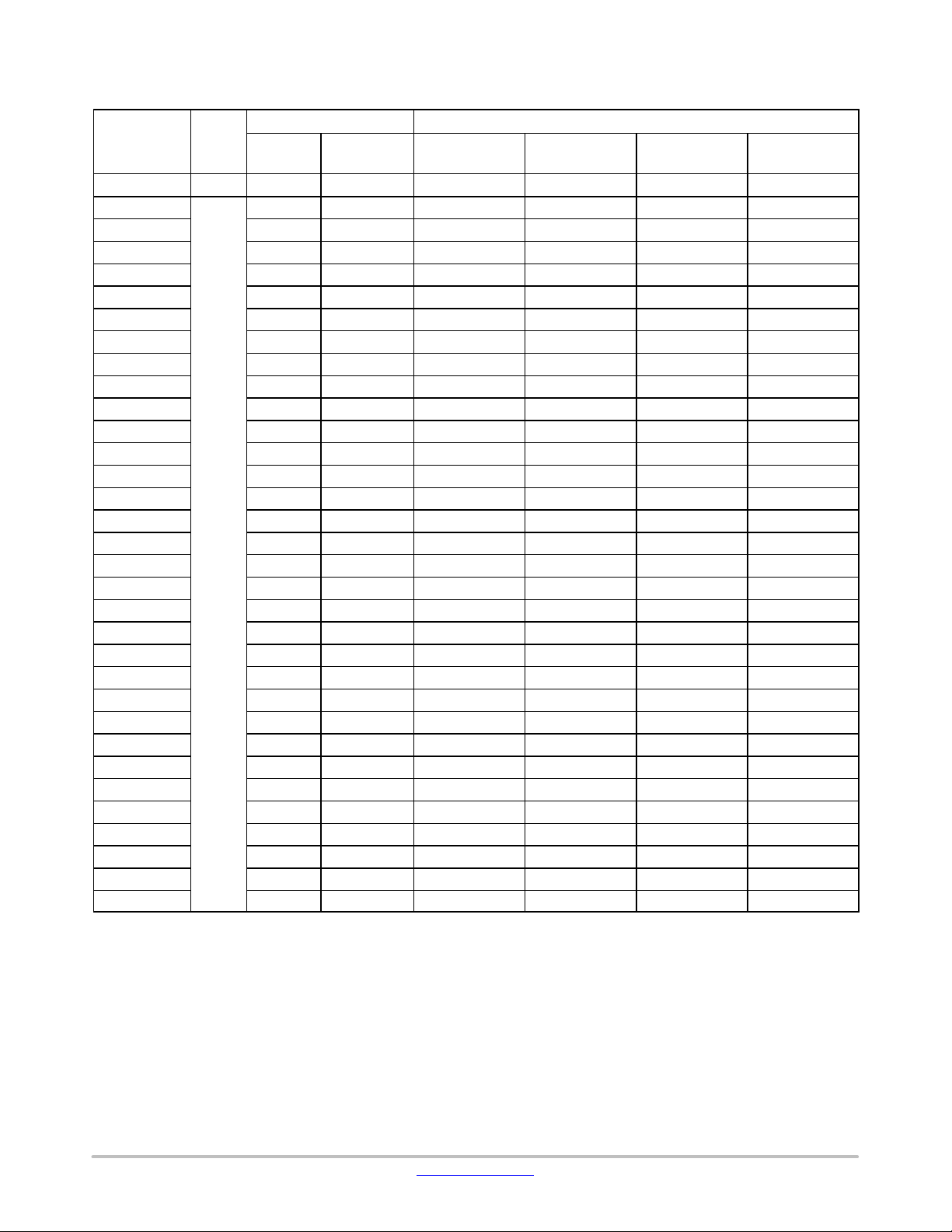
Table 19. SWITCHING FREQUENCY STATUS AND CONFIGURATION REGISTER SETTINGS
FSW Pin
Resistor
Value (kW)
10
14.7
20
26.1
33.2
41.2
49.9
60.4 01110 01110 518 688 526 518
71.5 10000 10000 581 789 583 578
84.5 10010 10010 708 930 698 698
100 10100 10100 799 1095 807 818
118.3 10110 10110 919 1233 899 938
136.6 11000 11000 993 1341 1003 1014
157.7 11010 11010 1098 1450 1096 1106
182.1 11100 11100 1200 1619 1205 1201
249 11110 11110 1291 1674 1274 1280
NOTE: 1% tolerance.
Bits
7:5 Reserved Reserved N/A N/A N/A N/A
4:0
Status
Register
00000 00000 221 293 223 232
00010 00010 266 358 264 272
00100 00100 307 407 317 322
00110 00110 351 480 352 361
01000 01000 394 530 399 413
01010 01010 449 600 436 456
01100 01100 479 631 483 500
Value Switching Frequency (kHz)
Configuration
Register
− 00001 244 329 243 252
− 00011 293 381 294 297
− 00101 333 450 335 340
− 00111 373 510 380 385
− 01001 421 562 420 435
− 01011 469 614 454 478
− 01101 509 663 508 509
− 01111 543 722 543 540
− 10001 649 859 656 638
− 10011 751 1010 771 758
− 10101 866 1147 860 878
− 10111 964 1260 950 972
− 11001 1059 1372 1052 1067
− 11011 1141 1539 1154 1155
− 11101 1236 1618 1227 1245
− 11111 1312 1724 1316 1330
4
Phase
3
Phase
2
Phase
1
Phase
www.onsemi.com
22
Page 23
NCP81276
Phase Status Register (0x33)
The Phase Status register provides the information about
the status of each of the four available phases as shown in
Table20.
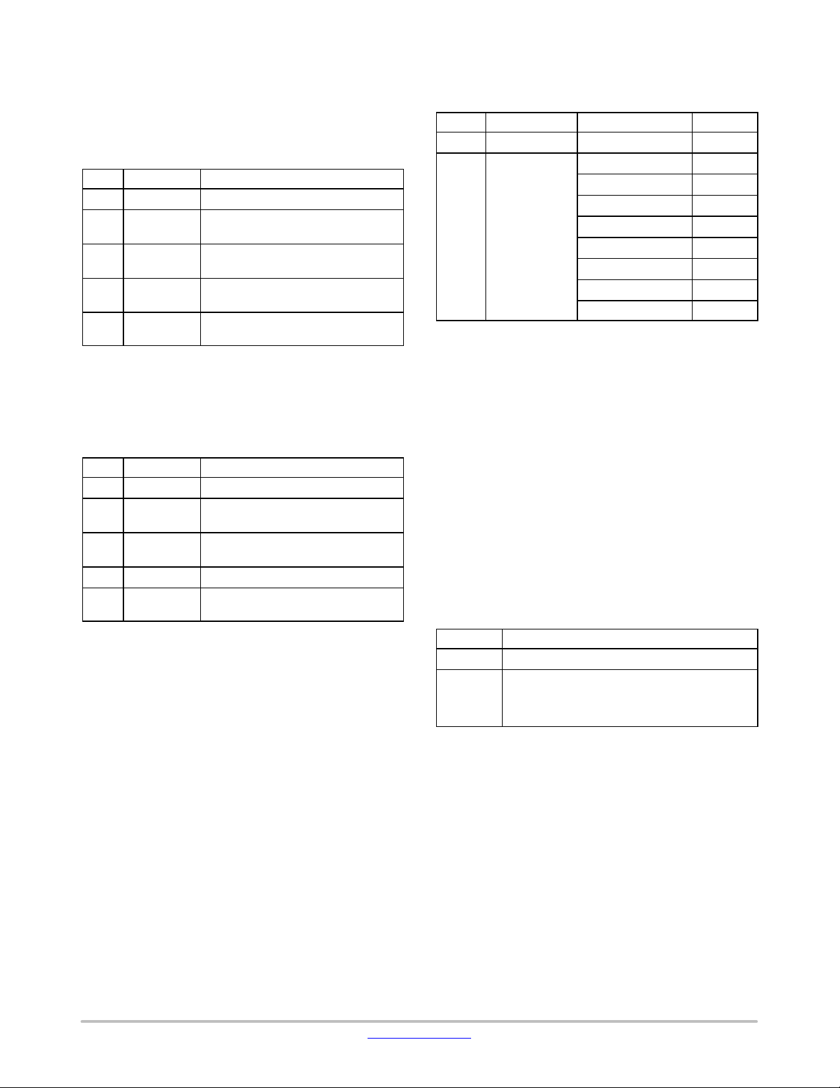
Table 20. PHASE STATUS REGISTER SETTINGS
Bits Name Description
7:4 Reserved N/A
3 Phase 4 0 = Disabled
2 Phase 3 0 = Disabled
1 Phase 2 0 = Disabled
0 Phase 1 0 = Disabled
LPC_Zone_enable Register (0x34)
1 = Enabled
1 = Enabled
1 = Enabled
1 = Enabled
The LPC_Zone_enable register allows the user to enable
or disable power zones while the controller has the PSI set
low using the I
Table 21. LPC_ZONE_ENABLE REGISTER SETTINGS
Bits Name Description
7:4 Reserved N/A
3 Zone 4 0 = Disabled
2 Zone 3 0 = Disabled
1 Reserved N/A
0 Zone 1 0 = Disabled
LPC Status and Configuration Registers (0x35, 0x36)
2
C interface as shown in Table 21.
1 = Enabled
1 = Enabled
1 = Enabled
These registers contain the values that set the operating
power zone when the PSI pin is set low . When EN is set high,
the controller reads the value of the resistor connected to the
LPC1 and LPC2 pins and sets the power zone according to
Table7. The codes corresponding to each setting are shown
in Table 22. The LPC
resistor settings are updated on every
X
rising edge of the EN signal.
The LPC configuration register allows the user to
dynamically change the power zone (PSI = Low) through
2
the I
C interface provided that the LPC bits from the second
function configuration registers A and B (0x46, 0x47) are
set. The achievable power zone settings are listed in
Table22.
Table 22. LPC STATUS AND CONFIGURATION
REGISTER SETTINGS
Bits Name Value Level
7:3 Reserved N/A N/A
2:0 LPC1
Configuration
LL Status and Configuration Registers (0x38, 0x39)
000 0
001 1
010 = Reserved N/A
011 3
100 4
101 = Reserved N/A
110 = Reserved N/A
111 = Reserved N/A
These registers contain the values that set the fraction of
the externally configured load line (see Total Current Sense
Amplifier section) to be used during the normal operation of
the device. When EN is set high, the controller reads the
value of the resistor connected to the LL/I2C_ADD pin and
sets the load line according to Table 5. The codes
corresponding to each setting are shown in Table 23. The
load line resistor setting is updated on every rising edge of
the EN signal.
The LL configuration register allows the user to
dynamically change the load line settings through the I
2
interface provided that the LL bits from the second function
configuration registers A and B (0x46, 0x47) are set. The
achievable load line settings are listed in Table 23.
Table 23. LL STATUS AND CONFIGURATION
REGISTER SETTINGS
Bits Description
7:2 Reserved
1:0 00 = 100% of externally set load line (default)
PHTH1 to PHTH4 Configuration Registers
(0x3A, 0x3C, 0x3E, 0x40)
01 = 50% of externally set load line
10 = 25 of externally set load line
11 = 0% of externally set load line
These registers contain the values that control the phase
shedding thresholds and are active when the PHTH
X
bits
from the second function configuration registers A and B
(0x46 and 0x47) are set be set. These thresholds allow the
user to dynamically change the thresholds through the I
2
interface. The values written to these registers should match
the value of the READ_IOUT register (0x26) at the desired
load current. If 0xFF is written to a register, the phase
shedding threshold corresponding to that register is
disabled.
C
C
www.onsemi.com
23
Page 24

NCP81276
PHTH1 to PHTH4 Status Registers
(0x3B, 0x3D, 0x3F 0x41)
These registers contain the phase shedding threshold
values set by the resistors connected to the PHTH
pins. The
X
values of the thresholds are updated on every rising edge of
the EN signal. The resistor values should be chosen to ensure
that the voltage drop across them developed by the 10 mA
current sourced by the NCP81276 during power-up (EN set
high) matches the value of the READ_IOUT register (0x26)
at the desired load current. Setting the resistors to generate
a voltage above 2 V will disable the PHTH
threshold for
X
that pin.
Phase Shedding Hysteresis Register (0x44)
This register sets the hysteresis during a transition from
a high count phase to a low count phase configuration. The
hysteresis is expressed in codes (LSBs) of the PHTH
threshold values.
Phase Shedding Delay Register (0x45)
This register sets the delay during a transition from a high
count phase to a low count phase configuration. The
power-up default value is 200 ms and it can be dynamically
2
changed in steps of 10 ms (1 LSB) through the I
C interface.
Second Function Configuration Register
Latch A and B Registers (0x46, 0x47)
These registers allow the user to select whether the second
functions settings (LL, Soft Start, OCP, LPC and PHTH
X
are controlled by the external resistors or the configuration
registers (see Table 24). When/EN is toggled the default
control mode for the second functions is the external resistor .
Switching between the two modes can be done by simply
writing the appropriate byte (the same byte) to both registers
(the order doesn’t matter).
Table 24. SECOND CONFIGURATION LATCH
REGISTER A AND B
Second Function
Configuration
Bits
7:6 Reserved N/A
5 FSW 0 = set by external resistor
4 LL 0 = set by external resistor
3 Reserved N/A
2 OCP 0 = set by external resistor
X
1 Reserved N/A
0 PHTH
Register
Description
(see Table 19)
1 = set by register 0x30
(see Table 19)
(see Table 5)
1 = set by register 0x39
(see Table 9)
1= set by register 0x2E
X
0 = set by external resistors
connected between PHTH
and GND
1 = set by registers 0x3A, 0x3C,
0x3E and 0x40
X
pins
)
NVIDIA is a registered trademark of of NVIDIA Corporation in the U.S. and/or other countries. All other brand names and product names appearing in this document
are registered trademarks or trademarks of their respective holders.
www.onsemi.com
24
Page 25
ÉÉ
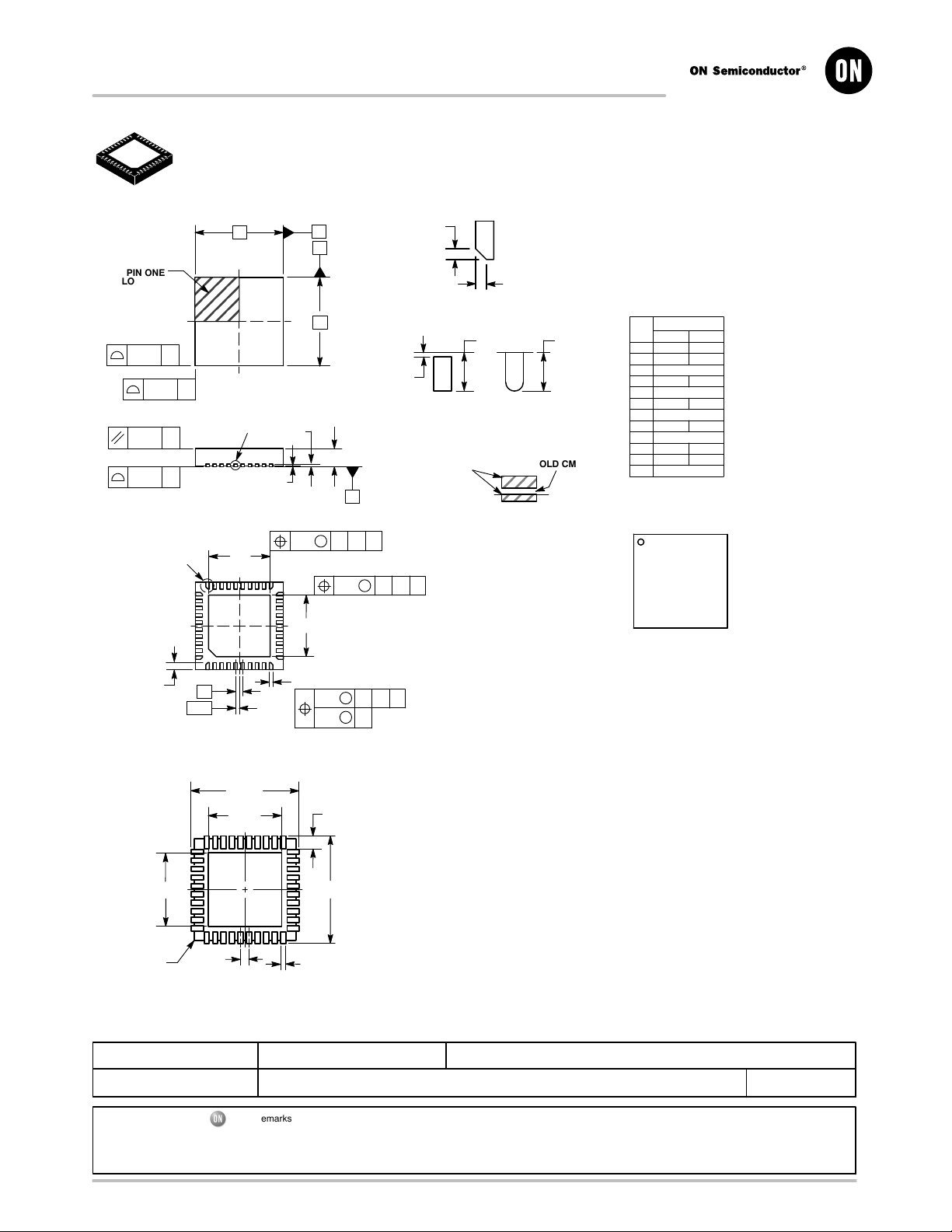
MECHANICAL CASE OUTLINE
PACKAGE DIMENSIONS
401
SCALE 2:1
A1
(A3)
21
40X
E2
A
B
E
M
b
0.05
A
40X
0.63
C
M
M
SEATING
PLANE
A0.10 BC
M
C
A0.10 BC
NOTE 3
PIN ONE
LOCATION
NOTE 4
D
0.15 C
0.15
C
TOP VIEW
0.10 C
DETAIL B
0.08 C
SIDE VIEW
D2
11
1
40
e
40X
DETAIL A
L
e/2
BOTTOM VIEW
RECOMMENDED
SOLDERING FOOTPRINT
5.30
3.64
QFN40 5x5, 0.4P
CASE 485CR
ISSUE C
L2
DETAIL A
L1
DETAIL A
ALTERNATE TERMINAL
CONSTRUCTIONS
A0.10 BC
L2
L
MOLD CMPDEXPOSED Cu
DETAIL B
ALTERNATE
CONSTRUCTION
DATE 27 AUG 2013
NOTES:
1. DIMENSIONING AND TOLERANCING PER
ASME Y14.5M, 1994.
2. CONTROLLING DIMENSIONS: MILLIMETERS.
3. DIMENSION b APPLIES TO PLATED
TERMINAL AND IS MEASURED BETWEEN
0.15 AND 0.30mm FROM THE TERMINAL TIP.
4. COPLANARITY APPLIES TO THE EXPOSED
PAD AS WELL AS THE TERMINALS.
MILLIMETERS
L
DIM MIN MAX
A 0.80 1.00
A1 −−− 0.05
A3 0.20 REF
b 0.15 0.25
D 5.00 BSC
D2 3.40 3.60
E 5.00 BSC
e 0.40 BSC
L 0.30 0.50
L1 −−− 0.15
L2 0.12 REF
3.60E2 3.40
GENERIC
MARKING DIAGRAM*
1
XXXXXXXX
XXXXXXXX
AWLYYWWG
G
XXXXX = Specific Device Code
A = Assembly Location
WL = Wafer Lot
YY = Year
WW = Work Week
G = Pb−Free Package
(Note: Microdot may be in either location)
*This information is generic. Please refer
to device data sheet for actual part
marking.
Pb−Free indicator, “G” or microdot “ G”,
may or may not be present.
1
40X
0.25
5.30
Electronic versions are uncontrolled except when accessed directly from the Document Repository.
Printed versions are uncontrolled except when stamped “CONTROLLED COPY” in red.
PAGE 1 OF 1
www.onsemi.com
3.64
PKG
OUTLINE
DOCUMENT NUMBER:
ON Semiconductor and are trademarks of Semiconductor Components Industries, LLC dba ON Semiconductor or its subsidiaries in the United States and/or other countries.
ON Semiconductor reserves the right to make changes without further notice to any products herein. ON Semiconductor makes no warranty, representation or guarantee regarding
the suitability of its products for any particular purpose, nor does ON Semiconductor assume any liability arising out of the application or use of any product or circuit, and specifically
disclaims any and all liability, including without limitation special, consequential or incidental damages. ON Semiconductor does not convey any license under its patent rights nor the
rights of others.
© Semiconductor Components Industries, LLC, 2019
0.40
PITCH
DIMENSIONS: MILLIMETERS
DESCRIPTION:
98AON83971E
QFN40, 5x5, 0.4P
Page 26

onsemi, , and other names, marks, and brands are registered and/or common law trademarks of Semiconductor Components Industries, LLC dba “onsemi” or its affiliates
and/or subsidiaries in the United States and/or other countries. onsemi owns the rights to a number of patents, trademarks, copyrights, trade secrets, and other intellectual property.
A listing of onsemi’s product/patent coverage may be accessed at www.onsemi.com/site/pdf/Patent−Marking.pdf. onsemi reserves the right to make changes at any time to any
products or information herein, without notice. The information herein is provided “as−is” and onsemi makes no warranty, representation or guarantee regarding the accuracy of the
information, product features, availability, functionality, or suitability of its products for any particular purpose, nor does onsemi assume any liability arising out of the application or use
of any product or circuit, and specifically disclaims any and all liability, including without limitation special, consequential or incidental damages. Buyer is responsible for its products
and applications using onsemi products, including compliance with all laws, regulations and safety requirements or standards, regardless of any support or applications information
provided by onsemi. “Typical” parameters which may be provided in onsemi data sheets and/or specifications can and do vary in different applications and actual performance may
vary over time. All operating parameters, including “Typicals” must be validated for each customer application by customer’s technical experts. onsemi does not convey any license
under any of its intellectual property rights nor the rights of others. onsemi products are not designed, intended, or authorized for use as a critical component in life support systems
or any FDA Class 3 medical devices or medical devices with a same or similar classification in a foreign jurisdiction or any devices intended for implantation in the human body. Should
Buyer purchase or use onsemi products for any such unintended or unauthorized application, Buyer shall indemnify and hold onsemi and its officers, employees, subsidiaries, affiliates,
and distributors harmless against all claims, costs, damages, and expenses, and reasonable attorney fees arising out of, directly or indirectly, any claim of personal injury or death
associated with such unintended or unauthorized use, even if such claim alleges that onsemi was negligent regarding the design or manufacture of the part. onsemi is an Equal
Opportunity/Affirmative Action Employer. This literature is subject to all applicable copyright laws and is not for resale in any manner.
PUBLICATION ORDERING INFORMATION
LITERATURE FULFILLMENT:
Email Requests to: [email protected]
onsemi Website: www.onsemi.com
TECHNICAL SUPPORT
North American Technical Support:
Voice Mail: 1 800−282−9855 Toll Free USA/Canada
Phone: 011 421 33 790 2910
Europe, Middle East and Africa Technical Support:
Phone: 00421 33 790 2910
For additional information, please contact your local Sales Representative
◊
 Loading...