

Page 1
ADT7473
dBCOOLR Remote Thermal
Monitor and Fan Control
The ADT7473/ADT7473−1 dBCOOL controller is a thermal
monitor and multiple PWM fan controller for noise sensitive or power
sensitive applications requiring active system cooling. The
ADT7473/ADT7473−1 can drive a fan using either a low or high
frequency drive signal, monitor the temperature of up to two remote
sensor diodes plus its own internal temperature, and measure and
control the speed of up to four fans so they operate at the lowest
possible speed for minimum acoustic noise.
The automatic fan speed control loop optimizes fan speed for a
given temperature. A unique dynamic T
system thermals/acoustics to be intelligently managed. The
effectiveness of the system’s thermal solution can be monitored using
the THERM
input. The ADT7473/ADT7473−1 also provide critical
thermal protection to the system using the bidirectional THERM
as an output to prevent system or component overheating.
FEATURES
• Controls and Monitors Up to 4 Fans
• High and Low Frequency Fan Drive Signal
• 1 On−Chip and 2 Remote Temperature Sensors
• Series Resistance Cancellation on the Remote Channel
• Extended Temperature Measurement Range, Up to 191°C
• Dynamic T
Acoustics
Control Mode Intelligently Optimizes System
MIN
• Automatic Fan Speed Control Mode Controls System Cooling Based
on Measured Temperature
• Enhanced Acoustic Mode Dramatically Reduces User Perception of
Changing Fan Speeds
• Thermal Protection Feature via THERM Output
• Monitors Performance Impact of Intel Pentium
• Thermal Control Circuit via THERM Input
• 3−Wire and 4−Wire Fan Speed Measurement
• Limit Comparison of All Monitored Values
• Meets SMBus 2.0 Electrical Specifications
(Fully SMBus 1.1 Compliant)
• This is a Pb−Free Device
• Fully RoHS Compliant
control mode enables the
MIN
R
4 Processor
pin
http://onsemi.com
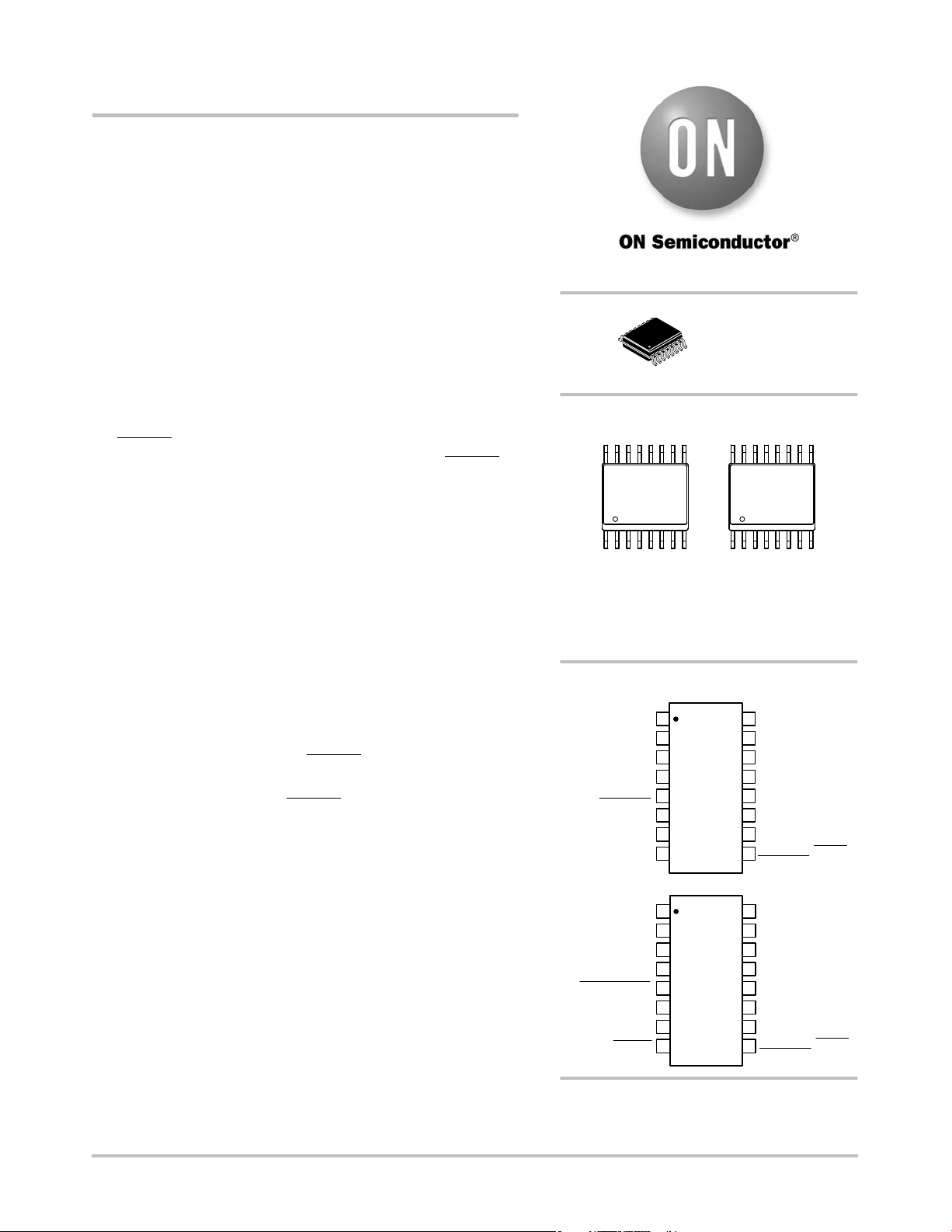
MARKING DIAGRAMS
ADT747
3ARQZ
#YYWW
xxxx
ADT7473 ADT7473−1
# = Pb−Free Package
YYWW = Date Code
xx = Assembly Lot
PIN ASSIGNMENTS
SCL
1
GND
2
V
3
CC
4
TACH3
PWM2/
SMBALERT
TACH1
TACH2
PWM3
GND
TACH3/
ADDR SELECT
THERM_LATCH/
PWM2
TACH1
TACH2
PWM3/ADDREN
SCL
V
CC
ADT7473
TOP VIEW
5
6
7
8
1
2
3
4
ADT7473−1
TOP VIEW
5
6
7
8
QSOP−16
CASE 492
ADT
7473−1
ARQZ
xxxx
SDA
16
PWM1/XTO
15
V
14
CCP
13
D1+
12
D1–
D2+
11
D2–
10
TACH4/GPIO/THERM
9
SMBALERT
16
SDA
PWM1/XTO
15
V
14
CCP
13
D1+
D1–
12
D2+
11
D2–
10
TACH4/GPIO/THERM
9
SMBALERT
© Semiconductor Components Industries, LLC, 2009
April, 2009 − Rev. 6
ORDERING INFORMATION
See detailed ordering and shipping information in the package
dimensions section on page 73 of this data sheet.
1 Publication Order Number:
ADT7473/D
Page 2
ADT7473
PWM1
PWM2
PWM3
TACH1
TACH2
TACH3
TACH4
*THERM_LATCH
V
D1+
D1–
D2+
D2–
V
CCP
ADT7473/ADT7473−1
PWM
REGISTERS
AND
CONTROLLERS
(HF AND LF)
VCC TO ADT7473/ADT7473−1
CC
SRC
BAND GAP
TEMP SENSOR
ADDRESS
SELECTION
ACOUSTIC
ENHANCEMENT
CONTROL
FAN
SPEED
COUNTER
PERFORMANCE
MONITORING
THERMAL
PROTECTION
INPUT
SIGNAL
CONDITIONING
AND
ANALOG
MULTIPLEXER
*ADDR SELECT*ADDREN
SMBus
AUTOMATIC
FAN SPEED
CONTROL
DYNAMIC
T
MIN
CONTROL
10−BIT
ADC
BAND GAP
REFERENCE
SCL
SDA SMBALERT
SERIAL BUS
INTERFACE
ADDRESS
POINTER
REGISTER
PWM
CONFIGURATION
REGISTERS
INTERRUPT
MASKING
INTERRUPT
STATUS
REGISTERS
LIMIT
COMPARATORS
VALUE AND
LIMIT
REGISTERS
GND
*PIN FUNCTION ONLY AVAILABLE ON THE ADT7473−1
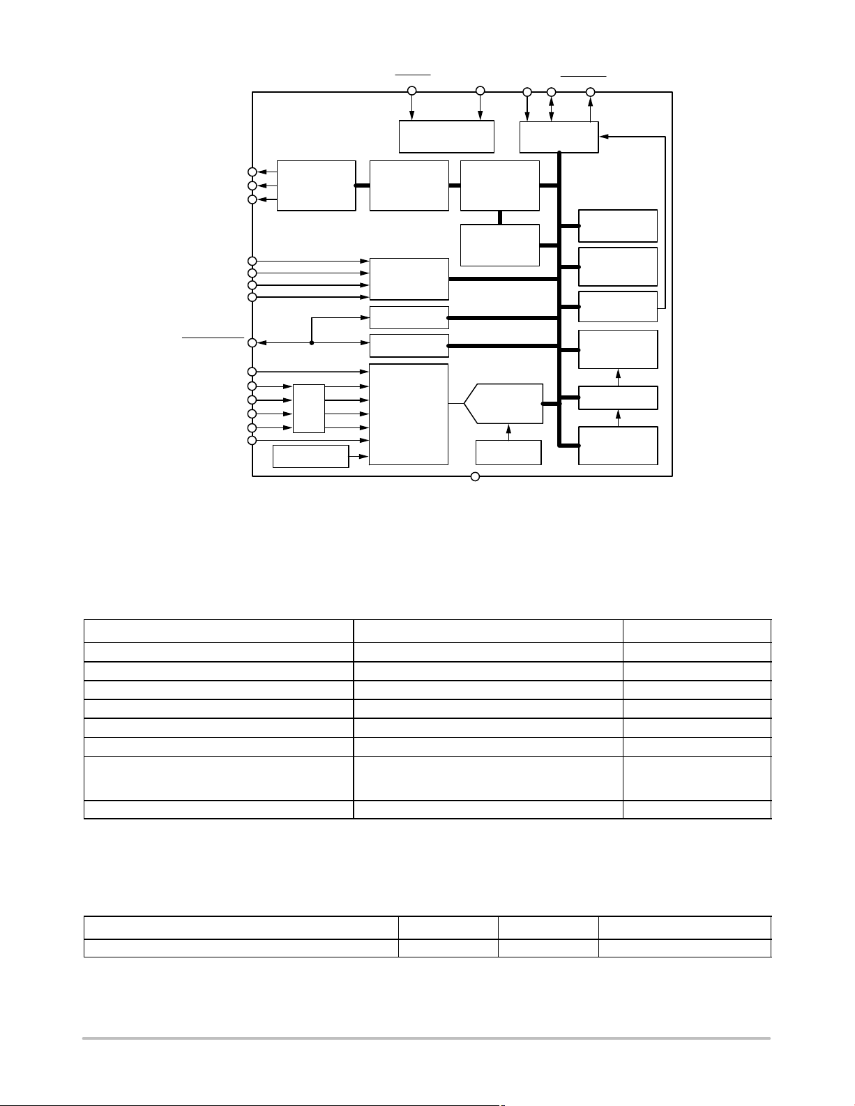
Figure 1. Functional Block Diagram
ABSOLUTE MAXIMUM RATINGS
Parameter Rating Unit
Positive Supply Voltage (VCC) 3.6 V
Voltage on any Input or Output Pin −0.3 to +3.6 V
Input Current at any Pin ±5.0 mA
Package Input Current ±20 mA
Maximum Junction Temperature (T
Storage Temperature Range −65 to +150 °C
Lead Temperature, Soldering
IR Reflow Peak Temperature
Lead Temperature (Soldering, 10 sec)
ESD Rating 1500 V
Stresses exceeding Maximum Ratings may damage the device. Maximum Ratings are stress ratings only. Functional operation above the
Recommended Operating Conditions is not implied. Extended exposure to stresses above the Recommended Operating Conditions may affect
device reliability.
NOTE: This device is ESD sensitive. Use standard ESD precautions when handling.
) 150 °C
J max
260
300
°C
THERMAL CHARACTERISTICS
Package Type
q
JA
q
JC
16−lead QSOP 150 39 °C/W
NOTE: qJA is specified for the worst−case conditions, that is, a device soldered in a circuit board for surface−mount packages.
Unit
http://onsemi.com
2
Page 3
ADT7473
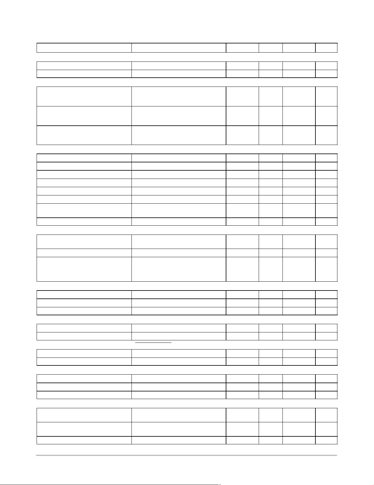
ELECTRICAL CHARACTERISTICS T
Parameter
A
= T
MIN
to T
MAX
, VCC = V
MIN
to V
, unless otherwise noted. (Note 1)
MAX
Conditions Min Typ Max Unit
Power Supply
Supply Voltage
Supply Current, I
CC
Interface inactive, ADC active 1.5 3.0 mA
3.0 3.3 3.6 V
Temperature−to−Digital Converter
Local Sensor Accuracy
0°C ≤ TA ≤ 85°C
−40°C ≤ TA ≤ +125°C
Resolution
Remote Diode Sensor Accuracy
Resolution
0°C ≤ TA ≤ 85°C
−40°C ≤ T
A
Remote Sensor Source Current First Current
Second Current
Third Current
≤ +125°C
±0.5
0.25
±0.5
0.25
6
36
96
±1.5
±2.5
±1.5
±2.5
Analog−to−Digital Converter (Including MUX and Attentuators)
Total Unadjusted Error (TUE)
±1.5 %
Differential Nonlinearity (DNL) 8 bits ±1.0 LSB
Power Supply Sensitivity ±0.1 %/V
Conversion Time (Voltage Input) Averaging enabled 11 ms
Conversion Time (Local Temperature) Averaging enabled 12 ms
Conversion Time (Remote Temperature) Averaging enabled 38 ms
Total Monitoring Cycle Time Averaging enabled
Averaging disabled
Input Resistance For V
channel 70 120
CCP
145
19
ms
kW
Fan RPM−to−Digital Converter
Accuracy
0°C ≤ TA ≤ 70°C
−40°C ≤ T
≤ +120°C
A
±6.0
±10
Full−Scale Count 65,535
Nominal Input RPM Fan count = 0xBFFF
Fan count = 0x3FFF
Fan count = 0x0438
Fan count = 0x021C
109
329
5000
10,000
RPM
Open−Drain Digital Outputs, PWM1 to PWM3, XTO
Current Sink, I
Output Low Voltage, V
OL
OL
High Level Output Current, I
OH
I
= −8.0 mA 0.4 V
OUT
V
OUT
= V
CC
0.1 20
8.0 mA
mA
Open−Drain Serial Data Bus Output (SDA)
I
Output Low Voltage, V
OL
High Level Output Current, I
OH
= −4.0 mA 0.4 V
OUT
V
OUT
= V
CC
0.1 1.0
mA
Digital Output Logic Levels, ADT7473−1 (THERM_LATCH) ADTL+
Output High Voltage, V
Output Low Voltage, V
OH
OL
0.75 x V
CC
0.4 V
SMBus Digital Inputs (SCL, SDA)
Input High Voltage, V
Input Low Voltage, V
IH
IL
2.0 V
0.4 V
Hysteresis 500 mV
Digital Input Logic Levels (TACH Inputs)
Input High Voltage, V
Input Low Voltage, V
IH
IL
Maximum input voltage
Minimum input voltage −0.3
2.0
3.6
0.8 V
Hysteresis 0.5 V p−p
°C
°C
mA
%
V
V
http://onsemi.com
3
Page 4
ADT7473
ELECTRICAL CHARACTERISTICS T
A
= T
MIN
to T
MAX
, VCC = V
MIN
to V
, unless otherwise noted. (Note 1)
MAX
Parameter UnitMaxTypMinConditions
Digital Input Logic Levels (THERM) ADTL+
Input High Voltage, V
Input Low Voltage, V
Input High Voltage, V
Input Low Voltage, V
Input Low Current, I
Input Capacitance, C
IH
IL
IH
IL
IL
IN
VIN = V
CC
VIN = 0 ±1
0.75 x V
CC
0.8 V
±1
5.0 pF
V
mA
mA
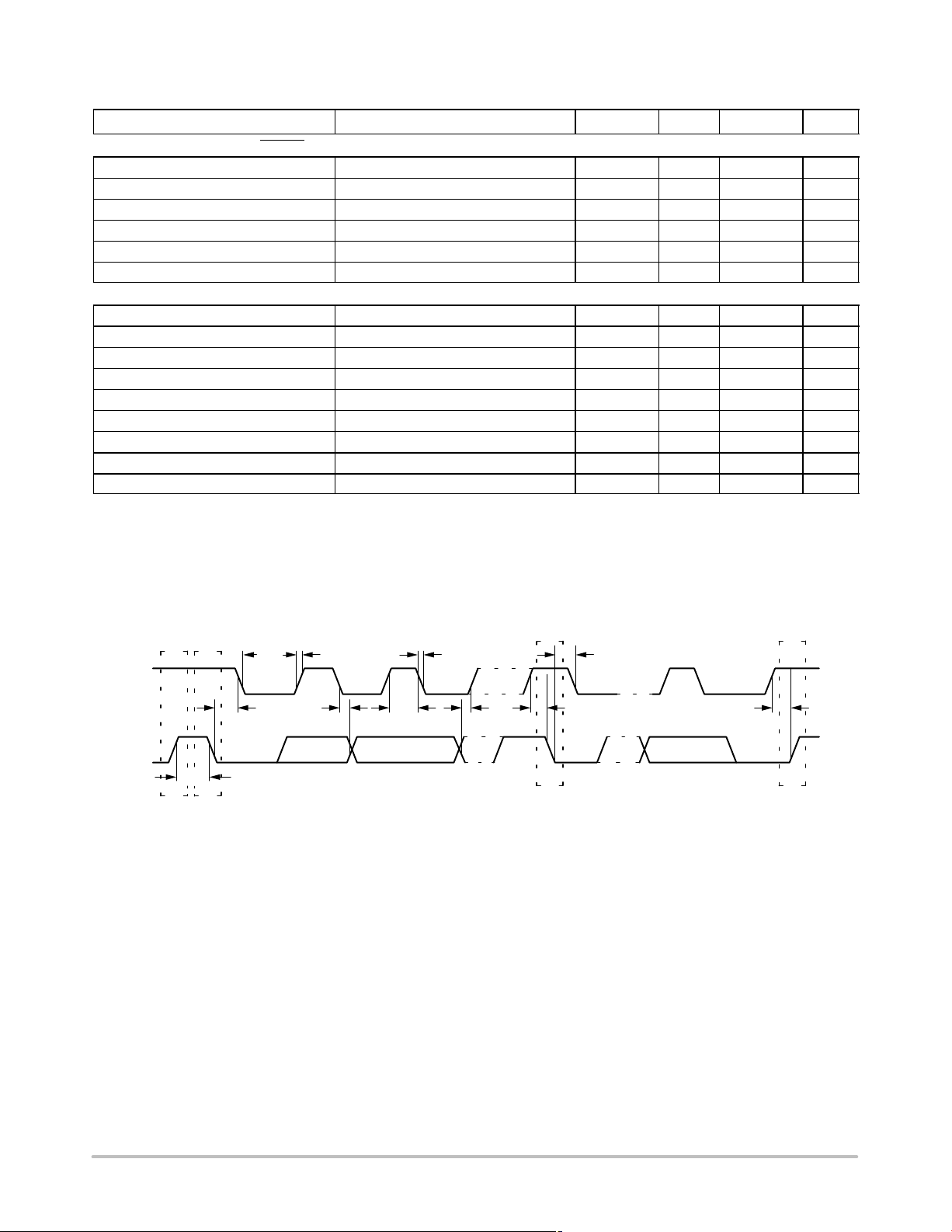
Serial Bus Timing (Note 2) (See Figure 2)
Clock Frequency, f
Glitch Immunity, t
Bus Free Time, t
SCL Low Time, t
SCL High Time, t
SCL, SDA Rise Time, t
SCL, SDA Fall Time, t
Data Setup Time, t
SCLK
SW
BUF
LOW
HIGH
r
f
SU; DAT
Detect Clock Low Timeout, t
TIMEOUT
Can be optionally disabled 15 35 ms
10 400 kHz
50 ns
4.7
4.7
4.0 50
ms
ms
ms
1,000 ns
300
ms
250 ns
1. All voltages are measured with respect to GND, unless otherwise noted. Typicals are at TA = 25°C and represent most likely parametric norm.
Logic inputs accept input high voltages up to V
levels of V
2. Serial management bus (SMBus) timing specifications are guaranteed by design and are not production tested.
= 0.8 V for a falling edge and VIH = 2.0 V for a rising edge.
IL
, even when the device is operating down to V
MAX
. Timing specifications are tested at logic
MIN
SCL
SDA
t
BUF
PS
t
HD: STA
t
LOW
t
HIGH
t
F
t
SU: DAT
t
HD: STA
t
SU: STA
SP
t
SU: STO
t
R
t
HD: DAT
Figure 2. Serial Bus Timing Diagram
http://onsemi.com
4
Page 5
ADT7473
PIN ASSIGNMENT
Pin No. Mnemonic Description
1 SCL Digital Input (Open Drain). SMBus serial clock input. Requires SMBus pullup.
2 GND Ground Pin.
3 V
4 TACH3 Digital Input (Open Drain). Fan tachometer input to measure speed of Fan 3.
5 PWM2
6 TACH1 Digital Input (Open Drain). Fan tachometer input to measure speed of Fan 1.
7 TACH2 Digital Input (Open Drain). Fan tachometer input to measure speed of Fan 2.
8 PWM3 Digital I/O (Open Drain). Pulse−width modulated output to control the speed of Fan 3 and Fan 4.
9 TACH4 Digital Input (Open Drain). Fan tachometer input to measure speed of Fan 4.
10 D2− Cathode Connection to Second Thermal Diode.
11 D2+ Anode Connection to Second Thermal Diode.
12 D1− Cathode Connection to First Thermal Diode.
13 D1+ Anode Connection to First Thermal Diode.
14 V
15 PWM1
16 SDA
CC
ADDR SELECT If in address select mode, the logic state of this pin defines the SMBus device address.
SMBALERT On the ADT7473, this pin can be reconfigured as an SMBALERT interrupt output to signal out−of−limit
THERM_LATCH ADT7473−1 default pin function. THERM_LATCH is a thermal event alert signal when an
ADDREN If pulled low on powerup, the ADT7473−1 enters address select mode, and the state of Pin 4
GPIO General Purpose Open Drain Digital I/O.
THERM Bidirectional THERM pin. Can be used to time and monitor assertions on the THERM input as well as
SMBALERT Digital Output (Open Drain). This pin can be reconfigured as an SMBALERT interrupt output to signal
CCP
XTO
Power Supply. Powered by 3.3 V.
Digital Output (Open Drain). ADT7473 default pin function is PWM2. Requires 10 kW typical pullup.
Pulse−width modulated output to control Fan 2 speed. Can be configured as a high or low frequency
drive.
conditions.
overtemperature condition occurs.
Requires 10 kW typical pullup. Can be configured as a high or low frequency drive.
(ADDR SELECT
to assert when an ADT7473 THERM
connected to the PROCHOT output of an IntelR PentiumR 4 processor or to the output of a trip point
temperature sensor. Can be used as an output to signal overtemperature conditions.
out−of−limit conditions.
Analog Input. Monitors processor core voltage (0 V to 3.0 V).
Digital Output (Open Drain). Pulse−width modulated output to control Fan 1 speed. Requires 10 kW
typical pullup.
Also functions as the output from the XNOR tree in XNOR test mode.
Digital I/O (Open Drain). SMBus bidirectional serial data. Requires 10 kW typical pullup.
) determines the ADT7473−1 slave address.
overtemperature limit is exceeded. For example, the pin can be
http://onsemi.com
5
Page 6
ADT7473
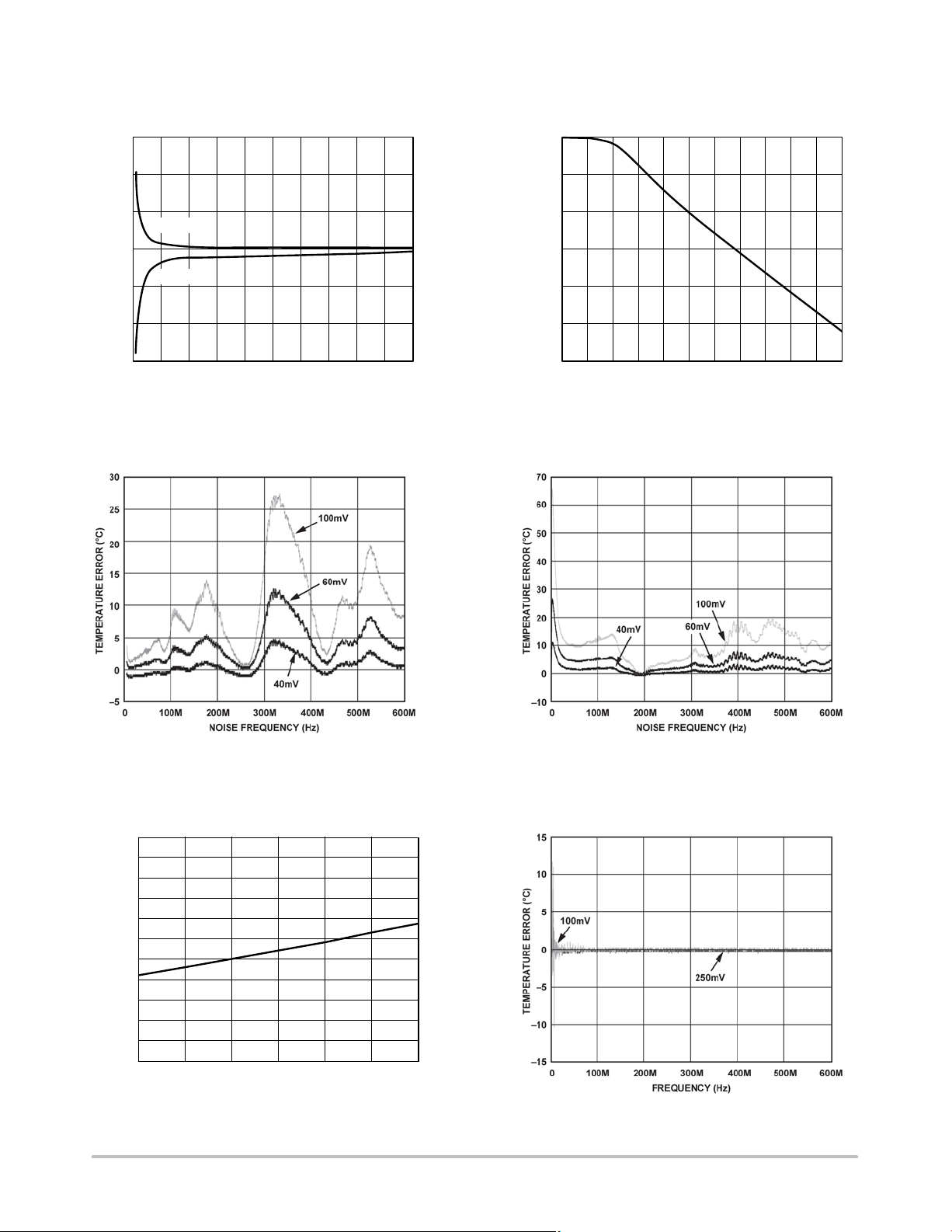
TYPICAL CHARACTERISTICS
60
40
20
D+ TO GND
0
D+ TO V
–20
TEMPERATURE ERROR (5C)
–40
–60
0204060
CC
80 10010 30 50 70 90
LEAKAGE RESISTANCE (MΩ)
Figure 3. Remote Temperature Error vs. PCB
Resistance
0
–10
–20
–30
–40
TEMPERATURE ERROR (5C)
–50
–60
0 2 4 6 8 10 12
CAPACITANCE (nF)
14 16 18 20 22
Figure 4. Temperature Error vs. Capacitance
Between D+ and D−
Figure 5. Remote Temperature Error vs.
Common−Mode Noise Frequency
1.20
1.18
1.16
1.14
1.12
1.10
(mA)
1.08
DD
I
1.06
1.04
1.02
1.00
0.98
3.0 3.1 3.2 3.3 3.4
Figure 7. Normal I
(V)
V
DD
vs. Power Supply Figure 8. Internal Temperature Error vs.
DD
Figure 6. Remote Temperature Error vs.
Common−Mode Noise Frequency
3.5 3.6
Frequency
http://onsemi.com
6
Page 7
ADT7473
TYPICAL CHARACTERISTICS
3.0
2.5
2.0
1.5
1.0
0.5
0
–0.5
TEMPERATURE ERROR (5C)
–1.0
–1.5
–2.0
–40 –20 0 20 40 60 85
OIL BATH TEMPERATURE (5C)
105 125
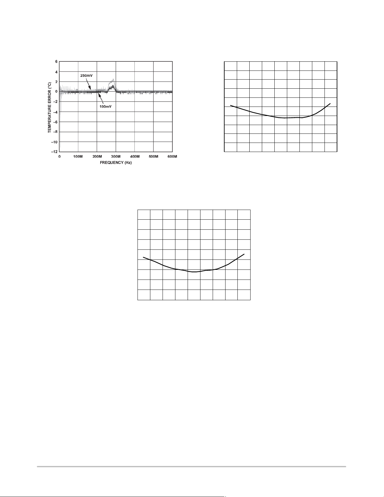
Figure 9. Remote Temperature Error vs. Power
Supply Noise Frequency
3.0
2.5
2.0
1.5
1.0
0.5
0
TEMPERATURE ERROR (5C)
0.5
1.0
1.5
–40 –20 0 20 40 60 85
OIL BATH TEMPERATURE (5C)
Figure 11. Remote Temperature Error vs. Temperature
Figure 10. Internal Temperature Error vs.
Temperature
105 125
http://onsemi.com
7
Page 8

ADT7473
Product Description
The ADT7473/ADT7473−1 is a complete thermal
monitor and multiple fan controller for any system requiring
thermal monitoring and cooling. The device communicates
with the system via a serial system management bus. The
serial bus controller has a serial data line for reading and
writing addresses and data (Pin 16), and an input line for the
serial clock (Pin 1). All control and programming functions
for the ADT7473/ADT7473−1 are performed over the serial
bus. Additionally, a pin can be reconfigured as an
SMBALERT
output to signal out−of−limit conditions.
Table 1 illustrates the differences between the ADT7473
and the ADT7473−1.
Table 1. ADT7473/ADT7473−1 Device Comparison
Feature ADT7473 ADT7473−1
Pin 5 Default:
SMBus Address Fixed
Remote Ch. 2
Therm Limit
Register 0x30,
0x31, 0x32
Register 0x3F
Revision Reg
Register 0x40, Bit 7 Reserved (R/W) 1 = Reset Latch
Register 0x42, Bit 0 Reserved (Read−only)
Registers 0x5C,
0x5D, 0x5E
Register 0x7C, Bit 4 Reserved THERM Output
Register 0x7D, Bit 4 Reserved
Comparison Between ADT7467 and
ADT7473/ADT7473−1
PWM2
Address
= 100°C = 136°C
Default:
0x00
Default:
0x68
Default:
0x82
Default:
THERM_LATCH
Address selectable
Default: 0xFF
Default: 0x69
(lockable)
1 = THERM
Limit Latched
Default: 0x62
Hysteresis
THERM_LATCH
Configuration
0 = Remote Channel 2
1 = Remote Channel 1
and Remote Channel 2
The following list shows some comparisons between the
ADT7467 and the ADT7473/ADT7473−1:
• The ADT7473/ADT7473−1 can be powered via a
3.3 V supply only, and does not support 5.0 V
operation, while the ADT7467 does. Violating this
specification results in irreversible damage to the
ADT7473/ADT7473−1. See the Specifications section
for more information.
• A high frequency PWM drive can be independently
selected for each PWM channel on the
ADT7473/ADT7473−1. This is not available on the
ADT7467.
• The range and resolution of the temperature offset
register can be changed from a ±64°C range at 0.5°C
resolution to a ±128°C range at 1°C resolution. This is
not available on the ADT7467.
• THERM overtemperature events can be
disabled/enabled individually on each temperature
channel. This is not available on the ADT7467.
• Bit 7 of Configuration Register 1 is no longer supported
because the ADT7473/ADT7473−1 cannot be powered
via a 5.0 V supply.
• Bit 0 of Configuration Register 1 (0x40) remains
writable after the lock bit is set. This bit enables
monitoring.
• 2−wire fan speed measurement is not supported on the
ADT7473/ADT7473−1.
How to Set the Functionality of Pin 9
Pin 9 on the ADT7473/ADT7473−1 has four possible
functions: SMBALERT
, THERM, GPIO, and TACH4. The
user chooses the required functionality by setting Bit 0 and
Bit 1 of Configuration Register 4 (0x7D).
Table 2. Pin 9 Settings
Bit 0 Bit 1 Function
0 0 TACH4
0 1 THERM
1 0 SMBALERT
1 1 GPIO
Recommended Implementation
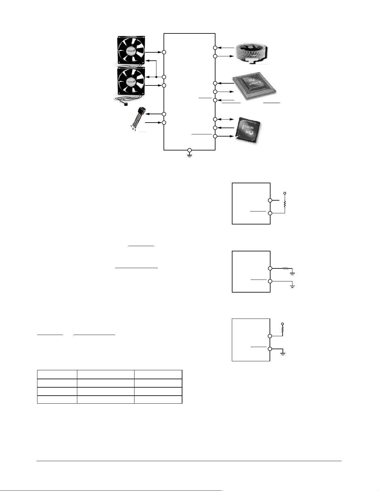
Configuring the ADT7473 as shown in Figure 12 allows
the system designer to use the following features:
• Two PWM outputs for fan control of up to three fans.
(The front and rear chassis fans are connected in
parallel.)
• Three TACH fan speed measurement inputs.
• V
measured internally through Pin 3.
CC
• CPU temperature measured using Remote 1
temperature channel.
• Ambient temperature measured through Remote 2
temperature channel.
• Bidirectional THERM pin. This feature allows Intel
Pentium 4 PROCHOT
an overtemperature THERM
be programmed as an SMBALERT
output.
monitoring and can function as
output. It can alternatively
system interrupt
http://onsemi.com
8
Page 9
ADT7473
FRONT
CHASSIS
FAN
REAR
CHASSIS
FAN
AMBIENT
TEMPERATURE
TACH2
PWM3
TACH3
D1+
D1–
Figure 12. ADT7473 Configuration
Serial Bus Interface
On PCs and servers, control of the ADT7473/ADT7473−1
is carried out using the SMBus. The ADT7473/ADT7473−1
is connected to this bus as a slave device, under the control of
a master controller, which is usually (but not necessarily) the
ICH.
The ADT7473 has a fixed 7−bit serial bus address of
0101110 or 0x2E. The read/write bit must be added to get the
8−bit address (01011100 or 0x5C). When the ADT7473−1
is powered up with Pin 8 (PWM3/ADDREN
) high, the
ADT7473−1 has a default SMBus address of 0101110 or
0x2E. If more than one ADT7473−1 is used in a system,
each ADT7473−1 is placed in ADDR SELECT
mode by
strapping Pin 8 low on powerup. The logic state of Pin 4 then
determines the device’s SMBus address. The logic of these
pins is sampled on powerup.
The device address is sampled on powerup and latched on
the first valid SMBus transaction, more precisely on the
low−to−high transition at the beginning of the eighth SCL
pulse, when the serial bus address byte matches the selected
slave address. The selected slave address is chosen using the
ADDREN
pin/ADDR SELECT pin. Any attempted change
in the address has no effect after this.
Table 3. Hardwiring the ADT7473−1 SMBus Device
Address
Pin 13 State Pin 14 State Address
0
0
Low (10 kW to GND)
High (10 kW pullup)
1 Don’t care 0101110 (0x2E)
0101100 (0x2C)
0101101 (0x2D)
ADT7473
SMBALERT
GND
CPU FAN
PWM1
TACH1
D2+
D2–
THERM
SDA
SCL
PROCHOT
ADT7473−1
ADDR SELECT
PWM3/ADDREN
ICH
CPU
4
8
ADDRESS = 0x2E
V
CC
10kΩ
Figure 13. Default SMBus Address = 0x2E
ADT7473−1
10kΩ
ADDR SELECT
PWM3/ADDREN
4
8
ADDRESS = 0x2C
Figure 14. SMBus Address = 0x2C (Pin4 = 0)
V
ADT7473−1
ADDR SELECT
PWM3/ADDREN
CC
10kΩ
4
8
ADDRESS = 0x2D
Figure 15. SMBus Address = 0x2D (Pin 4 = 1)
http://onsemi.com
9
Page 10
ADT7473
V
ADT7473−1
ADDR SELECT
PWM3/ADDREN
CARE SHOULD BE TAKEN TO ENSURE THAT PIN 8
(PWM3/ADDREN) IS EITHER TIED HIGH OR LOW. LEAVING PIN 8
FLOATING COULD CAUSE THE ADT7473-1 TO POWER UP WITH
AN UNEXPECTED ADDRESS.
NOTE THAT IF THE ADT7473-1 IS PLACED INTO ADDR SELECT
MODE, PINS 8 AND 4 CANNOT BE USED AS THE ALTERNATIVE
FUNCTIONS (PWM3, TACH4/THERM) UNLESS THE CORRECT
CIRCUIT IS MUXED IN AT THE CORRECT TIME OR DESIGNED TO
HANDLE THESE DUAL FUNCTIONS.
CC
10kΩ
4
8
NC
DO NOT LEAVE ADDREN
UNCONNECTED! CAN
CAUSE UNPREDICTABLE
ADDRESSES.
Figure 16. Unpredictable SMBus Address if Pin 8
is Unconnected
The ability to make hardwired changes to the SMBus
slave address allows the user to avoid conflicts with other
devices sharing the same serial bus, for example, if more
than one ADT7473−1 is used in a system.
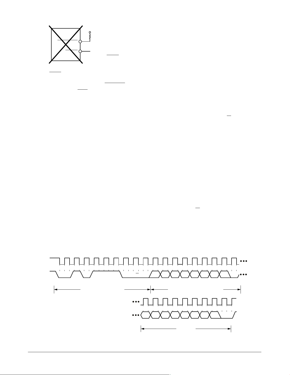
Data is sent over the serial bus in sequences of nine clock
pulses: eight bits of data followed by an acknowledge bit
from the slave device. Transitions on the data line must
occur during the low period of the clock signal and remain
stable during the high period because a low−to−high
transition when the clock is high might be interpreted as a
stop signal. The number of data bytes that can be transmitted
over the serial bus in a single read or write operation is
limited only by what the master and slave devices can
handle.
When all data bytes have been read or written, stop
conditions are established. In write mode, the master pulls
the data line high during the tenth clock pulse to assert a stop
condition. In read mode, the master device overrides the
acknowledge bit by pulling the data line high during the low
period before the ninth clock pulse; this is known as No
Acknowledge. The master takes the data line low during the
low period before the tenth clock pulse, and then high during
the tenth clock pulse to assert a stop condition.
Any number of bytes of data can be transferred over the
serial bus in one operation, but it is not possible to mix read
and write in one operation, because the type of operation is
determined at the beginning and cannot subsequently be
changed without starting a new operation.
In the ADT7473/ADT7473−1, write operations contain
either one or two bytes, and read operations contain one
byte. To write data to one of the device data registers or read
data from it, the address pointer register must be set so the
correct data register is addressed, and then data can be
written into that register or read from it. The first byte of a
write operation always contains an address that is stored in
the address pointer register. If data is written to the device,
the write operation contains a second data byte that is written
to the register selected by the address pointer register.
This write operation is shown in Figure 17. The device
address is sent over the bus, and then R/W
is set to 0. This
is followed by two data bytes. The first data byte is the
address of the internal data register to be written to, which
is stored in the address pointer register. The second data byte
is the data to be written to the internal data register.
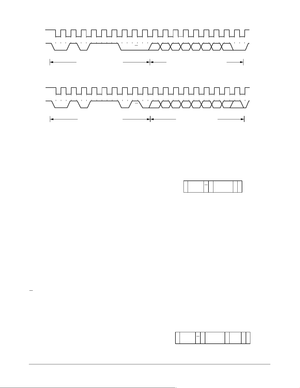
When reading data from a register, there are two
possibilities:
• If the ADT7473/ADT7473−1’s address pointer register
value is unknown or not the desired value, it must first
be set to the correct value before data can be read from
the desired data register. This is done by performing a
write to the ADT7473/ADT7473−1, but only the data
byte containing the register address is sent, because no
data is written to the register. This is shown in
Figure 18.
A read operation is then performed consisting of the
serial bus address, R/W
bit set to 1, followed by the
data byte read from the data register. This is shown in
Figure 19.
• If the address pointer register is known to be already at
the desired address, data can be read from the
corresponding data register without first writing to the
address pointer register, as shown in Figure 19.
D0
9
ACK. BY
9
ACK. BY
STOP BY
MASTER
SCL
SDA
START BY
MASTER
19
0
1011
FRAME 1
SERIAL BUS ADDRESS BYTE
SCL (CONTINUED)
SDA (CONTINUED)
0
1
R/W
ACK. BY
ADT7473/ADT7473−1
1
D6
D7
1
D7
D5
D6
D4
D5
ADDRESS POINTER REGISTER BYTE
D4
D3
FRAME 3
DATA BYTE
D3
FRAME 2
D2
D2
D1
ADT7473/ADT7473−1
D1
D0
ADT7473/ADT7473−1
Figure 17. Writing a Register Address to the Address Pointer Register, then Writing Data to the Selected Register
http://onsemi.com
10
Page 11
ADT7473
1
SCL
SDA
START BY
MASTER
0
1011
SERIAL BUS ADDRESS BYTE
FRAME 1
0
1
R/W
ACK. BY
ADT7473/ADT7473−1
Figure 18. Writing to the Address Pointer Register Only
1
SCL
0
SDA
START BY
MASTER
10
SERIAL BUS ADDRESS BYTE
1
FRAME 1
1
0
1
R/W
ACK. BY
ADT7473/ADT7473−1
Figure 19. Reading Data from a Previously Selected Register
It is possible to read a data byte from a data register
without first writing to the address pointer register, if the
address pointer register is already at the correct value.
However, it is not possible to write data to a register without
writing to the address pointer register, because the first data
byte of a write is always written to the address pointer
register.
In addition to supporting the send byte and receive byte
protocols, the ADT7473/ADT7473−1 also supports the read
byte protocol. (See System Management Bus (SMBus)
Specifications Version 2 for more information; this
document is available from Intel.)
If several read or write operations must be performed in
succession, the master can send a repeat start condition
instead of a stop condition to begin a new operation.
Write Operations
The SMBus specification defines several protocols for
various read and write operations. The ADT7473/
ADT7473−1 uses the following SMBus write protocols. The
following abbreviations are used in the diagrams:
S—Start
P—Stop
R—Read
W—Write
A—Acknowledge
A
—No Acknowledge
Send Byte
In this operation, the master device sends a single
command byte to a slave device, as follows:
1. The master device asserts a start condition on
SDA.
2. The master sends the 7−bit slave address followed
by the write bit (active low).
3. The addressed slave device asserts ACK on SDA.
4. The master sends a command code.
5. The slave asserts ACK on SDA.
19
D6
D7
19
D6
D7
D4
D5
ADDRESS POINTER REGISTER BYTE
D4
D5
DATA BYTE FROM ADT7473
D3
FRAME 2
D3
FRAME 2
D2
D1
ADT7473/ADT7473−1
D2
D1
9
D0
ACK. BY
D0
NO ACK. BY
MASTER
STOP BY
MASTER
9
STOP BY
MASTER
6. The master asserts a stop condition on SDA and
the transaction ends.
For the ADT7473/ADT7473−1, the send byte protocol is
used to write a register address to RAM for a subsequent
single−byte read from the same address. This operation is
illustrated in Figure 20.
231564
SLAVE
ADDRESS
REGISTER
WASAP
ADDRESS
Figure 20. Setting a Register Address for
Subsequent Read
If the master is required to read data from the register
immediately after setting up the address, it can assert a repeat
start condition immediately after the final ACK and carry
out a single−byte read without asserting an intermediate stop
condition.
Write Byte
In this operation, the master device sends a command byte
and one data byte to the slave device, as follows:
1. The master device asserts a start condition on SDA.
2. The master sends the 7−bit slave address followed
by the write bit (active low).
3. The addressed slave device asserts ACK on SDA.
4. The master sends a command code.
5. The slave asserts ACK on SDA.
6. The master sends a data byte.
7. The slave asserts ACK on SDA.
8. The master asserts a stop condition on SDA, and
the transaction ends.
The single byte write operation is illustrated in Figure 21.
23156784
SLAVE
ADDRESS
Figure 21. Single−Byte Write to a Register
REGISTER
W A DATASAAP
ADDRESS
http://onsemi.com
11
Page 12
ADT7473
Read Operations
The ADT7473/ADT7473−1 uses the following SMBus
read protocols.
Receive Byte
This operation is useful when repeatedly reading a single
register. The register address must have been previously set
up. In this operation, the master device receives a single byte
from a slave device, as follows:
1. The master device asserts a start condition on
SDA.
2. The master sends the 7−bit slave address followed
by the read bit (high).
3. The addressed slave device asserts ACK on SDA.
4. The master receives a data byte.
5. The master asserts NO ACK on SDA.
6. The master asserts a stop condition on SDA, and
the transaction ends.
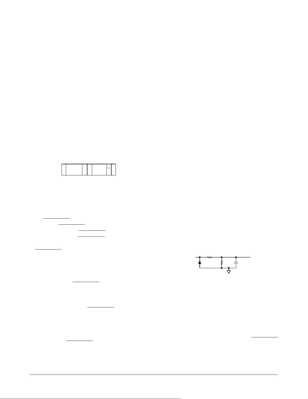
In the ADT7473/ADT7473−1, the receive byte protocol
is used to read a single byte of data from a register whose
address has previously been set by a send byte or write byte
operation. This operation is illustrated in Figure 22.
243156
SLAVE
ADDRESS
Figure 22. Single−Byte Read from a Register
Alert Response Address
DATAARSAP
Alert response address (ARA) is a feature of SMBus
devices that allows an interrupting device to identify itself
to the host when multiple devices exist on the same bus.
The SMBALERT
output or an SMBALERT
connected to a common SMBALERT
master. If a device’s SMBALERT
output can be used as either an interrupt
. One or more outputs can be
line connected to the
line goes low, the
following events occur:
• SMBALERT is pulled low.
• The master initiates a read operation and sends the alert
response address (ARA = 0001 100). This is a general
call address that must not be used as a specific device
address.
• The device whose SMBALERT output is low responds
to the alert response address, and the master reads its
device address. The address of the device is now known
and can be interrogated in the usual way.
• If more than one device’s SMBALERT output is low,
the one with the lowest device address has priority in
accordance with normal SMBus arbitration.
Once the ADT7473/ADT7473−1 has responded to the
alert response address, the master must read the status
registers, and the SMBALERT
condition is gone.
is cleared only if the error
SMBus Timeout
The ADT7473/ADT7473−1 includes an SMBus timeout
feature. If there is no SMBus activity for 35 ms, the
ADT7473/ADT7473−1 assumes the bus is locked and
releases the bus. This prevents the device from locking or
holding the SMBus expecting data. Some SMBus
controllers cannot work with the SMBus timeout feature, so
it can be disabled.
Configuration Register 1 (0x40)
Bit 6, TODIS = 0; SMBus timeout enabled (default)
Bit 6, TODIS = 1; SMBus timeout disabled
Voltage Measurement Input
The ADT7473/ADT7473−1 has one external voltage
measurement channel and can also measure its own supply
voltage, VCC. Pin 14 can measure VCCP. The VCC supply
voltage measurement is carried out through the VCC pin
(Pin 3). The VCCP input can be used to monitor a chipset
supply voltage in computer systems.
Analog−to−Digital Converter
All analog inputs are multiplexed into the on−chip,
successive approximation, analog−to−digital converter.
(ADC) This has a resolution of 10 bits. The basic input range
is 0 V to 2.25 V, but the input has built−in attenuators to allow
measurement of V
without any external components. To
CCP
allow for the tolerance of the supply voltage, the ADC
produces an output of 3/4 full scale (768 decimal or 300
hexadecimal) for the nominal input voltage and thus has
adequate headroom to deal with overvoltages.
Input Circuitry
The internal structure for the V
analog input is shown
CCP
in Figure 23. The input circuit consists of an input protection
diode, an attenuator, plus a capacitor to form a first order
low−pass filter that provides the input immunity to high
frequency noise.
V
CCP
Figure 23. Structure of Analog Inputs
Voltage Measurement Registers
Register 0x21, V
17.5kΩ
52.5kΩ
Reading = 0x00 default
CCP
35pF
Register 0x22, VCC Reading = 0x00 default
V
Limit Registers
CCP
Associated with the V
measurement channel is a high
CCP
and low limit register. Exceeding the programmed high or
low limit causes the appropriate status bit to be set.
Exceeding either limit can also generate SMBALERT
interrupts.
Register 0x46, V
Register 0x47, V
Low Limit = 0x00 default
CCP
High Limit = 0xFF default
CCP
http://onsemi.com
12
Page 13

ADT7473
Table 5 shows the input ranges of the analog inputs and
output codes of the 10−bit ADC.
When the ADC is running, it samples and converts a
voltage input in 711 ms and averages 16 conversions to
reduce noise; a measurement takes nominally 11.38 ms.
Additional ADC Functions for Voltage Measurements
A number of other functions are available on the
ADT7473/ADT7473−1 to offer the system designer
increased flexibility.
Turn−Off Averaging
For each voltage measurement read from a value register,
16 readings have actually been made internally and the
results averaged before being placed into the value register.
When faster conversions are needed, setting Bit 4 of
Configuration Register 2 (0x73) turns averaging off. This
effectively gives a reading 16 times faster (711 ms), but the
reading may be noisier.
Bypass Voltage Input Attenuator
Setting Bit 5 of Configuration Register 2 (0x73) removes
the attenuation circuitry from the V
input. This allows
CCP
the user to directly connect external sensors or to rescale the
analog voltage measurement inputs for other applications.
The input range of the ADC without the attenuators is 0 V
to 2.25 V.
Single−Channel ADC Conversion
Setting Bit 6 of Configuration Register 2 (0x73) places the
ADT7473/ADT7473−1 into single−channel ADC
conversion mode. In this mode, the ADT7473/ADT7473−1
can be made to read a single voltage channel only. If the
internal ADT7473/ADT7473−1 clock is used, the selected
input is read every 711 ms. The appropriate ADC channel is
selected by writing to Bits [7:5] of the TACH1 minimum
high byte register (0x55).
Table 4. Programming Single−Channel ADC Mode
Bits [7:5], Register 0x55 Channel Selected
001 V
010 V
101 Remote 1 temperature
110 Local temperature
111 Remote 2 temperature
Configuration Register 2 (0x73)
CCP
CC
Bit 4 = 1; averaging off.
Bit 5 = 1; bypass input attenuators.
Bit 6 = 1; single−channel convert mode.
TACH1 Minimum High Byte Register (0x55)
Bits [7:5] select ADC channel for single−channel convert
mode.
http://onsemi.com
13
Page 14

ADT7473
Table 5. 10−Bit ADC Output Code vs. V
VCC (3.3 VIN) (Note 3) V
<0.0042 <0.00293 0 00000000 00
0.0042 to 0.0085 0.0293 to 0.0058 1 00000000 01
0.0085 to 0.0128 0.0058 to 0.0087 2 00000000 10
0.0128 to 0.0171 0.0087 to 0.0117 3 00000000 11
0.0171 to 0.0214 0.0117 to 0.0146 4 00000001 00
0.0214 to 0.0257 0.0146 to 0.0175 5 00000001 01
0.0257 to 0.0300 0.0175 to 0.0205 6 00000001 10
0.0300 to 0.0343 0.0205 to 0.0234 7 00000001 11
0.0343 to 0.0386 0.0234 to 0.0263 8 00000010 00
− − − −
1.100 to 1.1042 0.7500 to 0.7529 256 (1/4 scale) 01000000 00
− − − −
2.200 to 2.2042 1.5000 to 1.5029 512 (1/2 scale) 10000000 00
− − − −
3.300 to 3.3042 2.2500 to 2.2529 768 (3/4 scale) 11000000 00
− − − −
4.3527 to 4.3570 2.9677 to 2.9707 1013 11111101 01
4.3570 to 4.3613 2.9707 to 2.9736 1014 11111101 10
4.3613 to 4.3656 2.9736 to 2.9765 1015 11111101 11
4.3656 to 4.3699 2.9765 to 2.9794 1016 11111110 00
4.3699 to 4.3742 2.9794 to 2.9824 1017 11111110 01
4.3742 to 4.3785 2.9824 to 2.9853 1018 11111110 10
4.3785 to 4.3828 2.9853 to 2.9882 1019 11111110 11
4.3828 to 4.3871 2.9882 to 2.9912 1020 11111111 0 0
4.3871 to 4.3914 2.9912 to 2.9941 1021 11111111 0 1
4.3914 to 4.3957 2.9941 to 2.9970 1022 11111111 1 0
>4.3957 >2.9970 1023 11111111 11
3. The VCC output codes listed assume that VCC is 3.3 V.
IN
CCP
ADC Output
Decimal Binary (10 Bits)
Temperature Measurement Method
A simple method of measuring temperature is to exploit
the negative temperature coefficient of a diode, measuring
the base−emitter voltage (VBE) of a transistor operated at
constant current. Unfortunately, this technique requires
calibration to null out the effect of the absolute value of
VBE, which varies from device to device.
The technique used in the ADT7473/ADT7473−1
measures the change in VBE when the device is operated at
three different currents. Previous devices have used only
two operating currents, but the use of a third current allows
automatic cancellation of resistances in series with the
external temperature sensor.
http://onsemi.com
Figure 24 shows the input signal conditioning used to
measure the output of an external temperature sensor. This
figure shows the external sensor as a substrate transistor, but
it could equally be a discrete transistor. If a discrete
transistor is used, the collector is not grounded and should
be linked to the base. To prevent ground noise from
interfering with the measurement, the more negative
terminal of the sensor is not referenced to ground, but is
biased above ground by an internal diode at the D− input. C1
can optionally be added as a noise filter (recommended
maximum value 1000 pF). However, a better option in noisy
environments is to add a filter, as described in the Noise
Filtering section.
14
Page 15

ADT7473
Local Temperature Measurement
The ADT7473/ADT7473−1 contains an on−chip band
gap temperature sensor whose output is digitized by the
on−chip 10−bit ADC. The 8−bit MSB temperature data is
stored in the local temperature register (0x26). Because both
positive and negative temperatures can be measured, the
temperature data is stored in Offset 64 format or twos
complement format, as shown in Table 10 and Table 11.
Theoretically, the temperature sensor and ADC can measure
temperatures from −63°C to +127°C (or −63°C to +191°C in
the extended temperature range) with a resolution of
+0.25°C. However, this exceeds the operating temperature
range of the device, so local temperature measurements
outside the ADT7473/ADT7473−1 operating temperature
range are not possible.
Table 6. Twos Complement Temperature Data Format
Temperature Digital Output (10−Bit) (Note 1)
–128°C 1000 0000 00 (diode fault)
–63°C 1100 0001 00
–50°C 1100 1110 00
–25°C 1110 0111 00
–10°C 1111 0 11 0 00
0°C 0000 0000 00
10.25°C 0000 1010 01
25.5°C 0001 1001 10
50.75°C 0011 0010 11
75°C 0100 1011 00
100°C 0110 0100 00
125°C 0111 1101 00
127°C 0111 1111 00
1. Bold numbers denote 2 LSBs of measurement in the Extended
Resolution Register 2 (Register 0x77) with 0.25°C resolution.
Remote Temperature Measurement
The ADT7473/ADT7473−1 can measure the temperature
of two remote diode sensors or diode−connected transistors
connected to Pin 10 and Pin 11 or to Pin 12 and Pin 13.
The forward voltage of a diode or diode−connected
transistor operated at a constant current exhibits a negative
temperature coefficient of about −2 mV/°C. Unfortunately,
the absolute value of V
varies from device to device and
BE
individual calibration is required to null this out, so the
technique is unsuitable for mass production. The technique
used in the ADT7473/ADT7473−1 is to measure the change
in V
when the device is operated at three different
BE
currents. This is given by:
DV
= kT/q x ln(N)
BE
where:
k is Boltzmann’s constant.
T is the absolute temperature in Kelvin.
q is the charge on the carrier.
N is the ratio of the two currents.
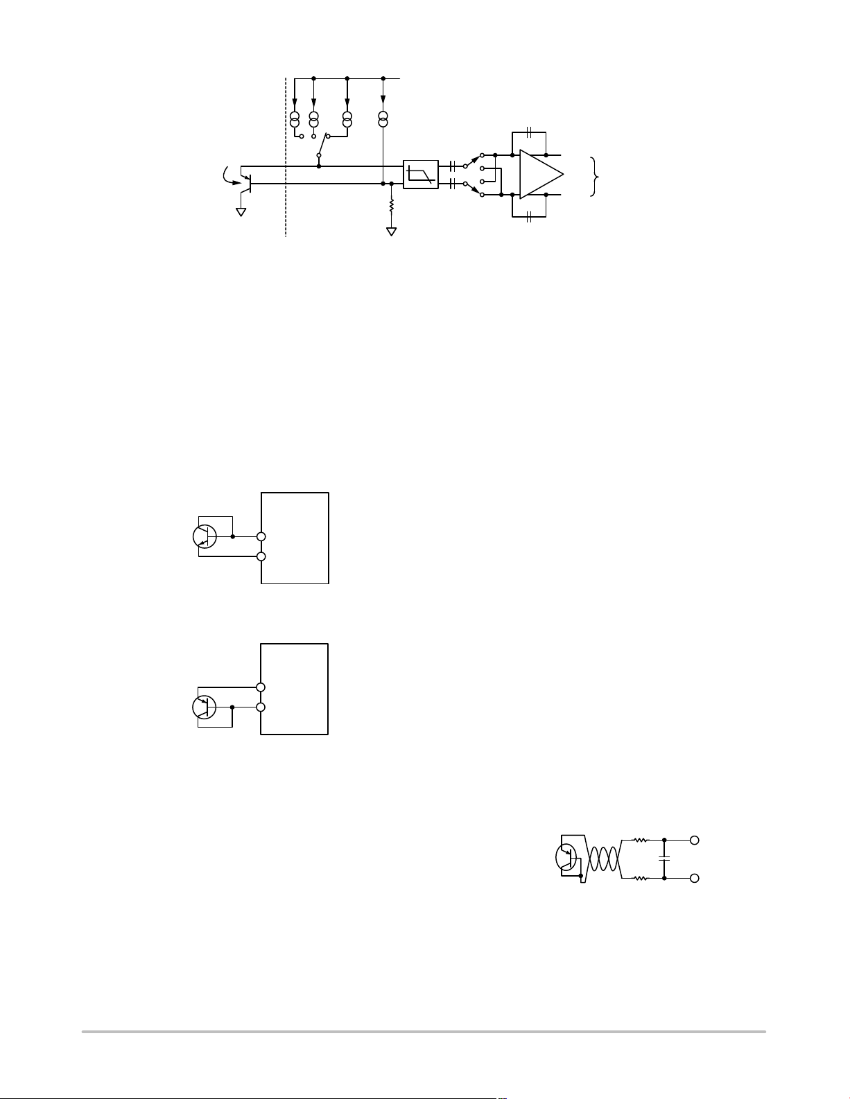
Figure 24 shows the input signal conditioning used to
measure the output of a remote temperature sensor. This
figure shows the external sensor as a substrate transistor,
provided for temperature monitoring on some micro−
processors. It could also be a discrete transistor such as a
2N3904/2N3906.
Table 7. Extended Range, Temperature Data Format
Temperature Digital Output (10−Bit) (Note 1)
–64°C 0000 0000 00 (diode fault)
–63°C 0000 0001 00
–1°C 0011 1111 00
0°C 0100 0000 00
1°C 0100 0001 00
10°C 0100 1010 00
25°C 0101 1001 00
50°C 0111 0010 00
75°C 1000 1001 00
100°C 1010 0100 00
125°C 1011 1101 00
191°C 1111 1111 00
1. Bold numbers denote 2 LSBs of measurement in the Extended
Resolution Register 2 (Register 0x77) with 0.25°C resolution.
http://onsemi.com
15
Page 16
ADT7473
V
DD
I
I N1 y IN2 y I
REMOTE
SENSING
TRANSISTOR
D+
D–
Figure 24. Signal Conditioning for Remote Diode Temperature Sensors
BIAS
LPF
f
= 65kHz
C
V
V
OUT+
TO ADC
OUT–
If a discrete transistor is used, the collector is not grounded
and should be linked to the base. If a PNP transistor is used,
the base is connected to the D– input and the emitter is
connected to the D+ input. If an NPN transistor is used, the
emitter is connected to the D– input and the base is
connected to the D+ input. Figure 25 and Figure 26 show
how to connect the ADT7473/ADT7473−1 to an NPN or
PNP transistor for temperature measurement. To prevent
ground noise from interfering with the measurement, the
more negative terminal of the sensor is not referenced to
ground, but is biased above ground by an internal diode at
the D– input.
ADT7473/
ADT7473−1
2N3904
NPN
D+
D–
Figure 25. Measuring Temperature Using an NPN
Transistor
ADT7473/
ADT7473−1
D+
2N3906
PNP
D–
Figure 26. Measuring Temperature Using a PNP
Transistor
To measure DVBE, the operating current through the
sensor is switched among three related currents. N1 x I and
N2 x I are different multiples of the current I, as shown in
Figure 24. The currents through the temperature diode are
switched between I and N1 x I, giving DV
between I and N2 x I, giving DV
then be calculated using the two DV
. The temperature can
BE2
measurements. This
BE
, and then
BE1
method can also cancel the effect of any series resistance on
the temperature measurement.
The resulting DVBE waveforms are passed through a
65 kHz low−pass filter to remove noise and then to a
chopper−stabilized amplifier. This amplifies and rectifies
the waveform to produce a dc voltage proportional to DVBE.
The ADC digitizes this voltage, and a temperature
measurement is produced. To reduce the effects of noise,
digital filtering is performed by averaging the results of 16
measurement cycles.
The results of remote temperature measurements are
stored in 10−bit, twos complement format, as listed in Table
10. The extra resolution for the temperature measurements
is held in the Extended Resolution Register 2 (0x77). This
gives temperature readings with a resolution of 0.25°C.
Noise Filtering
For temperature sensors operating in noisy environments,
previous practice was to place a capacitor across the D+ pin
and the D− pin to help combat the effects of noise. However,
large capacitances affect the accuracy of the temperature
measurement, leading to a recommended maximum
capacitor value of 1000 pF. This capacitor reduces the noise,
but does not eliminate it, making use of the sensor difficult
in a very noisy environment.
The ADT7473/ADT7473−1 has a major advantage over
other devices for eliminating the effects of noise on the
external sensor. Using the series resistance cancellation
feature, a filter can be constructed between the external
temperature sensor and the part. The effect of any filter
resistance seen in series with the remote sensor is
automatically canceled from the temperature result.
The construction of a filter allows the ADT7473/
ADT7473−1 and the remote temperature sensor to operate
in noisy environments. Figure 27 shows a low−pass R−C
filter with the following values:
R + 100 W,C+ 1nF
(eq. 1)
This filtering reduces both common−mode noise and
differential noise.
100Ω
REMOTE
TEMPERATURE
SENSOR
100Ω
Figure 27. Filter Between Remote Sensor and
ADT7473/ADT7473−1
Series Resistance Cancellation
D+
1nF
D–
Parasitic resistance to the ADT7473/ADT7473−1 D+ and
D− inputs (seen in series with the remote diode) is caused by
a variety of factors including PCB track resistance and track
http://onsemi.com
16
Page 17

ADT7473
length. This series resistance appears as a temperature offset
in the remote sensor’s temperature measurement. This error
typically causes a 0.5°C offset per W of parasitic resistance
in series with the remote diode.
The ADT7473/ADT7473−1 automatically cancels out the
effect of this series resistance on the temperature reading,
giving a more accurate result without the need for user
characterization of this resistance. The ADT7473/
ADT7473−1 is designed to automatically cancel up to 3 kW
of resistance, typically. This is transparent to the user by
using an advanced temperature measurement method. This
feature allows resistances to be added to the sensor path to
produce a filter, allowing the part to be used in noisy
environments. See the Noise Filtering section for details.
Factors Affecting Diode Accuracy
Remote Sensing Diode
The ADT7473/ADT7473−1 is designed to work with
either substrate transistors built into processors or discrete
transistors. Substrate transistors are generally PNP types with
the collector connected to the substrate. Discrete types can be
either PNP or NPN transistors connected as a diode
(base−shorted to the collector). If an NPN transistor is used,
the collector and base are connected to D+ and the emitter is
connected to D−. If a PNP transistor is used, the collector and
base are connected to D− and the emitter is connected to D+.
To reduce the error due to variations in both substrate and
discrete transistors, a number of factors should be taken into
consideration:
• The ideality factor, n
, of the transistor is a measure of
f
the deviation of the thermal diode from ideal behavior.
The ADT7473/ADT7473−1 is trimmed for an n
value
f
of 1.008. Use the following equation to calculate the
error introduced at a temperature, T(°C), when using a
transistor whose n
data sheet for the related CPU to obtain the n
DT +ǒnf* 1.008Ǔń1.008 ǒ273.15 K ) T
does not equal 1.008. Refer to the
f
values.
f
Ǔ
(eq. 2)
To factor this in, the user can write the DT value to the offset
register. Then, the ADT7473/ADT7473−1 automatically
adds it to or subtracts it from the temperature measurement.
• Some CPU manufacturers specify the high and low
current levels of the substrate transistors. The high
current level of the ADT7473/ADT7473−1, I
96 mA and the low level current, I
, is 6 mA. If the
LOW
ADT7473/ADT7473−1 current levels do not match the
current levels specified by the CPU manufacturer, it
might be necessary to remove an offset. The CPU’s
data sheet advises whether this offset needs to be
removed and how to calculate it. This offset can be
programmed to the offset register. It is important to
note that, if more than one offset must be considered,
the algebraic sum of these offsets must be programmed
to the offset register.
HIGH
, is
If a discrete transistor is used with the ADT7473/
ADT7473−1, the best accuracy is obtained by choosing
devices according to the following criteria:
• Base−emitter voltage greater than 0.25 V at 6 mA, at the
highest operating temperature
• Base−emitter voltage less than 0.95 V at 100 mA, at the
lowest operating temperature
• Base resistance less than 100 W
• Small variation in h
tight control of V
Transistors, such as 2N3904, 2N3906, or equivalents in
SOT−23 packages, are suitable devices to use.
Nulling Out Temperature Errors
As CPUs run faster, it becomes more difficult to avoid
high frequency clocks when routing the D+/D– traces
around a system board. Even when recommended layout
guidelines are followed, some temperature errors can still be
attributable to noise coupled onto the D+/D– lines. Constant
high frequency noise usually attenuates or increases
temperature measurements by a linear, constant value.
The ADT7473/ADT7473−1 has temperature offset
registers at Register 0x70 and Register 0x72 for the
Remote 1 and Remote 2 temperature channels. By
performing a one−time calibration of the system, the user
can determine the offset caused by system board noise and
null it out using the offset registers. The offset registers
automatically add a twos complement, 8−bit reading to
every temperature measurement. The LSBs add +0.5°C
offset to the temperature reading so the 8−bit register
effectively allows temperature offsets of up to ±64°C with
a resolution of +0.5°C. This ensures that the readings in the
temperature measurement registers are as accurate as
possible.
Temperature Offset Registers
Register 0x70, Remote 1 Temperature Offset = 0x00
(0°C default)
Register 0x71, Local Temperature Offset = 0x00
(0°C default)
Register 0x72, Remote 2 Temperature Offset = 0x00
(0°C default)
ADT7460/ADT7473/ADT7473−1
Backwards−Compatible Mode
By setting Bit 1 of Configuration Register 5 (0x7C), all
temperature measurements are stored in the zone
temperature value registers (Register 0x25, Register 0x26,
and Register 0x27) in twos complement, in the range −63°C
to +127°C. (The ADT7473/ADT7473−1 still makes
calculations based on the Offset 64 extended range and
clamps the results, if necessary.) The temperature limits
must be reprogrammed in twos complement. If a twos
complement temperature below −63°C is entered, the
(such as 50 to 150) that indicates
FE
characteristics
BE
http://onsemi.com
17
Page 18
ADT7473
temperature is clamped to −63°C. In this mode, the diode
fault condition remains −128°C = 1000 0000, while in the
extended temperature range (−64°C to +191°C), the fault
condition is represented by −64°C = 0000 0000.
Temperature Measurement Registers
Register 0x25, Remote 1 Temperature
Register 0x26, Local Temperature
Register 0x27, Remote 2 Temperature
Register 0x77, Extended Resolution 2 = 0x00 default
Bits [7:6] TDM2, Remote 2 Temperature LSBs
Bits [5:4] LTMP, Local Temperature LSBs
Bits [3:2] TDM1, Remote 1 Temperature LSBs
Temperature Measurement Limit Registers
Associated with each temperature measurement channel
are high and low limit registers. Exceeding the programmed
high or low limit causes the appropriate status bit to be set.
Exceeding either limit can also generate SMBALERT
interrupts.
Register 0x4E, Remote 1 Temperature Low Limit = 0x01 default
Register 0x4F, Remote 1 Temperature High Limit = 0x7F default
Register 0x50, Local Temperature Low Limit = 0x01 default
Register 0x51, Local Temperature High Limit = 0x7F default
Register 0x52, Remote 2 Temperature Low Limit = 0x01 default
Register 0x53, Remote 2 Temperature High Limit = 0x7F default
Reading Temperature from the ADT7473/ADT7473−1
It is important to note that the temperature can be read
from the ADT7473/ADT7473−1 as an 8−bit value (with 1°C
resolution) or as a 10−bit value (with 0.25°C resolution). If
only 1°C resolution is required, the temperature readings
can be read back at any time and in no particular order.
If the 10−bit measurement is required, a 2−register read
for each measurement is used. The extended resolution
register (Register 0x77) should be read first. This causes all
temperature reading registers to be frozen until all
temperature reading registers have been read from. This
prevents an MSB reading from being updated while its two
LSBs are being read, and vice versa.
Additional ADC Functions for Temperature
Measurement
A number of other functions are available on the
ADT7473/ADT7473−1 to offer the system designer
increased flexibility.
Turn−Off Averaging
For each temperature measurement read from a value
register, 16 readings have actually been made internally and
the results averaged before being placed into the value
register. Sometimes it is necessary to take a very fast
measurement. Setting Bit 4 of Configuration Register 2
(0x73) turns averaging off.
Table 8. Conversion Time with Averaging Disabled
Channel Measurement Time (ms)
Voltage Channel 0.7
Remote 1 Temperature 7
Remote 2 Temperature 7
Local Temperature 1.3
Table 9. Conversion Time with Averaging Enabled
Channel Measurement Time (ms)
Voltage Channel 11
Remote Temperature 39
Local Temperature 12
Single−Channel ADC Conversions
Setting Bit 6 of Configuration Register 2 (0x73) places the
ADT7473/ADT7473−1 into single−channel ADC
conversion mode. In this mode, the ADT7473/ADT7473−1
can be made to read a single temperature channel only. The
appropriate ADC channel is selected by writing to Bits [7:5]
of the TACH1 minimum high byte register (0x55).
Table 10. Programming Single−Channel ADC Mode
for Temperatures
Channel Selected Bits [7:4], Register 0x55
101 Remote 1 Temperature
110 Local Temperature
111 Remote 2 Temperature
Configuration Register 2 (0x73)
Bit 4 = 1, averaging off.
Bit 6 = 1, single−channel convert mode.
TACH1 Minimum High Byte Register (0x55)
Bits [7:5] select the ADC channel for single−channel
convert mode.
Overtemperature Events
Overtemperature events on any of the temperature
channels can be detected and dealt with automatically in
automatic fan speed control mode. Register 0x6A to
Register 0x6C are the THERM
exceeds its THERM
limit, all PWM outputs run at 100%
limits. When a temperature
duty cycle or the maximum PWM duty cycle (Register 0x38,
Register 0x39, and Register 0x3A) if Bit 3 of Configuration
Register 4 (0x7D) is set. The fans remain running at this
speed until the temperature drops below THERM
minus
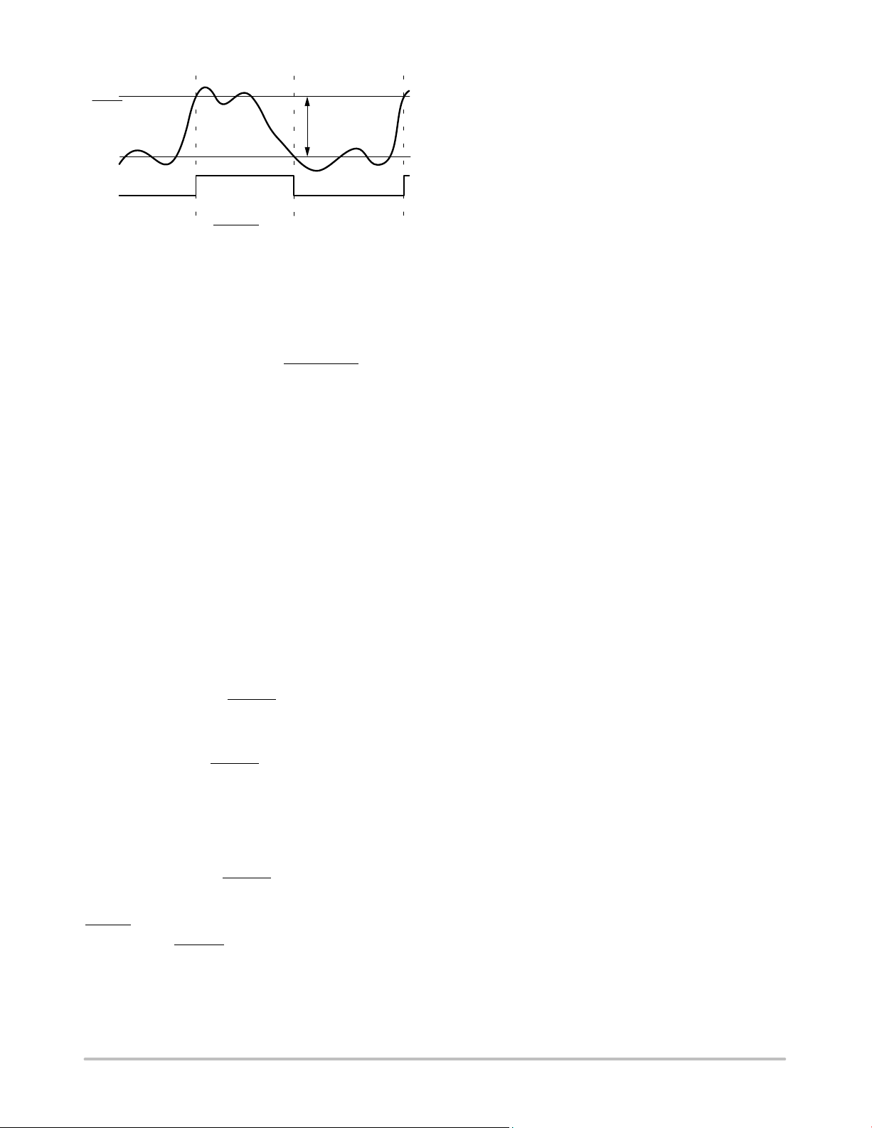
hysteresis; this can be disabled by setting the boost bit in
Configuration Register 3 (0x78), Bit 2. The hysteresis value
for that THERM
limit is the value programmed into the
hysteresis registers (Register 0x6D and Register 0x6E). The
default hysteresis value is 4°C.
http://onsemi.com
18
Page 19
ADT7473
THERM LIMIT
HYSTERESIS (5C)
TEMPERATURE
FANS
Figure 28. THERM Limit Operation
Limits, Status Registers, and Interrupts
Limit Values
Associated with each measurement channel on the
ADT7473/ADT7473−1 are high and low limits. These can
form the basis of system status monitoring; a status bit can
be set for any out−of−limit condition and is detected by
polling the device. Alternatively, SMBALERT
can be generated to flag a processor or microcontroller of
out−of−limit conditions.
8−Bit Limits
The following is a list of 8−bit limits on the ADT7473/
ADT7473−1.
Voltage Limit Registers
Register 0x46, V
Register 0x47, V
Register 0x48, V
Register 0x49, V
Temperature Limit Registers
CCP
CCP
CC
CC
Register 0x4E, Remote 1 Temperature Low Limit = 0x01
default
Register 0x4F, Remote 1 Temperature High Limit = 0xFF
default
Register 0x6A, Remote 1 THERM
Register 0x50, Local Temperature Low Limit = 0x01 default
Register 0x51, Local Temperature High Limit = 0xFF default
Register 0x6B, Local THERM
default
Register 0x52, Remote 2 Temperature Low Limit = 0x01
default
Register 0x53, Remote 2 Temperature High Limit = 0xFF
default
Register 0x6C, Remote 2 THERM
default
THERM Limit Register
Register 0x7A, THERM Timer Limit = 0x00 default
16−Bit Limits
The fan TACH measurements are 16−bit results. The fan
TACH limits are also 16 bits, consisting of a high byte and
low byte. Because fans running under speed or stalled are
100%
interrupts
Low Limit = 0x00 default
High Limit = 0xFF default
Low Limit = 0x00 default
High Limit = 0xFF default
Limit = 0xA4 default
Temperature Limit = 0xA4
Temperature Limit = 0xA4
normally the only conditions of interest, only high limits
exist for fan TACHs. Because the fan TACH period is
actually being measured, exceeding the limit indicates a
slow or stalled fan.
Fan Limit Registers
Register 0x54, TACH1 Minimum Low Byte = 0xFF default
Register 0x55, TACH1 Minimum High Byte = 0xFF default
Register 0x56, TACH2 Minimum Low Byte = 0xFF default
Register 0x57, TACH2 Minimum High Byte = 0xFF default
Register 0x58, TACH3 Minimum Low Byte = 0xFF default
Register 0x59, TACH3 Minimum High Byte = 0xFF default
Register 0x5A, TACH4 Minimum Low Byte = 0xFF default
Register 0x5B, TACH4 Minimum High Byte = 0xFF default
Out−of−Limit Comparisons
Once all limits have been programmed, the ADT7473/
ADT7473−1 can be enabled for monitoring. The ADT7473/
ADT7473−1 measures all voltage and temperature
measurements in round−robin format and sets the
appropriate status bit for out−of−limit conditions. TACH
measurements are not part of this round−robin cycle.
Comparisons are done differently depending on whether the
measured value is being compared to a high or low limit.
High limit > comparison performed
Low limit ≤ comparison performed
Voltage and temperature channels use a window
comparator for error detecting and, therefore, have high and
low limits. Fan speed measurements use only a low limit.
This fan limit is needed only in manual fan control mode.
Analog Monitoring Cycle Time
The analog monitoring cycle begins when a 1 is written to
the start bit (Bit 0) of Configuration Register 1 (0x40). By
default, the ADT7473/ADT7473−1 powers up with this bit
set. The ADC measures each analog input in turn and, as
each measurement is completed, the result is automatically
stored in the appropriate value register. This round−robin
monitoring cycle continues unless disabled by writing a 0 to
Bit 0 of Configuration Register 1.
As the ADC is normally left to free−run in this manner, the
time taken to monitor all the analog inputs is normally not
of interest, because the most recently measured value of any
input can be read out at any time.
For applications where the monitoring cycle time is
important, it can easily be calculated. The total number of
channels measured is
• One dedicated supply voltage input (V
• Supply voltage (V
CC
pin)
CCP
)
• Local temperature
• Two remote temperatures
As mentioned previously, the ADC performs round−robin
conversions. The total monitoring cycle time for averaged
voltage and temperature monitoring is 146 ms. The total
http://onsemi.com
19
Page 20
ADT7473
monitoring cycle time for voltage and temperature
monitoring with averaging disabled is 19 ms. The ADT7473/
ADT7473−1 is a derivative of the ADT7467. As a result, the
total conversion time in the ADT7473/ ADT7473−1 is the
same as the total conversion time of the ADT7467, even
though the ADT7473/ADT7473−1 has fewer monitored
channels.
Fan TACH measurements are made in parallel and are not
synchronized with the analog measurements in any way.
Interrupt Status Registers
The results of limit comparisons are stored in Interrupt
Status Register 1 and Interrupt Status Register 2. The status
register bit for each channel reflects the status of the last
measurement and limit comparison on that channel. If a
measurement is within limits, the corresponding status
register bit is cleared to 0. If the measurement is out of limits,
the corresponding status register bit is set to 1.
The state of the various measurement channels can be
polled by reading the status registers over the serial bus. In
Bit 7 (OOL) of Interrupt Status Register 1 (Reg. 0x41), a 1
means an out−of−limit event has been flagged in Interrupt
Status Register 2. This means the user needs only to read
Interrupt Status Register 2 when this bit is set. Alternatively,
Pin 5 or Pin 9 on the ADT7473 can be configured as an
SMBALERT
be an SMBALERT
output, while only Pin 9 can be configured to
on the ADT7473−1. This automatically
notifies the system supervisor of an out−of−limit condition.
Reading the status registers clears the appropriate status bit
as long as the error condition that caused the interrupt has
cleared. Status register bits (except OVT) are sticky.
Whenever a status bit is set, indicating an out−of−limit
condition, it remains set even if the event that caused it has
gone away (until read). The only way to clear the status bit
is to read the status register after the event has gone away.
Interrupt mask registers (Register 0x74 and Register 0x75)
allow individual interrupt sources to be masked from
causing an SMBALERT
. However, if one of these masked
interrupt sources goes out of limit, its associated status bit is
set in the interrupt status registers. OVT clears
automatically.
Interrupt Status Register 1 (0x41)
Bit 7 (OOL) = 1, denotes a bit in Interrupt Status Register 2
is set and Interrupt Status Register 2 should be read.
Bit 6 (R2T) = 1, Remote 2 temperature high or low limit has
been exceeded.
Bit 5 (LT) = 1, local temperature high or low limit has been
exceeded.
Bit 4 (R1T) = 1, Remote 1 temperature high or low limit has
been exceeded.
Bit 2 (V
Bit 1 (V
Interrupt Status Register 2 (0x42)
) = 1, VCC high or low limit has been exceeded.
CC
CCP
) = 1, V
high or low limit has been exceeded.
CCP
Bit 7 (D2) = 1, indicates an open or short on D2+/D2– inputs.
Bit 6 (D1) = 1, indicates an open or short on D1+/D1– inputs.
Bit 5 (F4P) = 1, indicates Fan 4 has dropped below the
minimum speed. Alternatively, it indicates the THERM
limit has been exceeded, if the THERM function is used.
Bit 4 (FAN3) = 1, indicates Fan 3 has dropped below the
minimum speed.
Bit 3 (FAN2) = 1, indicates Fan 2 has dropped below the
minimum speed.
Bit 2 (FAN1) = 1, indicates that Fan 1 dropped below the
minimum speed.
Bit 1 (OVT) = 1, indicates that a THERM
overtemperature
limit has been exceeded.
Bit 0 (THERM
Limit Latch) = 1, indicates a Remote
Channel 2 latch.
SMBALERT Interrupt Behavior
The ADT747/ADT7473−1 can be polled for status, or an
SMBALERT
interrupt can be generated for out−of−limit
conditions. It is important to note how the SMBALERT
output and status bits behave when writing interrupt handler
software.
HIGH LIMIT
TEMPERATURE
CLEARED ON READ
STICKY
STATUS BIT
TEMP BACK IN LIMIT
SMBALERT
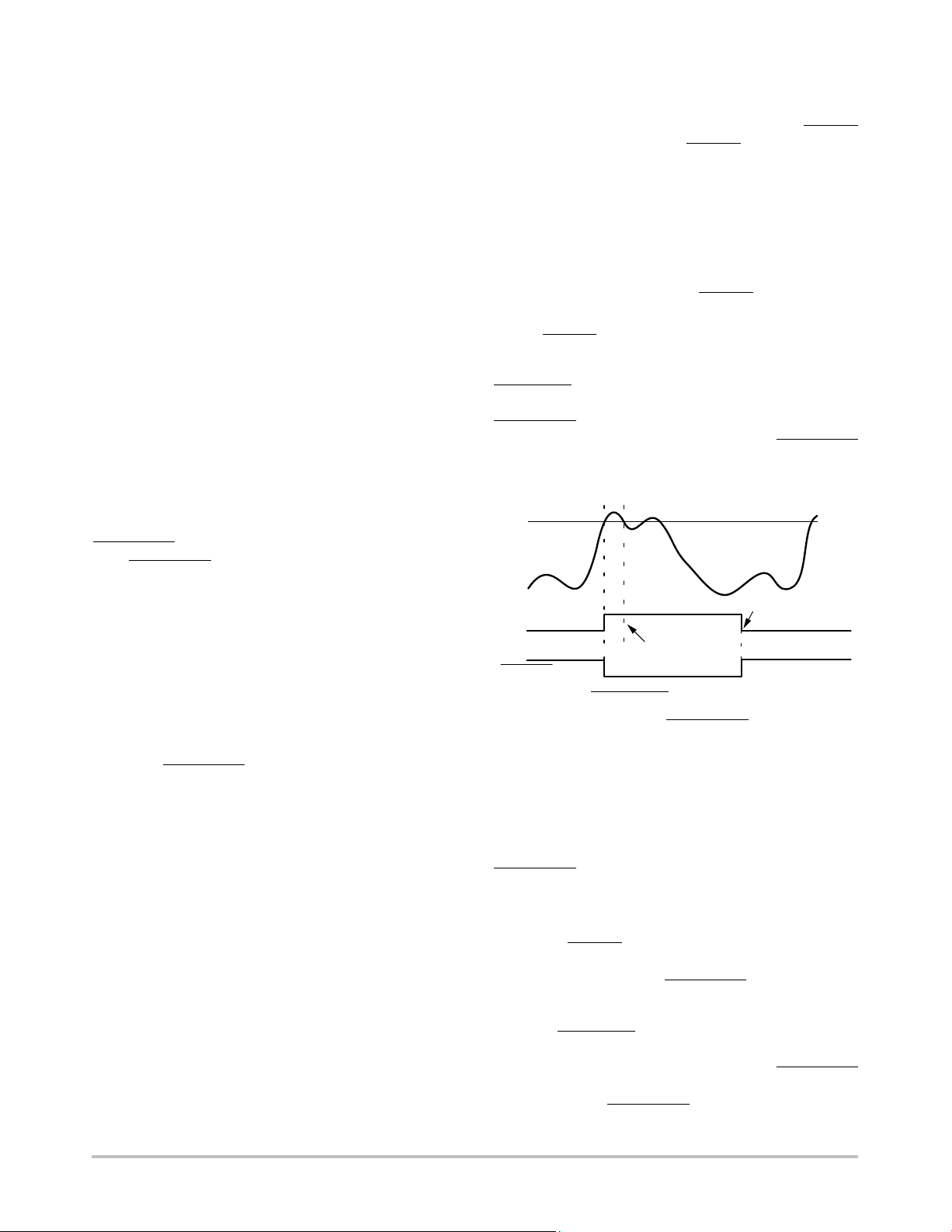
Figure 29. SMBALERT and Status Bit Behavior
(STATUS BIT STAYS SET)
(TEMP BELOW LIMIT)
Figure 29 shows how the SMBALERT output and sticky
status bits behave. Once a limit is exceeded, the
corresponding status bit is set to 1. The interrupt status bit
remains set until the error condition subsides and the
interrupt status register is read. The status bits are referred
to as sticky because they remain set until read by software.
This ensures that an out−of−limit event cannot be missed if
software is polling the device periodically. Note that the
SMBALERT
output remains low for the entire duration that
a reading is out of limit and until the interrupt status register
has been read. This has implications on how software
handles the interrupt.
Note that THERM
overtemperature events are not sticky,
resetting immediately after the overtemperature condition
ceases. This also applies to SMBALERT
if associated with
an OVT event.
Handling SMBALERT Interrupts
To prevent the system from being tied up servicing
interrupts, it is recommended to handle the SMBALERT
interrupt as follows:
1. Detect the SMBALERT
assertion.
2. Enter the interrupt handler.
http://onsemi.com
20
Page 21
ADT7473
3. Read the status registers to identify the interrupt
source.
4. Mask the interrupt source by setting the
appropriate mask bit in the interrupt mask registers
(Register 0x74 and Register 0x75).
5. Take the appropriate action for a given interrupt
source.
6. Exit the interrupt handler.
Periodically poll the status registers. If the interrupt status
bit has cleared, reset the corresponding interrupt mask bit
to 0. This causes the SMBALERT
output and status bits to
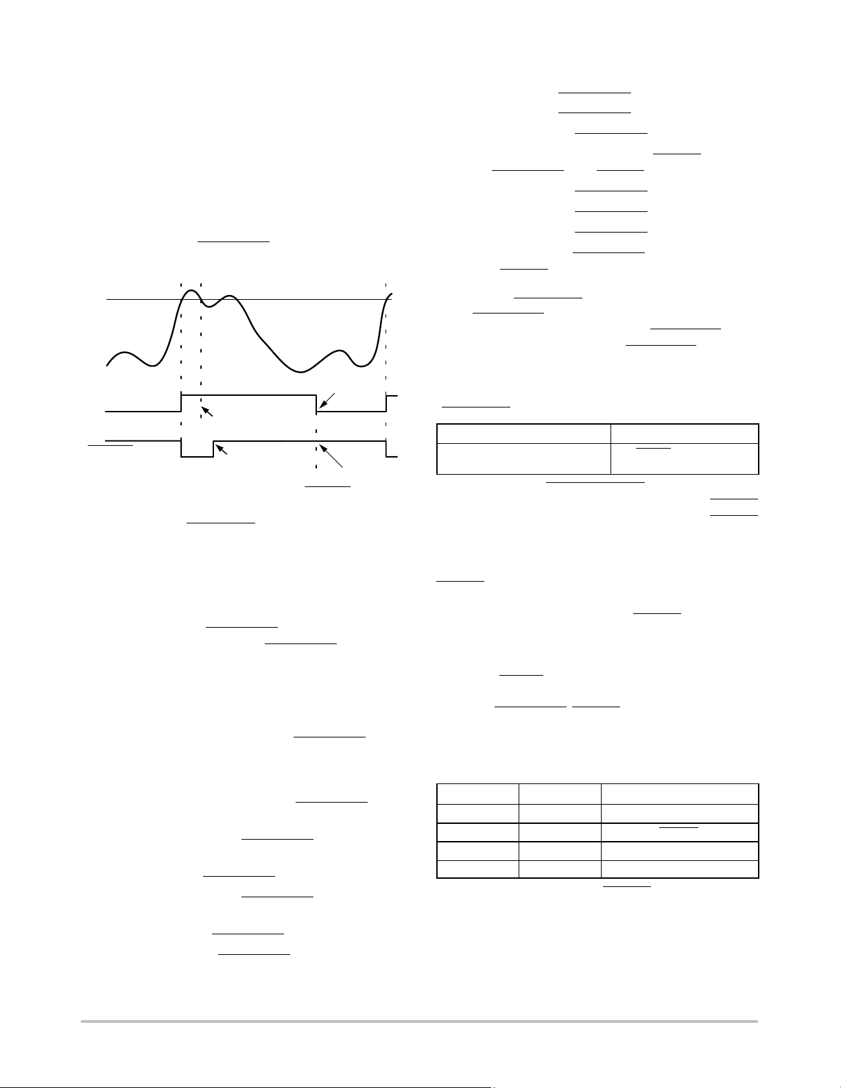
behave as shown in Figure 30.
HIGH LIMIT
TEMPERATURE
CLEARED ON READ
STICKY
STATUS BIT
TEMP BACK IN LIMIT
(STATUS BIT STAYS SET)
SMBALERT
Figure 30. How Masking the Interrupt Source Affects
SMBALERT
Masking Interrupt Sources
INTERRUPT
MASK BIT SET
Output
(TEMP BELOW LIMIT)
INTERRUPT MASK BIT
CLEARED
(SMBALERT RE−ARMED)
Register 0x74, Interrupt Mask Register 1
Register 0x75, Interrupt Mask Register 2
These registers allow individual interrupt sources to be
masked out to prevent SMBALERT
interrupt source prevents only the SMBALERT
interrupts. Masking an
output from
being asserted; the appropriate status bit is set normally.
Interrupt Mask Register 1 (0x74)
Bit 7 (OOL) = 0, when one or more alerts are generated in
Interrupt Status Register 2, assuming all the mask bits in the
Interrupt Mask Register 2 (0x75) =1; SMBALERT
is still
asserted.
OOL=1, when one or more alerts are generated in
Interrupt Status Register 2, assuming all the mask bits in the
Interrupt Mask Register 2 (0x75) =1; SMBALERT
is not
asserted.
Bit 6 (R2T) = 1, masks SMBALERT
for Remote 2
temperature
Bit 5 (LT) = 1, masks SMBALERT
Bit 4 (R1T) = 1, masks SMBALERT
for local temperature.
for Remote 1
temperature.
Bit 2 (V
Bit 1 (V
) = 1, masks SMBALERT for VCC channel.
CC
) = 1, masks SMBALERT for V
CCP
CCP
channel.
Interrupt Mask Register 2 (Reg. 0x75)
Bit 7 (D2) = 1, masks SMBALERT for Diode 2 errors.
Bit 6 (D1) = 1, masks SMBALERT
for Diode 1 errors.
Bit 5 (FAN4) = 1, masks SMBALERT for Fan 4 failure.
If the TACH4 pin is being used as the THERM
bit masks SMBALERT
Bit 4 (FAN3) = 1, masks SMBALERT
Bit 3 (FAN2) = 1, masks SMBALERT
Bit 2 (FAN1) = 1, masks SMBALERT
Bit 1 (OVT) = 1, masks SMBALERT
(exceeding THERM
Enabling the SMBALERT Interrupt Output
for a THERM event.
for Fan 3.
for Fan 2.
for Fan 1.
for overtemperature
limits).
input, this
The SMBALERT interrupt function is disabled by default.
Pin 5 or Pin 9 can be reconfigured as an SMBALERT
to signal out−of−limit conditions. (SMBALERT
output
function is
available only on Pin 9 of ADT7473−1.)
Table 11. ADT7473 Configuring Pin 5 as
SMBALERT
Configuration Register 3
(Register 0x78)
Output
Register Bit Setting
[0] ALERT = 1
The ADT7473−1 THERM_LATCH function latches and
asserts when temperature rises 0.25°C above the THERM
limit for the selected remote channel. Due to a THERM
event, the fans spin at full speed. This can be disabled by
setting Bit 2 in Configuration Register 0x7D.
Pin 5 remains latched until temperature falls below
THERM
limit for the selected zone, Remote Channel D1 or
Remote Channel D2, and Bit 0 in Status Register 2 is cleared.
By default on the ADT7473−1, the THERM
limit is set as
136°C for Remote Channel 2 and 100°C for Remote
Channel 1.
Assigning THERM Functionality to a Pin
Pin 9 on the ADT7473/ADT7473−1 has four possible
functions: SMBALERT
, THERM, GPIO, and TACH4. The
user chooses the required functionality by setting Bit 0 and
Bit 1 of Configuration Register 4 (0x7D).
Table 12.
Bit 1 Bit 0 Function
0 1 TACH4
0 0 THERM
1 1 SMBusALERT
1 0 GPIO
Once Pin 9 is configured as THERM, it must be enabled
by setting Bit 1 of Configuration Register 3 (0x78).
http://onsemi.com
21
Page 22
ADT7473
THERM as an Input
When THERM is configured as an input, the
ADT7473/ADT7473−1 can time assertions on the THERM
pin. This can be useful for connecting to the PROCHOT
output of a CPU to gauge system performance. See the
THERM
Timer section for more information.
The user can also set up the ADT7473/ADT7473−1 so
that, when the THERM
pin is driven low externally, the fans
run at 100%. The fans run at 100% for the duration of the
time the THERM
pin is pulled low. This is done by setting
the BOOST bit (Bit 2) in Configuration Register 3 (0x78)
to 1. This works only if the fan is already running, for
example, in manual mode when the current duty cycle is
above 0x00, or in automatic mode when the temperature is
above T
. If the temperature is below T
MIN
or if the duty
MIN
cycle in manual mode is set to 0x00, then pulling the
THERM
low externally has no effect. See Figure 31 for
more information.
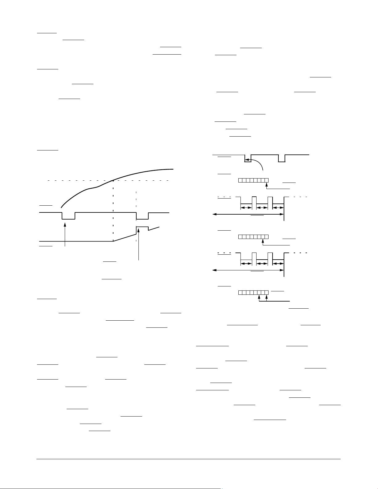
T
MIN
THERM
the LSB of the timer with a resolution of 22.76 ms (see
Figure 32).
When using the THERM
After a THERM
timer read (0x79):
timer, be aware of the following.
1. The contents of the timer are cleared on read.
2. The F4P bit (Bit 5) of Interrupt Status Register 2
needs to be cleared (assuming that the THERM
timer limit has been exceeded).
If the THERM
timer is read during a THERM assertion,
then the following happens:
1. The contents of the timer are cleared.
2. Bit 0 of the THERM
THERM
3. The THERM
assertion is occurring).
timer increments from 0.
4. If the THERM
timer is set to 1 (because a
timer limit (Register 0x7A) = 0x00,
the F4P bit is set.
THERM
000 0001
THERM
TIMER
(REG. 0x79)
THERM
ACCUMULATE THERM LOW
ASSERTION TIMES
7 6 532 104
0
THERM ASSERTED
≤ 22.76ms
THERM ASSERTED TO LOW AS AN INPUT:
FANS DO NOT GO TO 100% BECAUSE
TEMPERATURE IS BELOW T
.
MIN
THERM ASSERTED TO LOW AS AN INPUT:
FANS DO NOT GO TO 100% BECAUSE
TEMPERATURE IS ABOVE T
MIN
Figure 31. Asserting THERM Low as an Input in
Automatic Fan Speed Control Mode
THERM Timer
The ADT7473/ADT7473−1 has an internal timer to
measure THERM
assertion time. For example, the THERM
input can be connected to the PROCHOT output of a Pentium
4 CPU to measure system performance. The THERM
input
can also be connected to the output of a trip point temperature
sensor.
The timer is started on the assertion of the
ADT7473/ADT7473−1 THERM
THERM
is deasserted. The timer counts THERM times
input and stopped when
cumulatively; that is, the timer resumes counting on the next
THERM
accumulate THERM
assertion. The THERM timer continues to
assertion times until the timer is read (it
is cleared on read) or until it reaches full scale. If the counter
reaches full scale, it stops at that reading until cleared.
The 8−bit THERM
so that Bit 0 is set to 1 on the first THERM
the cumulative THERM
45.52 ms, Bit 1 of the THERM
timer status register (0x79) is designed
assertion. Once
assertion time has exceeded
timer is set and Bit 0 becomes
000 0010
THERM
TIMER
(REG. 0x79)
THERM
ACCUMULATE THERM LOW
ASSERTION TIMES
THERM
TIMER
(REG. 0x79)
0
7 6 532 104
000 0101
0
7 6 532 104
THERM ASSERTED
≥ 45.52ms
THERM ASSERTED ≥ 113.8ms
(91.04ms + 22.76ms)
Figure 32. Understanding the THERM Timer
Generating SMBALERT Interrupts from THERM Timer
Events
The ADT7473/ADT7473−1 can generate an
SMBALERT
when a programmable THERM timer limit is
exceeded. This allows the system designer to ignore brief,
infrequent THERM
THERM
timer events. Register 0x7A is the THERM timer
assertions, while capturing longer
limit register. This 8−bit register allows a limit from 0 sec
(first THERM
SMBALERT
compared with the contents of the THERM
register. If the THERM
assertion) to 5.825 sec to be set before an
is generated. The THERM timer value is
timer limit
timer value exceeds the THERM
timer limit value, the F4P bit (Bit 5) of Interrupt Status
Register 2 is set and an SMBALERT
is generated. The F4P
bit (Bit 5) of Interrupt Mask Register 2 (0x75) masks out the
http://onsemi.com
22
Page 23

ADT7473
SMBALERT if this bit is set to 1; however, the F4P bit of
Interrupt Status Register 2 still is set if the THERM
timer
limit is exceeded.
Figure 33 is a functional block diagram of the THERM
timer, limit, and associated circuitry. Writing a value of 0x00
to the THERM
SMBALERT
A THERM
SMBALERT
timer limit register (0x7A) causes an
to be generated on the first THERM assertion.
timer limit value of 0x01 generates an
once cumulative THERM assertions exceed
45.52 ms.
Configuring the THERM Behavior
1. Configure Pin 9 as a THERM timer input. Setting
Bit 1 (THERM
Register 3 (0x78) enables the THERM
timer enable) of Configuration
timer
monitoring functionality. This is disabled on Pin 9
by default. Setting Bit 0 and Bit 1 (PIN9FUNC) of
Configuration Register 4 (0x7D) enables THERM
timer/output functionality on Pin 9 (Bit 1 of
Configuration Register 3, THERM
, must also be
set). Pin 9 can also be used as TACH4. Setting
Bit 5, Bit 6, and Bit 7 of Configuration Register 5
(0x7C) makes THERM
bidirectional. This means
that if the appropriate temperature channel exceeds
the THERM
asserts. If the ADT7473 is not pulling THERM
but THERM
temperature limit, the THERM output
low,
is pulled low by an external device
(such as a CPU overtemperature signal), the
THERM
timer also times THERM assertions. If
Bit 5, Bit 6, and Bit 7 of Configuration Register 5
(0x7C) are set to 0, THERM
is set as a timer input
only.
2. Select the desired fan behavior for THERM
timer
events. Assuming the fans are running, setting
Bit 2 (BOOST) of Configuration Register 3 (0x78)
causes all fans to run at 100% duty cycle whenever
THERM
is asserted. This allows fail−safe system
cooling. If this bit is 0, the fans run at their current
settings and are not affected by THERM events. If
the fans are not already running when THERM
is
asserted, the fans do not run at full speed.
3. Select whether THERM
generate SMBALERT
timer events should
interrupts. Bit 5 (F4P) of
Interrupt Mask Register 2 (0x75), when set, masks
out the SMBALERT
when the THERM timer limit
value is exceeded. This bit should be cleared if
SMBALERT
4. Select a suitable THERM
determines whether an SMBALERT
the first THERM
THERM
0x00 causes an SMBALERT
first THERM
5. Select a THERM
is based on THERM events required.
limit value. This value
is generated on
assertion, or only if a cumulative
assertion time limit is exceeded. A value of
to be generated on the
assertion.
monitoring time. This value
specifies how often OS or BIOS level software
checks the THERM
could read the THERM
determine the cumulative THERM
If, for example, the total THERM
timer. For example, BIOS
timer once an hour to
assertion time.
assertion time is
<22.76 ms in Hour 1, >182.08 ms in Hour 2, and
>5.825 sec in Hour 3, this can indicate that system
performance is degrading significantly because
THERM
is asserting more frequently on an hourly
basis.
Alternatively, OS− or BIOS−level software can timestamp
when the system is powered on. If an SMBALERT
generated due to the THERM
timer limit being exceeded,
is
another timestamp can be taken. The difference in time can
be calculated for a fixed THERM
example, if it takes one week for a THERM
timer limit time. For
timer limit of
2.914 seconds to be exceeded and the next time it takes only
one hour, this is an indication of a serious degradation in
system performance.
http://onsemi.com
23
Page 24
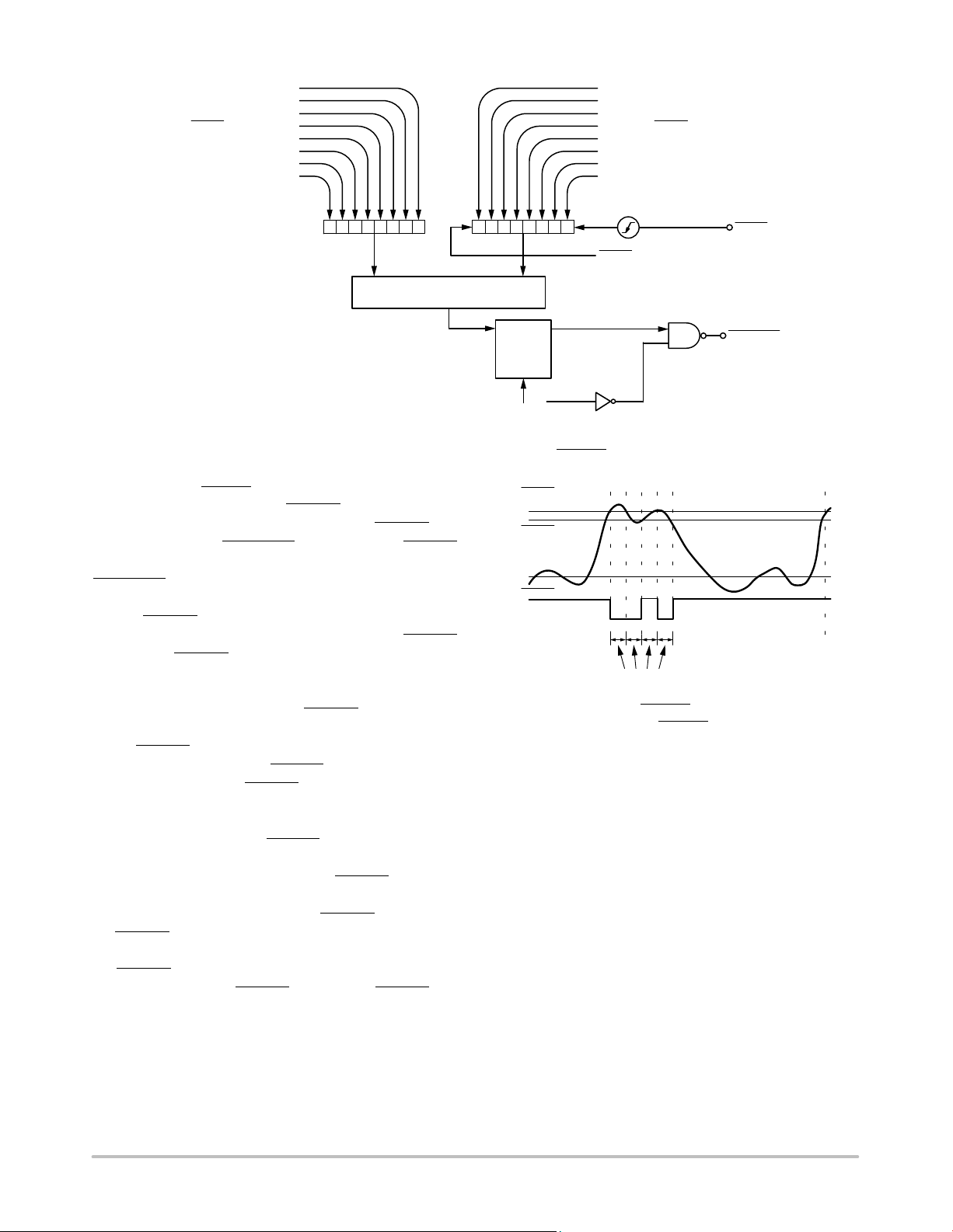
ADT7473
2.914s
1.457s
728.32ms
THERM
TIMER LIMIT
(REGISTER 0x7A)
364.16ms
182.08ms
91.04ms
45.52ms
22.76ms
2
1
0
6
7
543
COMPARATOR
Figure 33. Functional Block Diagram of the ADT7473 THERM Monitoring Circuitry
Configuring the THERM Pin as Bidirectional
In addition to monitoring THERM as an input, the
ADT7473/ADT7473−1 can optionally drive THERM
as an output. When PROCHOT
is bidirectional, THERM
low
can be used to throttle the processor by asserting
PROCHOT
. The user can preprogram system−critical
thermal limits. If the temperature exceeds a thermal limit by
0.25°C, THERM
asserts low. If the temperature is still above
the thermal limit on the next monitoring cycle, THERM
stays low. THERM remains asserted low until the
temperature is equal to or below the thermal limit. Because
the temperature for that channel is measured only once for
every monitoring cycle after THERM
asserts, it is
guaranteed to remain low for at least one monitoring cycle.
The THERM
Remote 1, local, or Remote 2 THERM
exceeded by 0.25°C. The THERM
pin can be configured to assert low, if the
temperature limits are
temperature limit registers
are at Register 0x6A, Register 0x6B, and Register 0x6C,
respectively. Setting Bit 5, Bit 6, and Bit 7 of Configuration
Register 5 (0x7C) makes THERM
bidirectional for the
Remote 1, local, and Remote 2 temperature channels,
respectively. Figure 34 shows how the THERM
pin asserts
low as an output in the event of a critical overtemperature.
An alternative method of disabling THERM
the THERM
temperature limit to –64°C or less in Offset 64
is to program
mode, or −128°C or less in twos complement mode; that is,
for THERM
–128°C, respectively, THERM
temperature limit values less than –63°C or
is disabled. THERM can
also be disabled by setting Bit 1 of Configuration Register 3
(0x78) to 0.
2.914s
1.457s
6
7
54321
IN
CLEARED
ON READ
OUT
LATCH
RESET
THERM LIMIT
0.255C
THERM LIMIT
TEMP
THERM
1 = MASK
728.32ms
364.16ms
182.08ms
91.04ms
45.52ms
22.76ms
0
THERM TIMER CLEARED ON READ
F4P BIT (BIT 5)
INTERRUPT STATUS
REGISTER 2
INTERRUPT MASK REGISTER 2
THERM TIMER
(REGISTER 0x79)
F4P BIT (BIT 5)
(REGISTER 0x75)
MONITORING
CYCLE
THERM
SMBALERT
Figure 34. Asserting THERM as an Output, Based on
Tripping THERM
Limits
Fan Drive Using PWM Control
The ADT7473/ADT7473−1 uses pulse−width modulation
(PWM) to control fan speed. This relies on varying the duty
cycle (or on/off ratio) of a square wave applied to the fan to
vary the fan speed. The external circuitry required to drive a
fan using PWM control is extremely simple. For 4−wire fans,
the PWM drive might need only a pullup resistor. In many
cases, the 4−wire fan PWM input has a built−in pullup
resistor.
The ADT7473/ADT7473−1 PWM frequency can be set to
a selection of low frequencies or a single high PWM
frequency. The low frequency options are usually used for
3−wire fans, while the high frequency option is usually used
with 4−wire fans.
Note that care must be taken to ensure that the PWM or
TACH pins are not connected to a pullup supply greater than
3.6 V.
http://onsemi.com
24
Page 25
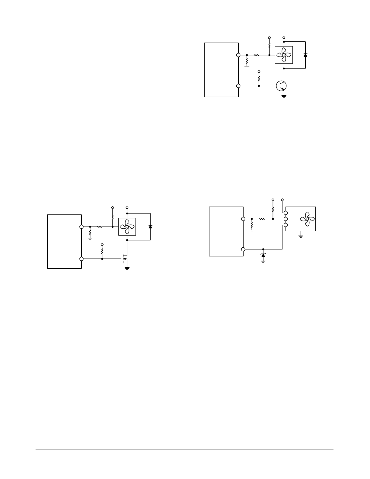
ADT7473
Many fans have internal pullups connected to the
TACH/PWM pins to a supply greater than 3.6 V. Clamping
or dividing down the voltage on these pins must be done
where necessary. Clamping these pins with a Zener diode
can also help prevent back−EMF related noise from being
coupled into the system.
For 3−wire fans, a single N−channel MOSFET is the only
drive device required. The specifications of the MOSFET
depend on the maximum current required by the fan being
driven. Typical notebook fans draw a nominal 170 mA;
therefore, SOT devices can be used where board space is a
concern. In desktops, fans can typically draw 250 mA to
300 mA each. If you drive several fans in parallel from a
single PWM output or drive larger server fans, the MOSFET
must handle the higher current requirements. The only other
stipulation is that the MOSFET have a gate voltage drive,
V
< 3.3 V, for direct interfacing to the PWM output. The
GS
MOSFET should also have a low on resistance to ensure that
there is not significant voltage drop across the FET, which
would reduce the voltage applied across the fan and,
therefore, the maximum operating speed of the fan.
Figure 35 shows how to drive a 3−wire fan using PWM
control.
12V 12V
10kΩ
TACH
ADT7473/
ADT7473−1
PWM
10kΩ
4.7kΩ
3.3V
10kΩ
12V
FAN
Q1
NDT3055L
1N4148
12V 12V
10kΩ
TACH
ADT7473/
ADT7473−1
PWM
10kΩ
4.7kΩ
665Ω
TACH
3.3V
12V
FAN
Q1
MMBT2222
1N4148
Figure 36. Driving a 3−Wire Fan Using an NPN
Transistor
Because 4−wire fans are powered continuously, the fan
speed is not switched on or off as with previous PWM
driven/powered fans. This enables it to perform better than
3−wire fans, especially for high frequency applications.
Figure 37 shows a typical drive circuit for 4−wire fans. As
the PWM input on 4−wire fans is usually internally pulled
up to a voltage greater than 3.6 V (the maximum voltage
allowed on the ADT7473/ADT7473−1 PWM output), the
PWM output should be clamped to 3.3 V using a Zener
diode.
12V 12V
12V, 4−WIRE FAN
V
CC
TACH
PWM
TACH
ADT7473/
ADT7473−1
PWM
10kΩ
4.7kΩ
10kΩ
TACH
3.3V
Figure 35. Driving a 3−Wire Fan Using an N−Channel
MOSFET
Figure 35 uses a 10 kW pullup resistor for the TACH
signal. This assumes that the TACH signal is an
open−collector from the fan. In all cases, the TACH signal
from the fan must be kept below 3.6 V maximum to prevent
damaging the ADT7473/ADT7473−1. If uncertain as to
whether the fan used has an open−collector or totem pole
TACH output, use one of the input signal conditioning
circuits shown in the Fan Speed Measurement section.
Figure 36 shows a fan drive circuit using an NPN
transistor such as a general−purpose MMBT2222. While
these devices are inexpensive, they tend to have much lower
current handling capabilities and higher on resistance than
MOSFETs. When choosing a transistor, care should be taken
to ensure that it meets the fan’s current requirements.
Ensure that the base resistor is chosen so that the transistor
is saturated when the fan is powered on.
Figure 37. Driving a 4−Wire Fan
Driving Two Fans from PWM3
The ADT7473/ADT7473−1 has four TACH inputs
available for fan speed measurement, but only three PWM
drive outputs. If a fourth fan is used in the system, it should
be driven from the PWM3 output in parallel with the third
fan. Figure 38 shows how to drive two fans in parallel using
low cost NPN transistors. Figure 39 shows the equivalent
circuit using a MOSFET.
Because the MOSFET can handle up to 3.5 A, it is simply
a matter of connecting another fan directly in parallel with
the first. Care should be taken in designing drive circuits
with transistors and FETs to ensure the PWM pins are not
required to source current and that they sink less than the
8 mA maximum current specified on the data sheet.
http://onsemi.com
25
Page 26
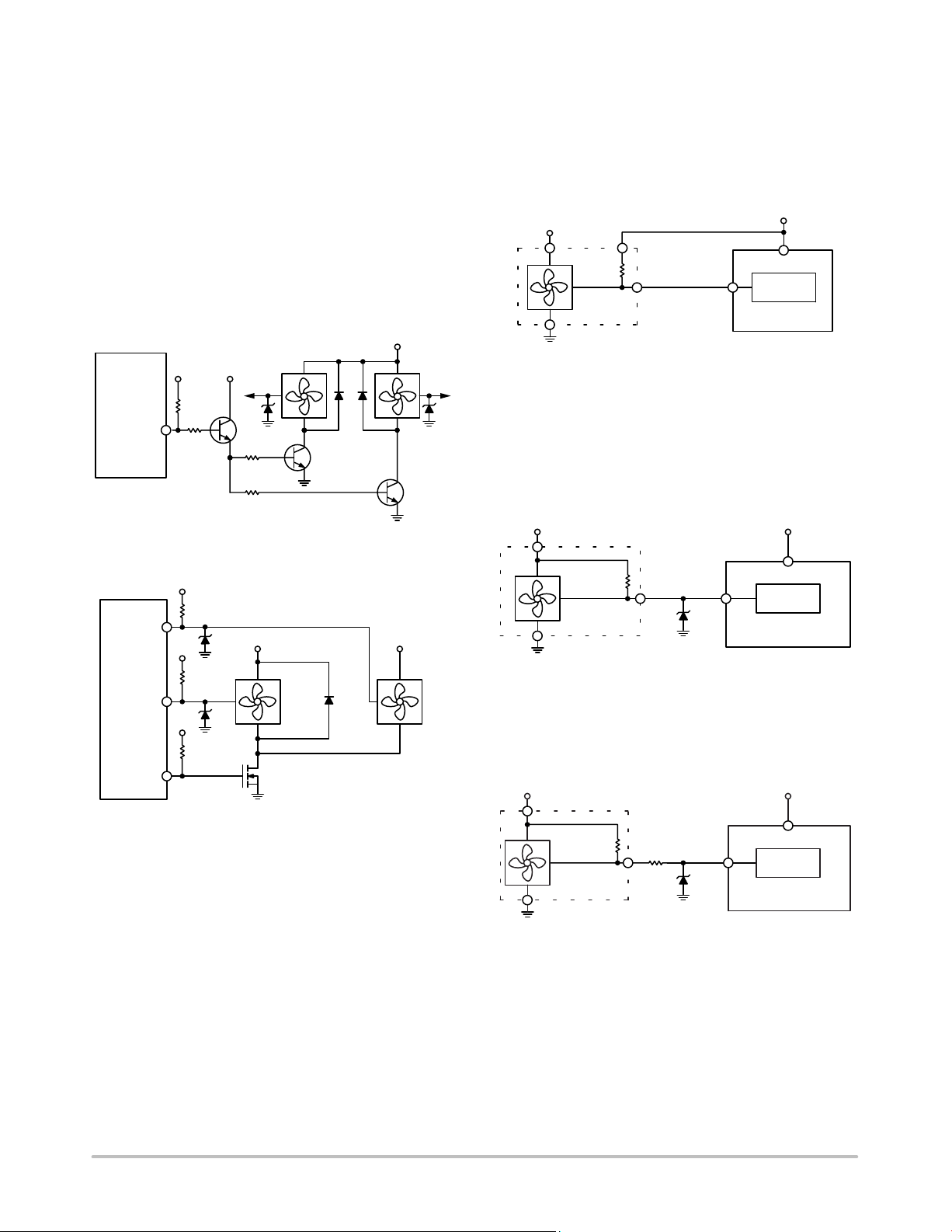
ADT7473
Driving up to Three Fans from PWM3
TACH measurements for fans are synchronized to
particular PWM channels; for example, TACH1 is
synchronized to PWM1. TACH3 and TACH4 are both
synchronized to PWM3, so PWM3 can drive two fans.
Alternatively, PWM3 can be programmed to synchronize
TACH2, TACH3, and TACH4 to the PWM3 output. This
allows PWM3 to drive two or three fans. In this case, the
drive circuitry looks the same, as shown in Figure 38 and
Figure 39. The SYNC bit in Register 0x62 enables this
function.
Synchronization is not required in high frequency mode
when used with 4−wire fans.
12V
ADT7473/
ADT7473−1
PWM3
Figure 38. Interfacing Two Fans in Parallel to the
PWM3 Output UsingLow Cost NPN Transistors
TACH4
ADT7473/
ADT7473−1
TACH3
PWM3
3.3V 3.3V
1k
W
2.2k
W
3.3V
10kΩ
TYPICAL
3.3V
3.3V
10kΩ
TYPICAL
TACH
3.3V
3.3V
10kΩ
TYPICAL
TACH3
Q2
MMBT2222
MMBT2222
1N4148
TACH
1N4148
Q3
3.3V
Q1
MMBT3904
W
10k
10k
W
+V +V
5V OR
12V FAN
Q1
NDT3055L
TACH4
5V OR
12V FAN
3.3V
of the fan signal or diode clamping must be included to keep
inputs within an acceptable range.
Figure 40 to Figure 43 show circuits for most common fan
TACH outputs.
If the fan TACH output has a resistive pullup to V
CC
, it can
be connected directly to the fan input, as shown in Figure 40.
V
12V
PULLUP
4.7kΩ
TYPICAL
TACH
OUTPUT
TACH
CC
FAN SPEED
COUNTER
ADT7473/
ADT7473-1
Figure 40. Fan with TACH Pullup to V
CC
If the fan output has a resistive pullup to 12 V (or other
voltage greater than 3.6 V), the fan output can be clamped
with a Zener diode, as shown in Figure 41. The Zener diode
voltage should be chosen so that it is greater than V
of the
IH
TACH input, but less than 3.6 V, allowing for the voltage
tolerance of the Zener. A value of between 3.0 V and 3.6 V
is suitable.
12V
PULLUP
4.7kΩ
TYPICAL
*CHOOSE ZD1 VOLTAGE APPROXIMATELY 0.8 y V
TACH
OUTPUT
TACH
ZD1*
Figure 41. Fan with TACH Pullup to Voltage > 3.6 V
Clamped with Zener Diode
V
CC
FAN SPEED
COUNTER
ADT7473/
ADT7473-1
CC
If the fan has a strong pullup (less than 1 kW) to 12 V or
a totem−pole output, a series resistor can be added to limit
the Zener current, as shown in Figure 42.
12V
V
CC
Figure 39. Interfacing Two Fans in Parallel to the
PWM3 Output Using a Single N−Channel MOSFET
Bit [4] (SYNC) of Enhanced Acoustics Register 1
(0x62)
SYNC = 1, synchronizes TACH2, TACH3, and TACH4 to
PWM3.
TACH Inputs
Pin 4, Pin 6, Pin 7, and Pin 9 (when configured as TACH
inputs) are open−drain TACH inputs intended for fan speed
measurement.
Signal conditioning in the ADT7473/ADT7473−1
accommodates the slow rise and fall times typical of fan
tachometer outputs. The maximum input signal range is 0 V
to 3.6 V. In the event that these inputs are supplied from fan
outputs that exceed 0 V to 3.6 V, either resistive attenuation
http://onsemi.com
PULLUP
4.7kΩ OR
TYPICAL
TACH
OUTPUT
TACH
ZD1
ZENER*
FAN SPEED
COUNTER
ADT7473/
ADT7473-1
*CHOOSE ZD1 VOLTAGE APPROXIMATELY 0.8 y V
Figure 42. Fan with Strong TACH Pullup to > VCC or
Totem−Pole Output, Clamped with Zener and Resistor
Alternatively, a resistive attenuator can be used, as shown
in Figure 43. R1 and R2 should be chosen such that
2Vt V
pullup
R2ńǒR
) R1 ) R2Ǔt 3.6 V
pullup
The fan inputs have an input resistance of nominally
160 kW to ground, which should be taken into account when
calculating resistor values.
26
CC
(eq. 3)
Page 27
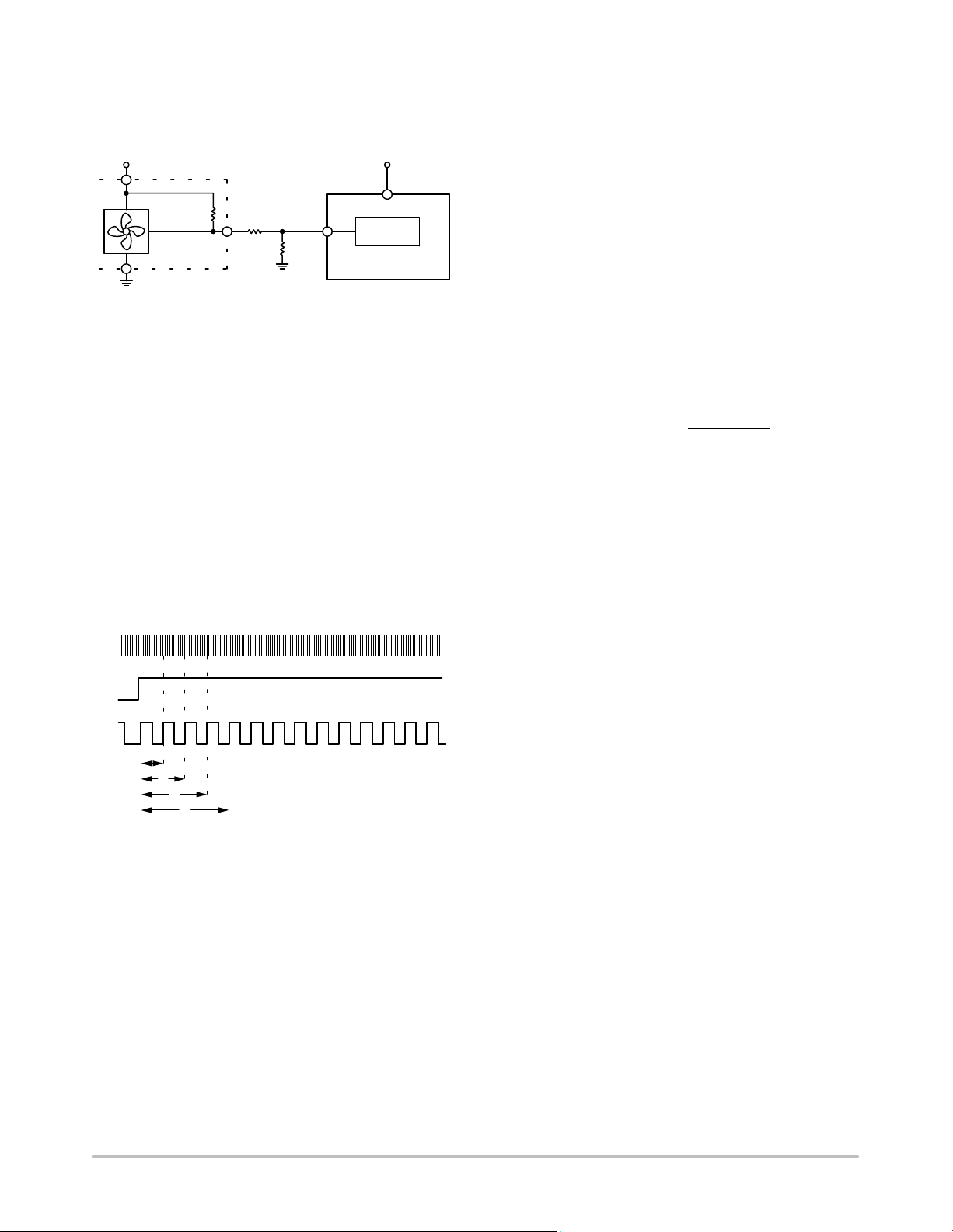
ADT7473
With a pullup voltage of 12 V and pullup resistor less than
1 kW, suitable values for R1 and R2 are 120 kW and 47 kW,
respectively. This gives a high input voltage of 3.35 V.
12V
<1kΩ
Figure 43. Fan with Strong TACH pullup to > V
Totem−Pole Output, Attenuated with R1/R2
Fan Speed Measurement
R1*
TACH
OUTPUT
TACH
R2*
*SEE TEXT
V
CC
FAN SPEED
COUNTER
ADT7473/
ADT7473-1
CC
or
The fan counter does not count the fan TACH output
pulses directly, because the fan speed could be less than
1000 RPM and it would take several seconds to accumulate
a reasonably large and accurate count. Instead, the period of
the fan revolution is measured by gating an on−chip 90 kHz
oscillator into the input of a 16−bit counter for N periods of
the fan TACH output (see Figure 44), so the accumulated
count is actually proportional to the fan tachometer period,
and inversely proportional to the fan speed.
N, the number of pulses counted, is determined by the
settings of the TACH pulses per revolution register (Register
0x7B). This register contains two bits for each fan, allowing
one, two (default), three, or four TACH pulses to be counted.
CLOCK
PWM
TACH
Fan Speed Measurement Registers
1
2
3
4
Figure 44. Fan Speed Measurement
The fan tachometer readings are 16−bit values consisting
of a 2−byte read from the ADT7473/ADT7473−1.
Register 0x28, TACH1 Low Byte = 0x00 default
Register 0x29, TACH1 High Byte = 0x00 default
Register 0x2A, TACH2 Low Byte = 0x00 default
Register 0x2B, TACH2 High Byte = 0x00 default
Register 0x2C, TACH3 Low Byte = 0x00 default
Register 0x2D, TACH3 High Byte = 0x00 default
Register 0x2E, TACH4 Low Byte = 0x00 default
Register 0x2F, TACH4 High Byte = 0x00 default
Reading Fan Speed from the ADT7473/ADT7473−1
The measurement of fan speeds involves a 2−register read
for each measurement. The low byte should be read first.
This causes the high byte to be frozen until both high and low
byte registers have been read, preventing erroneous TACH
readings. The fan tachometer reading registers report back
the number of 11.11 ms period clocks (90 kHz oscillator)
gated to the fan speed counter, from the rising edge of the
first fan TACH pulse to the rising edge of the third fan TACH
pulse (assuming two pulses per revolution are being
counted). Because the device is essentially measuring the
fan TACH period, the higher the count value, the slower the
fan is actually running. A 16−bit fan tachometer reading of
0xFFFF indicates either the fan has stalled or is running very
slowly (<100 RPM).
High Limit > Comparison Performed
Because the actual fan TACH period is measured, falling
below a fan TACH limit by 1 sets the appropriate status bit
and can be used to generate an SMBALERT
Measuring Fan TACH
.
When the ADT7473/ADT7473−1 starts up, TACH
measurements are locked. In effect, an internal read of the
low byte has been made for each TACH input. The net result
of this is that all TACH readings are locked until the high
byte is read from the corresponding TACH registers. All
TACH related interrupts are also ignored until the
appropriate high byte is read.
Once the corresponding high byte has been read, TACH
measurements are unlocked and interrupts are processed as
normal.
Fan TACH Limit Registers
The fan TACH limit registers are 16−bit values consisting
of two bytes.
Register 0x54, TACH1 Minimum Low Byte = 0xFF default
Register 0x55, TACH1 Minimum High Byte = 0xFF default
Register 0x56, TACH2 Minimum Low Byte = 0xFF default
Register 0x57, TACH2 Minimum High Byte = 0xFF default
Register 0x58, TACH3 Minimum Low Byte = 0xFF default
Register 0x59, TACH3 Minimum High Byte = 0xFF default
Register 0x5A, TACH4 Minimum Low Byte = 0xFF default
Register 0x5B, TACH4 Minimum High Byte = 0xFF default
Fan Speed Measurement Rate
The fan TACH readings are normally updated once every
second.
The FAST bit (Bit 3) of Configuration Register 3 (0x78),
when set, updates the fan TACH readings every 250 ms.
If any of the fans are not being driven by a PWM channel
but are powered directly from 5.0 V or 12 V, their associated
dc bit in Configuration Register 3 should be set. This allows
TACH readings to be taken on a continuous basis for fans
http://onsemi.com
27
Page 28

ADT7473
connected directly to a dc source. For optimal results, the
associated dc bit should always be set when using 4−wire
fans.
Calculating Fan Speed
Assuming a fan has two pulses per revolution (and two
pulses per revolution being measured), fan speed is
calculated by:
Fan Speed (RPM) = (90,000 x 60)/Fan TACH Reading
where Fan TACH Reading is the 16−bit fan tachometer
reading.
Example
TACH1 High Byte (Register 0x29) = 0x17
TACH1 Low Byte (Register 0x28) = 0xFF
What is Fan 1 speed in RPM?
Fan 1 TACH Reading = 0x17FF = 6143 (decimal)
RPM = (f x 60)/Fan 1 TACH Reading
RPM = (90000 x 60)/6143
Fan Speed = 879 RPM
Fan Pulses per Revolution
Different fan models can output either one, two, three, or
four TACH pulses per revolution. Once the number of fan
TACH pulses has been determined, it can be programmed
into the fan pulses per revolution register (Register 0x7B)
for each fan. Alternatively, this register can be used to
determine the number or pulses per revolution output by a
given fan. By plotting fan speed measurements at a 100%
speed with different pulses per revolution setting, the
smoothest graph with the lowest ripple determines the
correct pulses per revolution value.
TACH Pulses per Revolution Register
Bits [1:0] Fan 1 default = 2 pulses per revolution
Bits [3:2] Fan 2 default = 2 pulses per revolution
Bits [5:4] Fan 3 default = 2 pulses per revolution
Bits [7:6] Fan 4 default = 2 pulses per revolution
00 = 1 pulse per revolution
01 = 2 pulses per revolution
10 = 3 pulses per revolution
11 = 4 pulses per revolution
Fan Spin−Up
The ADT7473/ADT7473−1 has a unique fan spin−up
function. It spins the fan at 100% PWM duty cycle until two
TACH pulses are detected on the TACH input. Once two
TACH pulses are detected, the PWM duty cycle goes to the
expected running value, for example, 33%. The advantage
is that fans have different spin−up characteristics and take
different times to overcome inertia. The ADT7473/
ADT7473−1 runs the fans just fast enough to overcome
inertia and is quieter on spin−up than fans programmed for
a given spin−up time.
Fan Startup Timeout
To prevent the generation of false interrupts as a fan spins
up (because it is below running speed), the ADT7473/
ADT7473−1 includes a fan startup timeout function. During
this time, the ADT7473/ADT7473−1 looks for two TACH
pulses. If two TACH pulses are not detected, an interrupt is
generated. Using Configuration Register 1 (0x40), Bit 5
(FSPDIS), this functionality can be changed (see the
Disabling Fan Startup Timeout section).
PWM1, PWM2, PWM3 Configuration Registers
(Register 0x5C, Register 0x5D, and Register 0x5E)
Bits [2:0] SPIN, startup timeout for PWM1 = 0x5C,
PWM2 = 0x5D, and PWM3 = 0x5E.
000 = No startup timeout
001 = 100 ms
010 = 250 ms default
011 = 400 ms
100 = 667 ms
101 = 1 sec
110 = 2 sec
111 = 4 sec
Disabling Fan Startup Timeout
Although fan startup makes fan spin−ups much quieter
than fixed−time spin−ups, the option exists to use fixed
spin−up times. Setting Bit 5 (FSPDIS) to 1 in Configuration
Register 1 (0x40) disables the spin−up for two TACH pulses.
Instead, the fan spins up for the fixed time as selected in
Register 0x5C to Register 0x5E.
PWM Logic State
The PWM outputs can be programmed high for a 100%
duty cycle (non−inverted) or low for a 100% duty cycle
(inverted).
PWM1 Configuration Register (0x5C)
Bit 4 INV.
0 = Logic high for a 100% PWM duty cycle
1 = Logic low for a 100% PWM duty cycle
PWM2 Configuration Register (0x5D)
Bit 4 INV.
0 = Logic high for a 100% PWM duty cycle
1 = Logic low for a 100% PWM duty cycle
PWM3 Configuration Register (0x5E)
Bit 4 INV.
0 = Logic high for a 100% PWM duty cycle
1 = Logic low for a 100% PWM duty cycle
Low Frequency Mode PWM Drive Frequency
The PWM drive frequency can be adjusted for the
application. Register 0x5F to Register 0x61 configure the
PWM frequency for PWM1 to PWM3, respectively. In high
frequency mode, the PWM drive frequency is always
22.5 kHz.
http://onsemi.com
28
Page 29

ADT7473
High Frequency Mode PWM Drive
Setting Bit 3 of Register 0x5F, 60H or 61H enables high
frequency mode for fans 1, 2 and 3.
PWM Frequency Registers
(Register 0x5F to Register 0x61)
Bits [2:0] FREQ
000 = 11.0 Hz
001 = 14.7 Hz
010 = 22.1 Hz
011 = 29.4 Hz
100 = 35.3 Hz (default)
101 = 44.1 Hz
110 = 58.8 Hz
111 = 88.2 Hz
Fan Speed Control
The ADT7473/ADT7473−1 controls fan speed using
automatic and manual modes.
In automatic fan speed control mode, fan speed is
automatically varied with temperature and without CPU
intervention, once initial parameters are set up. The
advantage of this is that, if the system hangs, the user is
guaranteed the system is protected from overheating. The
automatic fan speed control incorporates a feature called
dynamic T
calibration. This feature reduces the design
MIN
effort required to program the automatic fan speed control
loop. For more information and procedures on how to
program the automatic fan speed control loop and dynamic
T
calibration, see the Programming the Automatic Fan
MIN
Speed Control Loop section.
In manual fan speed control mode, the ADT7473/
ADT7473−1 allows the duty cycle of any PWM output to be
manually adjusted. This can be useful if the user wants to
change fan speed in software or adjust the PWM duty cycle
output for test purposes. Bits [7:5] of Register 0x5C to
Register 0x5E (PWM configuration registers) control the
behavior of each PWM output.
PWM Configuration Registers
(Register 0x5C to Register 0x5E)
Bits [7:5] BHVR
111 = manual mode
Once under manual control, each PWM output can be
manually updated by writing to Register 0x30 to Register
0x32 (PWM current duty cycle registers).
Programming the PWM Current Duty Cycle Registers
The PWM current duty cycle registers are 8−bit registers
that allow the PWM duty cycle for each output to be set
anywhere from 0% to 100% in steps of 0.39%.
The value to be programmed into the PWM
register is
MIN
given by:
Value (decimal) = PWM
MIN
/0.39
Example 1
For a PWM duty cycle of 50%
Value (decimal) = 50/0.39 = 128 (decimal)
Value = 128 (decimal) or 0x80 (hex)
Example 2
For a PWM duty cycle of 33%
Value (decimal) = 33/0.39 = 85 (decimal)
Value = 85 (decimal) or 0x54 (hex)
PWM Current Duty Cycle Registers
Register 0x30, PWM1 Duty Cycle = 0x00 (0% default)
Register 0x31, PWM2 Duty Cycle = 0x00 (0% default)
Register 0x32, PWM3 Duty Cycle = 0x00 (0% default)
By reading the PWMx current duty cycle registers, the
user can keep track of the current duty cycle on each PWM
output, even when the fans are running in automatic fan
speed control mode or acoustic enhancement mode. See the
Programming the Automatic Fan Speed Control Loop
section for details.
Fan Presence Detect
This feature can be used to determine if a 4−wire fan is
directly connected to a PWM output. This feature does not
work for 3−wire fans. To detect whether a 4−wire fan is
connected directly to a PWM output, the following steps
must be performed in this order:
1. Drive the appropriate PWM outputs to 100% duty
cycle.
2. Set Bit 0 of Configuration Register 2 (0x73).
3. Wait 5 ms.
4. Program the fans to run at a different speed if
necessary.
5. Read the state of Bits [3:1] of Configuration
Register 2 (0x73). The state of these bits reflects
whether a 4−wire fan is directly connected to the
PWM output.
As the detection time only takes 5 ms, programming the
PWM outputs to 100% and then back to their normal speed
is not noticeable in most cases.
Description of How Fan Presence Detect Works
Typical 4−wire fans have an internal pull up to 4.75 V
±10%, which typically sources 5 mA. While the detection
cycle is on, an internal current sink is turned on, sinking
current from the fan’s internal pullup. By driving some of the
current from the fan’s internal pullup (~100 mA), the logic
buffer switches to a defined logic state. If this state is high,
a fan is present; if it is low, no fan is present.
The PWM input voltage should be clamped to 3.3 V. This
ensures the PWM output is not pulled to a voltage higher
than the maximum allowable voltage on that pin (3.6 V).
http://onsemi.com
29
Page 30
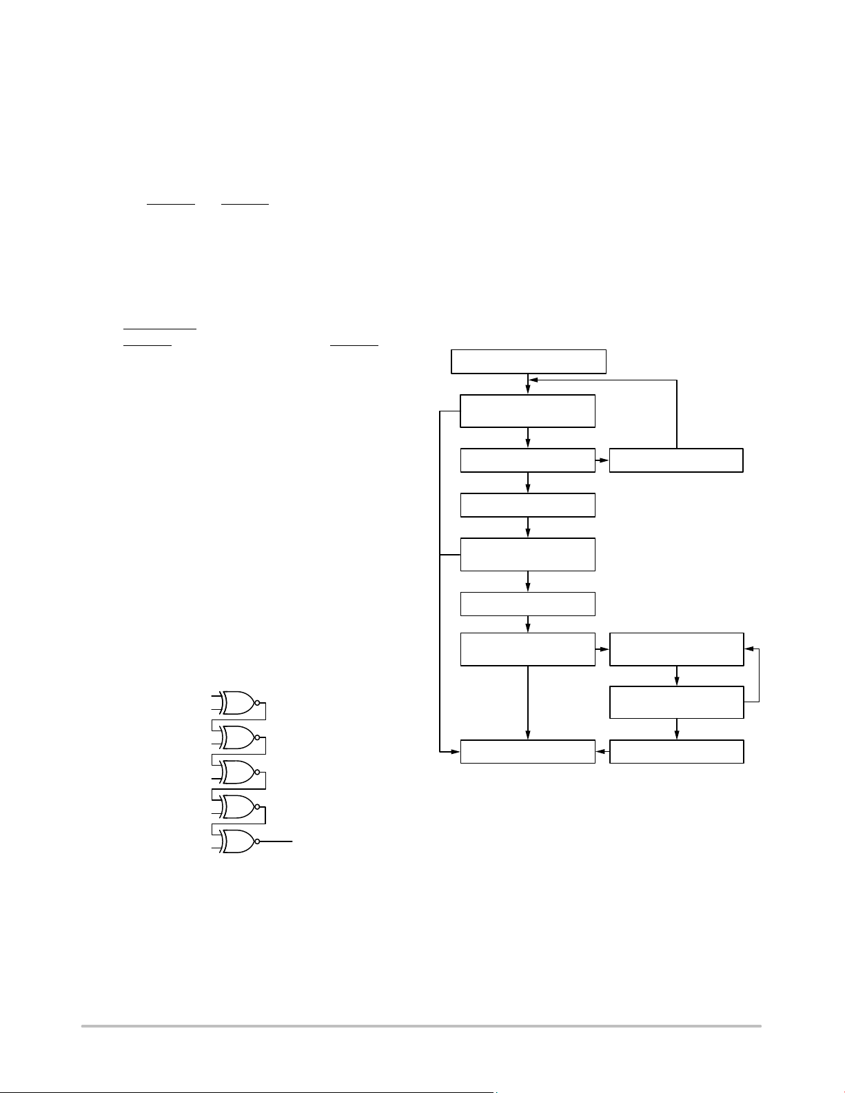
ADT7473
Sleep States
The ADT7473/ADT7473−1 has been specifically
designed to operate from a 3.3 V STBY supply. In computers
that support S3 and S5 states, the core voltage of the
processor is lowered in these states. If using the dynamic
T
mode, lowering the core voltage of the processor
MIN
changes the CPU temperature and the dynamics of the
system under dynamic T
monitoring THERM
, the THERM timer should be disabled
control. Likewise, when
MIN
during these states.
Dynamic T
VCCPLO = 1
When the V
Control Register 1 (0X36) Bit [1]
MIN
voltage drops below the V
CCP
low limit,
CCP
the following occurs:
1. Status Bit 1 (V
2. SMBALERT
3. THERM
monitoring is disabled. The THERM
) in Status Register 1 is set.
CCP
is generated, if enabled.
timer should hold its value prior to the S3 or S5
state.
4. Dynamic T
T
from being adjusted due to an S3 or S5 state.
MIN
control is disabled. This prevents
MIN
5. The ADT7473/ADT7473−1 is prevented from
entering the shutdown state.
Once the core voltage, V
, goes above the V
CCP
CCP
low
limit, everything is re−enabled, and the system resumes
normal operation.
of the default registers after the ADT74731 is addressed via
any valid SMBus transaction.
If V
goes high (the system processor power rail is
CC
powered up), a fail−safe timer begins to count down. If the
ADT7473 is not addressed by any valid SMBus transactions
before the fail−safe timeout (4.6 seconds) lapses, the
ADT7473 drives the fans to full speed. If the ADT7473 is
addressed by a valid SMBus transaction after this point, the
fans stop, and the ADT7473 assumes its default settings and
begins normal operation.
If V
goes high (the system processor power rail is
CCP
powered up), then a fail−safe timer begins to count down. If
the ADT7473 is addressed by a valid SMBus transaction
before the fail−safe timeout (4.6 seconds) lapses, then the
ADT7473 operates normally, assuming the functionality of
all the default registers. See the flow chart in Figure 46.
ADT7473/ADT7473−1 IS POWERED UP
HAS THE ADT7473/ADT7473−1
BEEN ACCESSED BY A VALID
Y
SMBus TRANSACTION?
N
ABOVE 0.75V? CHECK V
IS V
CCP
Y
START FAIL−SAFE TIMER
N
CCP
XNOR Tree Test Mode
The ADT7473/ADT7473−1 includes an XNOR tree test
mode. This mode is useful for in−circuit test equipment at
board−level testing. By applying stimulus to the pins
included in the XNOR tree, it is possible to detect opens or
shorts on the system board.
Figure 45 shows the signals that are exercised in the
XNOR tree test mode. The XNOR tree test is invoked by
setting Bit 0 (XEN) of the XNOR tree test enable register
(0x6F).
TACH1
TACH2
TACH3
TACH4
PWM2
PWM3
PWM1/XTO
Figure 45. XNOR Tree Test
Power−On Default
When the ADT7473 is powered up, it polls the V
CCP
input. By default, the ADT7473−1 powers up with fans
running, eliminating the need for polling of V
If V
stays below 0.75 V (the system CPU power rail
CCP
CCP
.
is not powered up), the ADT7473 assumes the functionality
HAS THE ADT7473/ADT7473−1
BEEN ACCESSED BY A VALID
Y
SMBus TRANSACTION?
N
FAIL−SAFE TIMER ELAPSES
AFTER THE FAIL−SAFE TIMEOUT
HAS THE ADT7473/ADT7473−1
BEEN ACCESSED BY A VALID
SMBus TRANSACTION?
Y
START UP THE
ADT7473/ADT7473−1 NORMALLY
N
RUNS THE FANS
TO FULL SPEED
HAS THE ADT7473/ADT7473−1
BEEN ACCESSED BY A VALID
SMBus TRANSACTION?
SWITCH OFF FANS
Y
N
Figure 46. Power−On Flow Chart
Programming the Automatic Fan Speed Control Loop
To understand the automatic fan speed control loop, it is
strongly recommended to use the ADT7473/ADT7473−1
evaluation board and software while reading this section.
This section provides the system designer with an
understanding of the automatic fan control loop, and
provides step−by−step guidance on effectively evaluating
and selecting critical system parameters. To optimize the
system characteristics, the designer needs to consider the
system configuration, including the number of fans, where
they are located, and what temperatures are measured in the
particular system.
http://onsemi.com
30
Page 31
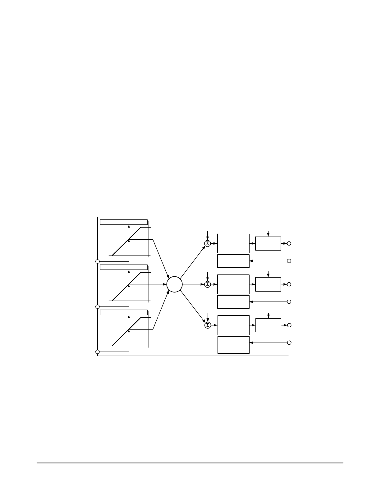
ADT7473
The mechanical or thermal engineer who is tasked with
the system thermal characterization should also be involved
at the beginning of the process.
Automatic Fan Control Overview
The ADT7473/ADT7473−1 can automatically control the
speed of fans based on the measured temperature. This is
done independently of CPU intervention once initial
parameters are set up.
The ADT7473/ADT7473−1 has a local temperature
sensor and two remote temperature channels that can be
connected to a CPU on−chip thermal diode (available on
Intel Pentium class CPUs and other CPUs). These three
temperature channels can be used as the basis for automatic
fan speed control to drive fans using PWM.
Automatic fan speed control reduces acoustic noise by
optimizing fan speed according to accurately measured
temperature. Reducing fan speed can also decrease system
current consumption. The automatic fan speed control mode
is very flexible due to the number of programmable
parameters, including T
T
values for a temperature channel and, therefore, for
RANGE
MIN
and T
RANGE
. The T
MIN
and
a given fan, are critical because they define the thermal
characteristics of the system. The thermal validation of the
system is one of the most important steps in the design
process, so these values should be selected carefully.
Figure 47 gives a top−level overview of the automatic fan
control circuitry on the ADT7473/ADT7473−1. From a
systems−level perspective, up to three system temperatures
can be monitored and used to control three PWM outputs.
The three PWM outputs can be used to control up to four
fans. The ADT7473/ADT7473−1 allows the speed of four
fans to be monitored. Each temperature channel has a
thermal calibration block, allowing the designer to
individually configure the thermal characteristics of each
temperature channel. For example, a designer can decide to
run the CPU fan when CPU temperature increases above
60°C, and a chassis fan when the local temperature increases
above 45°C. At this stage, the designer has not assigned
these thermal calibration settings to a particular fan drive
(PWM) channel. The right side of Figure 47 shows controls
that are fan−specific. The designer has individual control
over parameters such as minimum PWM duty cycle, fan
speed failure thresholds, and even ramp control of the PWM
outputs. Automatic fan control, then, ultimately allows
graceful fan speed changes that are less perceptible to the
system user.
REMOTE 1
TEMP
LOCAL
TEMP
REMOTE 2
TEMP
THERMAL CALIBRATION
T
MIN
THERMAL CALIBRATION
T
MIN
THERMAL CALIBRATION
T
MIN
T
RANGE
T
RANGE
T
RANGE
Figure 47. Automatic Fan Control Block Diagram
100%
0%
100%
0%
100%
0%
MUX
PWM
MIN
PWM
MIN
PWM
MIN
RAMP
CONTROL
(ACOUSTIC
ENHANCEMENT)
TACHOMETER 1
MEASUREMENT
RAMP
CONTROL
(ACOUSTIC
ENHANCEMENT)
TACHOMETER 2
MEASUREMENT
RAMP
CONTROL
(ACOUSTIC
ENHANCEMENT)
TACHOMETER 3
AND 4
MEASUREMENT
PWM
CONFIG
PWM
GENERATOR
PWM
CONFIG
PWM
GENERATOR
PWM
CONFIG
PWM
GENERATOR
PWM1
TACH1
PWM2
TACH2
PWM3
TACH3
http://onsemi.com
31
Page 32
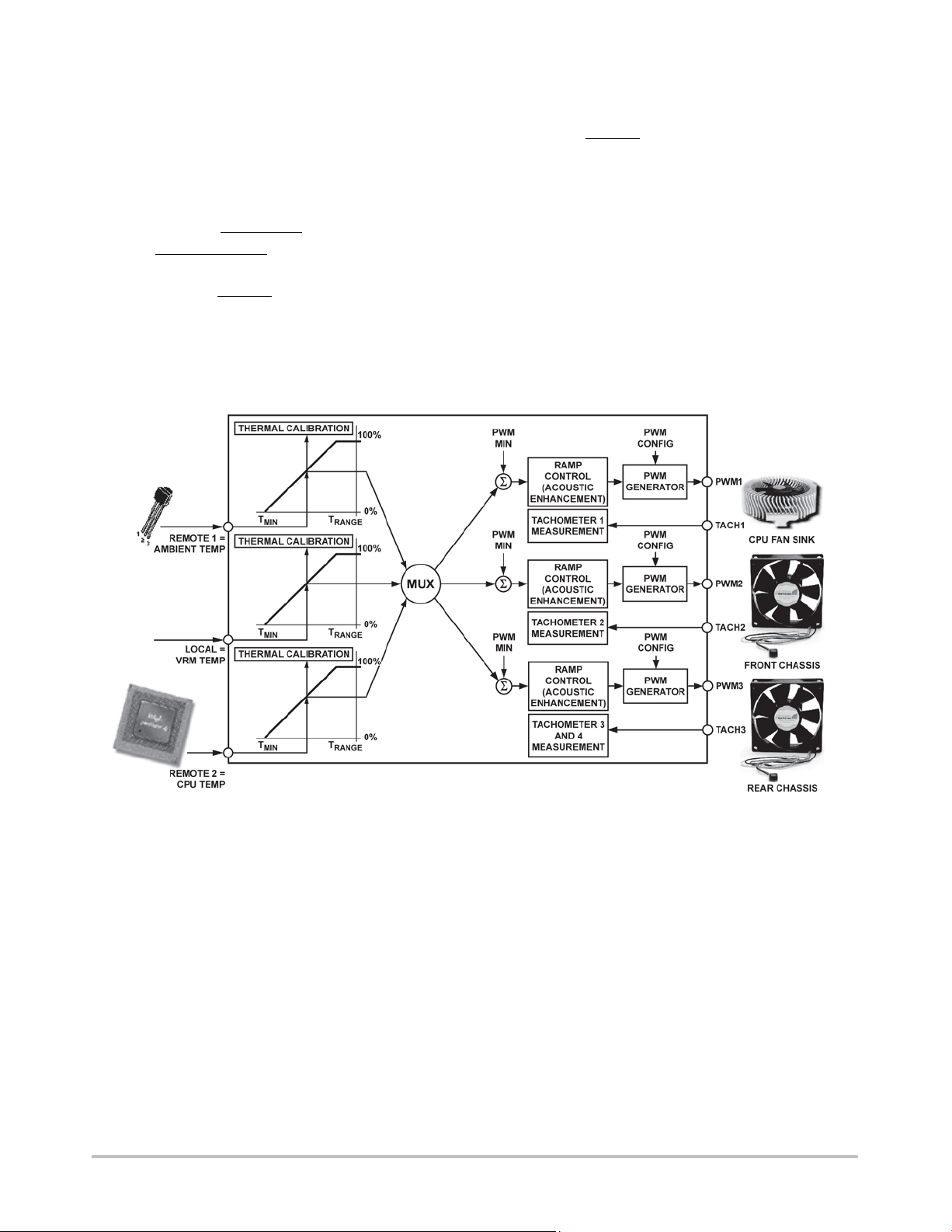
ADT7473
Step 1: Hardware Configuration
During system design, the motherboard sensing and
control capabilities should be addressed early in the design
stages. Decisions about how these capabilities are used
should involve the system thermal/mechanical engineer.
Consider the following questions:
1. What ADT7473/ADT7473−1 functionality will be
used?
• PWM2 or SMBALERT for ADT7473?
• THERM_LATCH or PWM2 for ADT7473−1?
• TACH4 fan speed measurement or over−
temperature THERM
ADT7473−1 offers multifunctional pins that can
be reconfigured to suit different system
requirements and physical layouts. These
multifunction pins are software programmable.
function? The ADT7473/
2. How many fans will be supported in the system,
three or four? This influences the choice of
whether to use the TACH4 pin or to reconfigure it
for the THERM
3. Is the CPU fan to be controlled using the
ADT7473/ADT7473−1 or will it run at full speed
100% of the time?
If run at full speed, 100% of the time, this frees up
a PWM output, but the system is louder.
4. Where will the ADT7473/ADT7473−1 be
physically located in the system?
This influences the assignment of the temperature
measurement channels to particular system thermal zones.
For example, locating the ADT7473/ADT7473−1 close to
the VRM controller circuitry allows the VRM temperature
to be monitored using the local temperature channel.
function.
Figure 48. Hardware Configuration Example
http://onsemi.com
32
Page 33
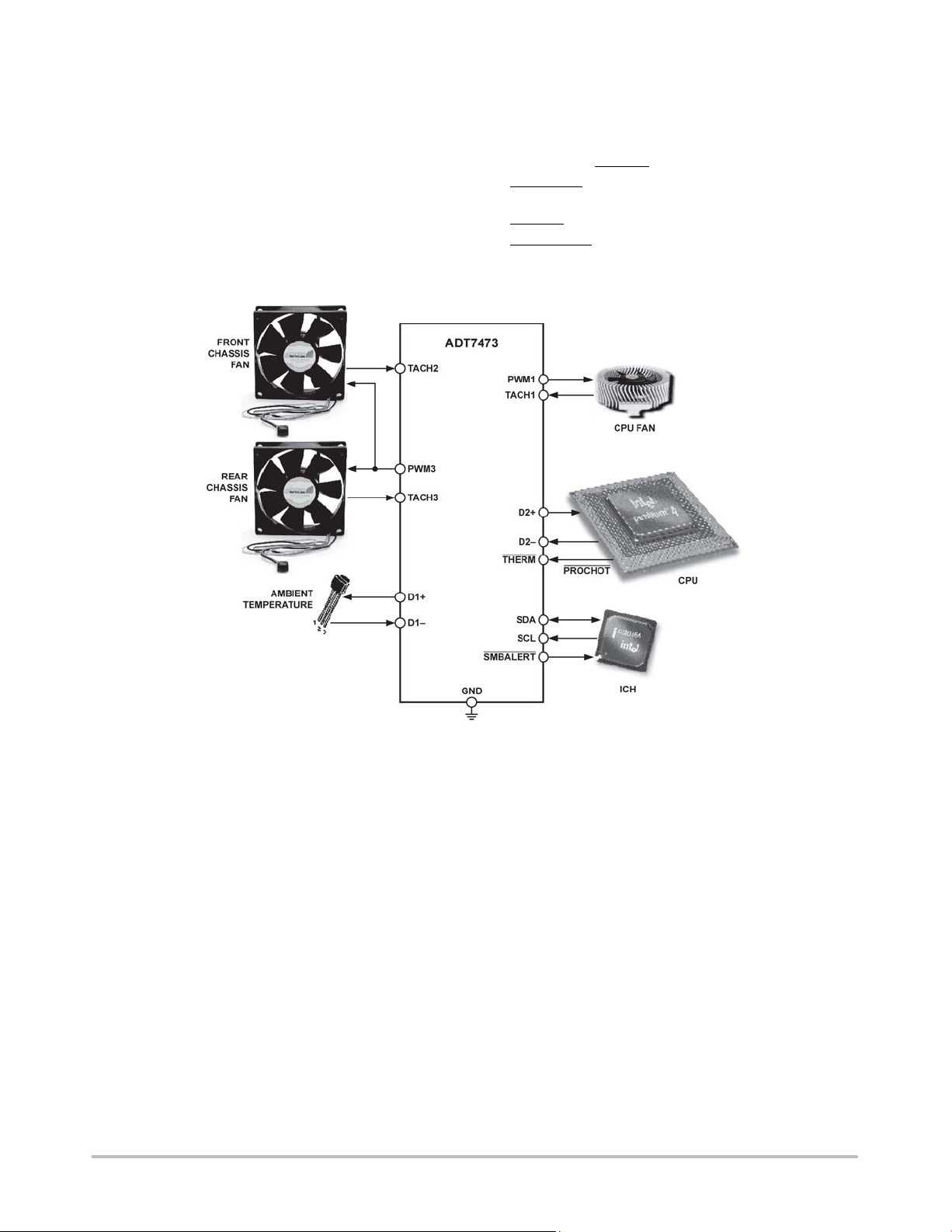
ADT7473
Recommended Implementation 1
Configuring the ADT7473, as in Figure 49 provides the
system designer with the following features:
• Two PWM outputs for fan control of up to three fans.
(The front and rear chassis fans are connected in
parallel.)
• Three TACH fan speed measurement inputs.
• V
measured internally through Pin 4.
CC
• CPU core voltage measurement (V
CORE
).
• VRM temperature using local temperature sensor.
• CPU temperature measured using the Remote 1
temperature channel.
• Ambient temperature measured through the Remote 2
temperature channel.
• Bidirectional THERM pin allows the monitoring of
PROCHOT
for example, or can be used as an overtemperature
THERM
output from an Intel Pentium 4 processor,
output.
• SMBALERT system interrupt output.
Figure 49. Recommended Implementation 1
http://onsemi.com
33
Page 34
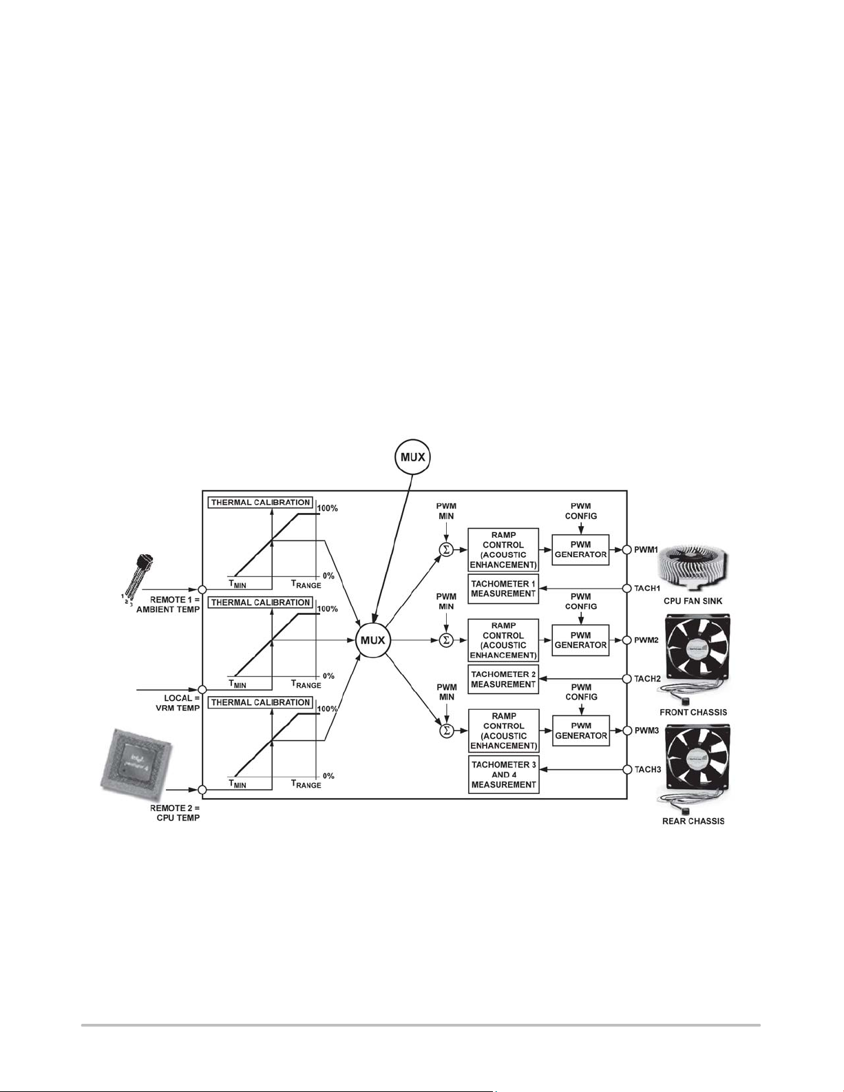
ADT7473
Step 2: Configuring the Mux
After the system hardware configuration is determined,
the fans can be assigned to particular temperature channels.
Not only can fans be assigned to individual channels, but the
behavior of the fans is also configurable. For example, fans
can be run under automatic fan control, manually (under
software control), or at the fastest speed calculated by
multiple temperature channels. The mux is the bridge
between temperature measurement channels and the three
PWM outputs.
Bits [7:5] (BHVR) of Register 0x5C, Register 0x5D, and
Register 0x5E (PWM configuration registers) control the
behavior of the fans connected to the PWM1, PWM2, and
PWM3 outputs. The values selected for these bits determine
how the mux connects a temperature measurement channel
to a PWM output.
Automatic Fan Control Mux Options
Bits [7:5] (BHVR), Register 0x5C, Register 0x5D, Register
0x5E.
000 = Remote 1 temperature controls PWMx
001 = Local temperature controls PWMx
010 = Remote 2 temperature controls PWMx
101 = Fastest speed calculated by local and Remote 2
temperature controls PWMx
110 = Fastest speed calculated by all three
temperature channel controls PWMx
The fastest speed calculated options pertain to controlling
one PWM output based on multiple temperature channels.
The thermal characteristics of the three temperature zones
can be set to drive a single fan. An example is the fan turning
on when Remote 1 temperature exceeds 60°C, or if the local
temperature exceeds 45°C.
Other Mux Options
Bits [7:5] (BHVR), Register 0x5C, Register 0x5D, Register
0x5E.
011 = PWMx runs full speed (default for
ADT7473−1)
100 = PWMx disabled (default for ADT7473)
111 = manual mode
In normal mode, PWMx runs under software control. In
this mode, PWM duty cycle registers (Register 0x30 to
Register 0x32) are writable and control the PWM outputs.
Figure 50. Assigning Temperature Channels to Fan Channels
http://onsemi.com
34
Page 35
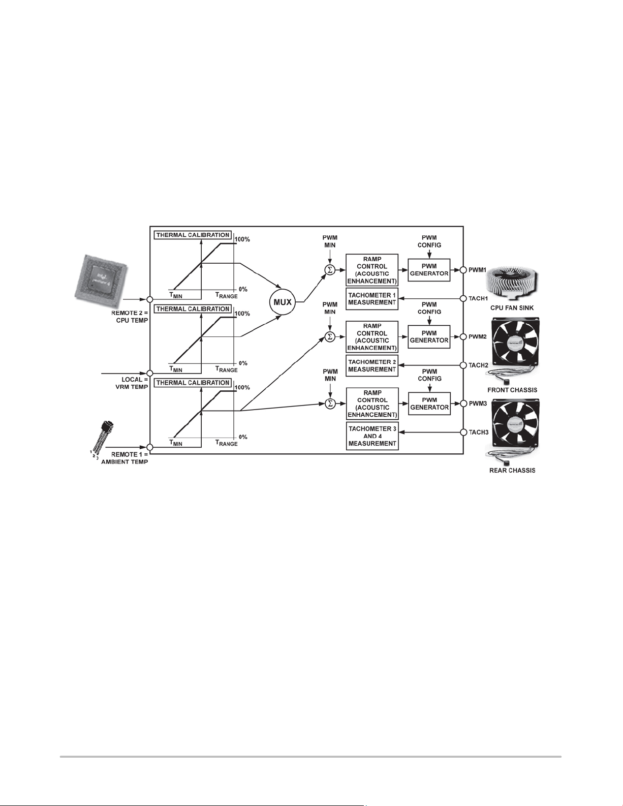
ADT7473
Mux Configuration Example
This is an example of how to configure the mux in a
system using the ADT7473/ADT7473−1 to control three
fans. The CPU fan sink is controlled by PWM1, the front
chassis fan is controlled by PWM2, and the rear chassis fan
is controlled by PWM3. The mux is configured for the
following fan control behaviors:
• PWM1 (CPU fan sink) is controlled by the fastest speed
calculated by the local (VRM temperature) and
Remote 2 (processor) temperature. In this case, the
CPU fan sink is also used to cool the VRM.
• PWM2 (front chassis fan) is controlled by the Remote 1
temperature (ambient).
• PWM3 (rear chassis fan) is controlled by the Remote 1
temperature (ambient).
Example Mux Settings
Bits [7:5] (BHVR), PWM1 Configuration Register (0x5C)
101 = Fastest speed calculated by local and Remote 2
temperature controls PWM1
Bits [7:5] (BHVR), PWM2 Configuration Register (0x5D)
000 = Remote 1 temperature controls PWM2
Bits [7:5] (BHVR), PWM3 Configuration Register (0x5E)
000 = Remote 1 temperature controls PWM3
These settings configure the mux, as shown in Figure 51.
Figure 51. Mux Configuration Example
Step 3: T
T
MIN
Settings for Thermal Calibration Channels
MIN
is the temperature at which the fans start to turn on
under automatic fan control. The speed at which the fan runs
at T
is programmed later. The T
MIN
values chosen are
MIN
temperature channel specific, for example, 25°C for
ambient channel, 30°C for VRM temperature, and 40°C for
processor temperature.
T
is an 8−bit value, either twos complement or Offset
MIN
64, that can be programmed in 1°C increments. A T
MIN
register is associated with each temperature measurement
channel: Remote 1 local and Remote 2 temperature. Once
the T
value is exceeded, the fan turns on and runs at the
MIN
minimum PWM duty cycle. The fan turns off once the
temperature drops below T
MIN
− T
HYST
.
To overcome fan inertia, the fan is spun up until two valid
TACH rising edges are counted. See the Fan Startup
Timeout section for more details. In some cases, primarily
for psycho−acoustic reasons, it is desirable that the fan never
switches off below T
. Bits [7:5] of Enhanced Acoustics
MIN
Register 1 (0x62), when set, can keep the fans running at the
http://onsemi.com
PWM minimum duty cycle, if the temperature falls below
.
T
MIN
T
Registers
MIN
Register 0x67, Remote 1 Temperature T
Register 0x68, Local Temperature T
Register 0x69, Remote 2 Temperature T
Enhanced Acoustics Register 1 (0x62)
= 0x9A (90°C)
MIN
= 0x9A (90°C)
MIN
= 0x9A (90°C)
MIN
Bit 7 (MIN3) = 0, PWM3 is off (0% PWM duty cycle) when
temperature is below T
MIN
− T
HYST
.
Bit 7 (MIN3) = 1, PWM3 runs at PWM3 minimum duty
cycle below T
MIN
− T
HYST
.
Bit 6 (MIN2) = 0, PWM2 is off (0% PWM duty cycle) when
temperature is below T
MIN
− T
HYST
.
Bit 6 (MIN2) = 1, PWM2 runs at PWM2 minimum duty
cycle below T
MIN
− T
HYST
.
Bit 5 (MIN1) = 0, PWM1 is off (0% PWM duty cycle) when
temperature is below T
MIN
− T
HYST
.
Bit 5 (MIN1) = 1, PWM1 runs at PWM1 minimum duty
cycle below T
35
MIN
− T
HYST
.
Page 36
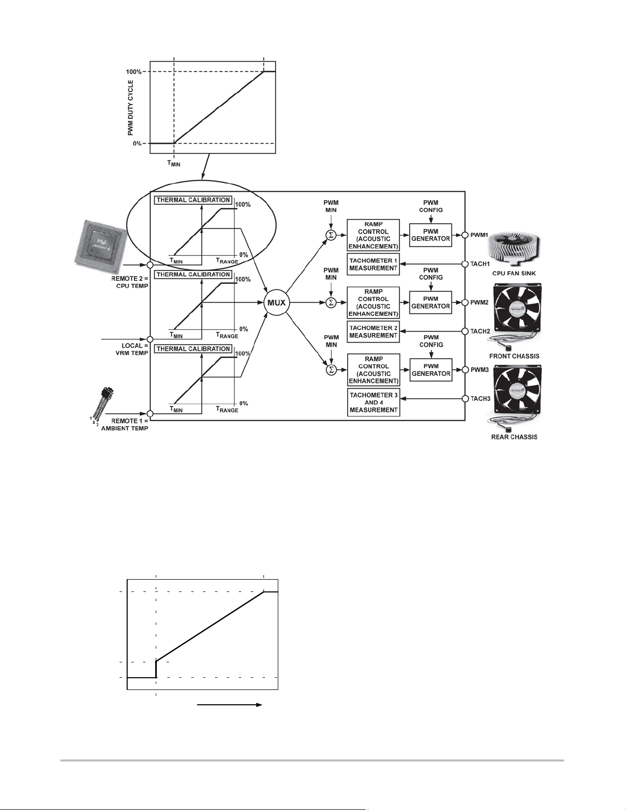
ADT7473
Figure 52. Understanding the T
Step 4: PWM
PWM
MIN
for Each PWM (Fan) Output
MIN
is the minimum PWM duty cycle at which each
fan in the system runs. It is also the start speed for each fan
under automatic fan control once the temperature rises
above T
benefit, PWM
Depending on the fan used, the PWM
(see Figure 53). For maximum system acoustic
MIN
should be set as low as possible.
MIN
setting is usually
MIN
in the 20% to 33% duty cycle range. This value can be found
through fan validation.
100%
PWM DUTY CYCLE
PWM
MIN
0%
T
Figure 53. PWM
PWM Duty Cycle
MIN
MIN
TEMPERATURE
Determines Minimum
Parameter
MIN
More than one PWM output can be controlled from a
single temperature measurement channel. For example,
Remote 1 temperature can control PWM1 and PWM2
outputs. If two different fans are used on PWM1 and PWM2,
the fan characteristics can be set up differently. As a result,
Fan 1 driven by PWM1 can have a different PWM
MIN
value
than that of Fan 2 connected to PWM2. Figure 54 illustrates
this as PWM1
cycle of 20%, while PWM2
(front fan) is turned on at a minimum duty
MIN
(rear fan) turns on at a
MIN
minimum of 40% duty cycle. However, both fans turn on at
exactly the same temperature, defined by T
MIN
.
http://onsemi.com
36
Page 37
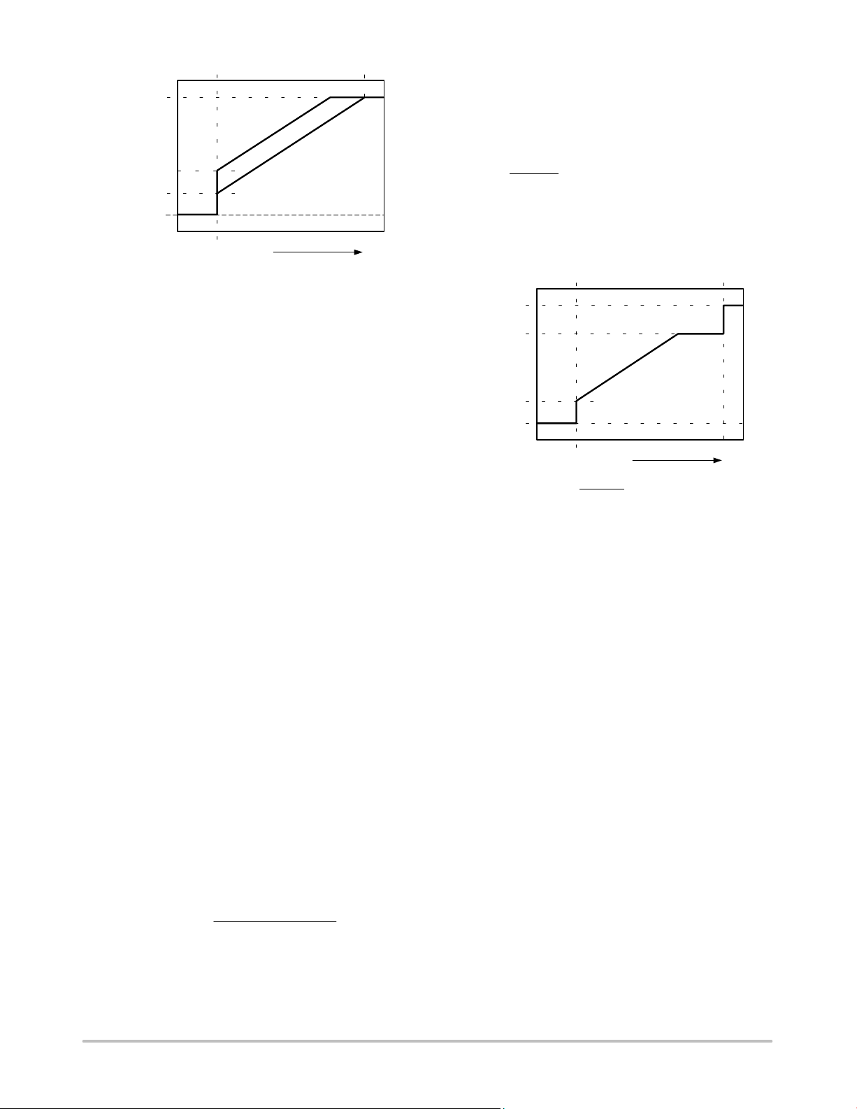
ADT7473
100%
PWM2
PWM2
MIN
PWM DUTY CYCLE
PWM1
MIN
0%
T
MIN
PWM1
TEMPERATURE
Figure 54. Operating Two Different Fans from a
Single Temperature Channel
Programming the PWM
The PWM
registers are 8−bit registers that allow the
MIN
Registers
MIN
minimum PWM duty cycle for each output to be configured
anywhere from 0% to 100%. This allows the minimum
PWM duty cycle to be set in steps of 0.39%.
The value to be programmed into the PWM
register is
MIN
given by:
Value (decimal) = PWM
Example 1
MIN
/0.39
For a minimum PWM duty cycle of 50%
Value (decimal) = 50/0.39 = 128 (decimal)
Value = 128 (decimal) or 80 (hex)
Example 2
For a minimum PWM duty cycle of 33%
Value (decimal) = 33/0.39 = 85 (decimal)
Value = 85 (decimal) or 54 (hex)
PWM
Registers
MIN
Register 0x64, PWM1 Minimum Duty Cycle = 0x80 (50%
default)
Register 0x65, PWM2 Minimum Duty Cycle = 0x80 (50%
default)
Register 0x66, PWM3 Minimum Duty Cycle = 0x80 (50%
default)
Note on Fan Speed and PWM Duty Cycle
The PWM duty cycle does not directly correlate to fan
speed in RPM. Running a fan at 33% PWM duty cycle does
not equate to running the fan at 33% speed. Driving a fan at
33% PWM duty cycle actually runs the fan at closer to 50%
of its full speed. This is because fan speed in %RPM
generally relates to the square root of PWM duty cycle.
Given a PWM square wave as the drive signal, fan speed in
RPM approximates to:
% fanspeed + PWM duty cycle 10
Ǹ
(eq. 4)
Step 5: PWM
PWM
MAX
for PWM (Fan) Outputs
MAX
is the maximum duty cycle at which each fan
in the system runs under the automatic fan speed control
loop. For maximum system acoustic benefit, PWM
MAX
should be as low as possible, but should be capable of
maintaining the processor temperature limit at an acceptable
level. If the THERM
temperature limit is exceeded, the fans
are still boosted to 100% for fail−safe cooling (see
Figure 55).
There is a PWM
limit for each fan channel. The
MAX
default value of this register is 0xFF and thus has no effect
unless it is programmed.
100%
PWM
MAX
PWM DUTY CYCLE
PWM
MIN
0%
T
Figure 55. PWM
Determines Maximum PWM Duty
MAX
Cycle Below the THERM
Programming the PWM
The PWM
registers are 8−bit registers that allow the
MAX
MIN
MAX
TEMPERATURE
Temperature Limit
Registers
maximum PWM duty cycle for each output to be configured
anywhere from 0% to 100%. This allows the maximum
PWM duty cycle to be set in steps of 0.39%.
The value to be programmed into the PWM
MAX
register
is given by:
Value (decimal) = PWM
Example 1
MAX
/0.39
For a maximum PWM duty cycle of 50%
Value (decimal) = 50/0.39 = 128 (decimal)
Value = 128 (decimal) or 80 (hex)
Example 2
For a minimum PWM duty cycle of 75%
Value (decimal) = 75/0.39 = 85 (decimal)
Value = 192 (decimal) or C0 (hex)
PWM
Registers
MAX
Register 0x38, PWM1 Maximum Duty Cycle = 0xFF
(100% default)
Register 0x39, PWM2 Maximum Duty Cycle = 0xFF
(100% default)
Register 0x3A, PWM3 Maximum Duty Cycle = 0xFF
(100% default)
See the Note on Fan Speed and PWM Duty Cycle section.
http://onsemi.com
37
Page 38
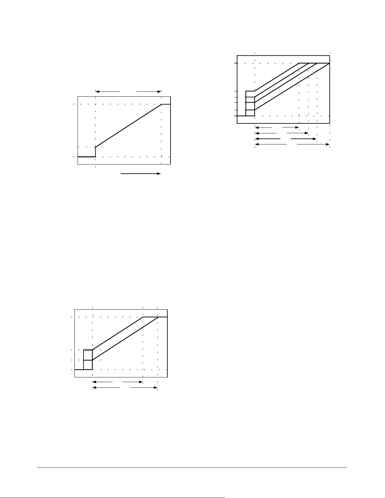
ADT7473
Step 6: T
T
RANGE
fan control occurs once the programmed T
is exceeded. T
value, that is, a T
PWM
MIN
effective T
PWM DUTY CYCLE
PWM
Figure 56. T
The T
for Temperature Channels
RANGE
is the range of temperature over which automatic
temperature
MIN
is a temperature slope, not an arbitrary
RANGE
of 40°C holds true only for
RANGE
= 33%. If PWM
changes. Refer to Figure 56.
RANGE
100%
MIN
0%
T
Parameter Affects Cooling Slope
RANGE
or fan control slope is determined by the
RANGE
is increased or decreased, the
MIN
T
RANGE
MIN
TEMPERATURE
following procedure:
1. Determine the maximum operating temperature for
that channel (for example, 70°C).
2. Determine experimentally the fan speed (PWM
duty cycle value) that does not exceed the
temperature at the worst−case operating points (for
example, 70°C is reached when the fans are
running at 50% PWM duty cycle).
3. Determine the slope of the required control loop to
meet these requirements.
4. Graphically program and visualize this
functionality using the ADT7473/ADT7473−1
evaluation software.
Figure 57 shows how adjusting PWM
100%
50%
PWM DUTY CYCLE
33%
0%
305C
T
Figure 57. Adjusting PWM
T
PWM
is implemented as a slope, which means that as
RANGE
is changed, T
MIN
MIN
RANGE
405C
MIN
changes, but the actual slope
remains the same. The higher the PWM
smaller the effective T
, that is, the fan reaches full
RANGE
affects T
MIN
Affects T
MIN
RANGE
RANGE
value, the
speed (100%) at a lower temperature. Figure 58 shows how
increasing PWM
100%
50%
33%
25%
PWM DUTY CYCLE
10%
0%
Figure 58. Increasing PWM
For a given T
fan runs at full speed for different PWM
changes the effective T
MIN
305C
405C
455C
T
MIN
T
RANGE
value, the temperature at which the
RANGE
545C
Changes Effective
MIN
MIN
easily calculated as follows:
T
MAX
= T
+ (Max DC − Min DC) x T
MIN
where:
is the temperature at which the fan runs full speed.
T
MAX
is the temperature at which the fan turns on.
T
MIN
Max DC is the maximum duty cycle (100%) = 255 decimal.
Min DC is equal to PWM
T
Example 1
is the duty PWM duty cycle vs. temperature slope.
RANGE
Calculate T, given that T
.
PWM
T
MAX
T
MAX
T
MAX
T
MAX
Example 2
= 10% duty cycle = 26 (decimal).
MIN
= T
MIN
= 30°C + (100% − 10%) x 40°C/170
= 30°C + (255 − 26) x 40°C/170
= 84°C (effective T
Calculate T
40°C, and PWM
= T
T
T
T
T
MAX
MAX
MAX
MAX
MIN
= 30°C + (100% − 25%) x 40°C/170
= 30°C + (255 − 64) x 40°C/170
= 75°C (effective T
Example 3
Calculate T
40°C, and PWM
= T
T
T
T
T
MAX
MAX
MAX
MAX
MIN
= 30°C + (100% − 33%) x 40°C/170
= 30°C + (255 − 85) x 40°C/170
= 70°C (effective T
+ (Max DC − Min DC) x T
, given that T
MAX
= 25% duty cycle = 64 (decimal).
MIN
+ (Max DC − Min DC) x T
, given that T
MAX
= 33% duty cycle = 85 (decimal).
MIN
+ (Max DC − Min DC) x T
.
MIN
= 30°C, T
MIN
RANGE
RANGE
RANGE
RANGE
= 54°C)
= 30°C, T
MIN
= 45°C)
= 30°C, T
MIN
= 40°C)
RANGE
RANGE
RANGE
.
RANGE
values can be
/170
RANGE
= 40°C, and
/170
=
RANGE
/170
=
RANGE
/170
http://onsemi.com
38
Page 39
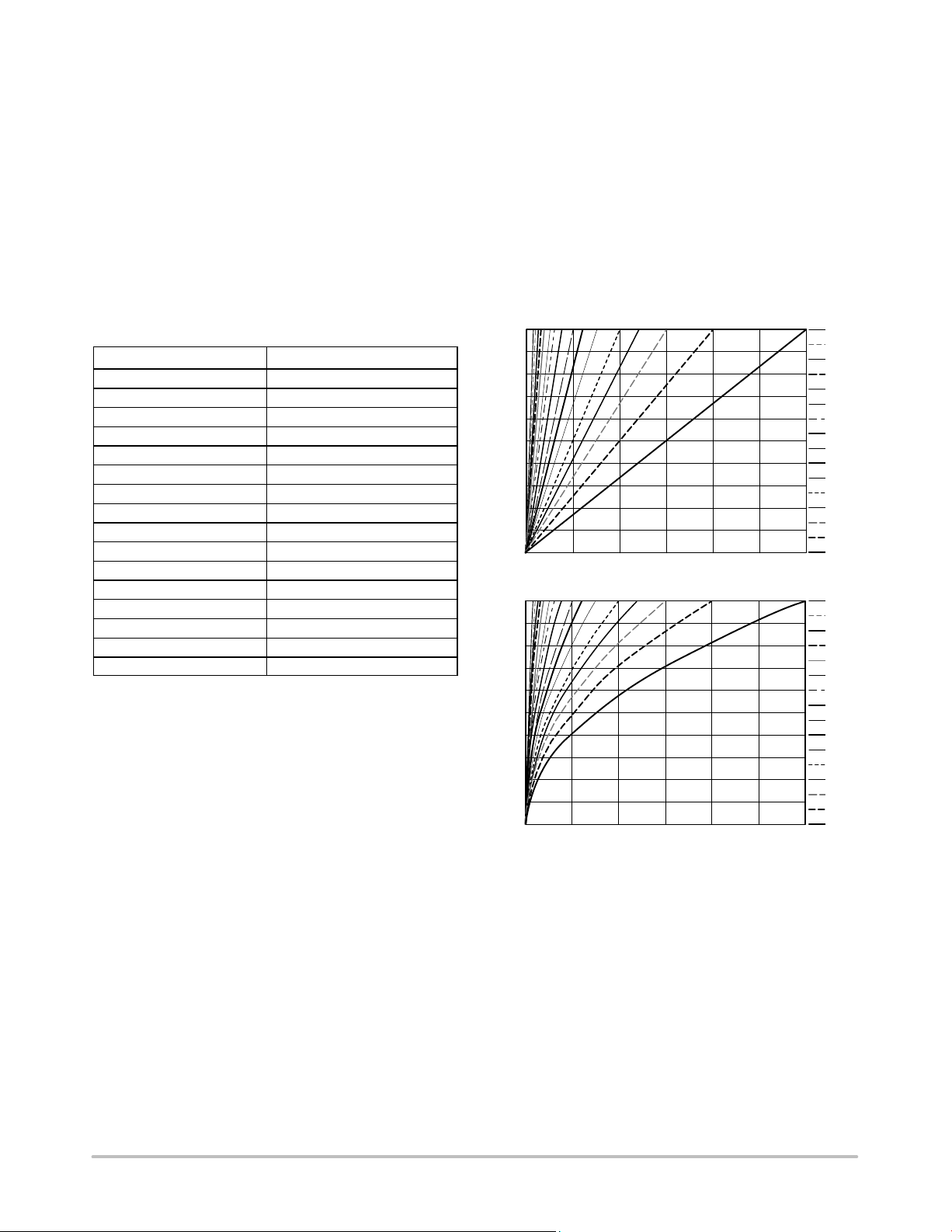
ADT7473
Example 4
Calculate T
40°C, and PWM
T
= T
MAX
T
MAX
T
MAX
T
MAX
Selecting a T
The T
MIN
= 30°C + (100% − 50%) x 40°C/170
= 30°C + (255 − 128) x 40°C/170
= 60°C (effective T
RANGE
, given that T
MAX
= 50% duty cycle = 128 (decimal).
MIN
+ (Max DC − Min DC) x T
RANGE
Slope
RANGE
= 30°C, T
MIN
= 30°C)
RANGE
RANGE
/170
value can be selected for each temperature
=
channel: Remote 1, local, and Remote 2. Bits [7:4]
(T
T
RANGE
Table 13. Selecting a T
1. Register 0x5F configures Remote 1 T
Summary of T
) of Register 0x5F to Register 0x61 define the
RANGE
value for each temperature channel.
Value
RANGE
Bits [7:4] (Note 1) T
0000 2
0001 2.5
0010 3.33
0011 4
0100 5
0101 6.67
0110 8
0111 10
1000 13.33
1001 16
1010 20
1011 26.67
1100 32 (default)
1101 40
1110 53.33
1111 80
configures local T
.
T
RANGE
RANGE
; Register 0x61 configures Remote 2
RANGE
Function
RANGE
RANGE
(5C)
; Register 0x60
When using the automatic fan control function, the
temperature at which the fan reaches full speed can be
calculated by:
T
+ T
MAX
Equation 1 holds true only when PWM
MIN
) T
TRANGE
MIN
(eq. 5)
is equal to 33%
PWM duty cycle.
Increasing or decreasing PWM
T
, although the fan control still follows the same
RANGE
changes the effective
MIN
PWM duty cycle to temperature slope. The effective
T
for different PWM
RANGE
values can be calculated
MIN
using Equation 6.
See the Note on Fan Speed and PWM Duty Cycle section.
Figure 59 shows PWM duty cycle vs. temperature for each
T
setting. The lower graph shows how each T
RANGE
RANGE
setting affects fan speed vs. temperature. As indicated by the
graph, the effect on fan speed is nonlinear.
The graphs in Figure 59 assume the fan starts from 0%
PWM duty cycle. Clearly, the minimum PWM duty cycle,
PWM
, needs to be factored in to see how the loop
MIN
actually performs in the system. Figure 60 shows how
T
is affected when the PWM
RANGE
value is set to 20%.
MIN
It can be seen that the fan actually runs at about 45% fan
speed when the temperature exceeds T
100
90
80
70
60
50
40
30
PWM DUTY CYCLE (%)
20
10
0
0 20 40 60 80 100 120
100
90
80
70
60
50
40
30
FAN SPEED (% OF MAX)
20
10
0
0 20406080100120
Figure 59. T
TEMPERATURE ABOVE T
TEMPERATURE ABOVE T
vs. Actual Fan Speed Profile
RANGE
MIN
MIN
MIN
.
25C
2.55C
3.335C
45C
55C
6.675C
85C
105C
13.35C
165C
205C
26.65C
325C
405C
53.35C
805C
25C
2.55C
3.335C
45C
55C
6.675C
85C
105C
13.35C
165C
205C
26.65C
325C
405C
53.35C
805C
T
MAX
+ T
)ǒMax DC * Min DCǓ T
MIN
where (Max DC − Min DC) x T
T
RANGE
value.
TRANGE
/170 is the effective
RANGE
ń170
(eq. 6)
http://onsemi.com
39
Page 40
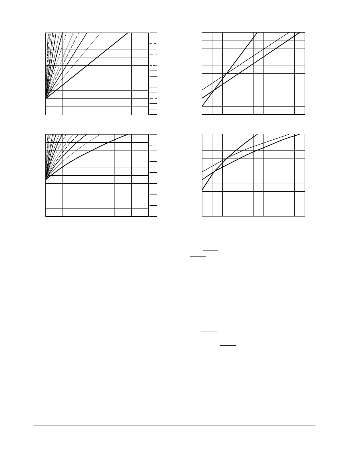
ADT7473
C
C
C
C
C
C
C
C
C
C
100
90
80
70
60
50
40
30
PWM DUTY CYCLE (%)
20
10
0
0 20 40 60 80 100 120
100
90
80
70
60
50
40
30
FAN SPEED (% OF MAX)
20
10
0
0 20 40 60 80 100 120
TEMPERATURE ABOVE T
TEMPERATURE ABOVE T
MIN
MIN
25C
2.55C
3.335
45C
55C
6.675
85C
105C
13.35
165C
205C
26.65
325C
405C
53.35
805C
25C
2.55C
3.335
45C
55C
6.675
85C
105C
13.35
165C
205C
26.65
325C
405C
53.35
805C
100
90
80
70
60
50
40
30
PWM DUTY CYCLE (%)
20
10
0
0 10203040 10050 60 70 80 90
100
90
80
70
60
50
40
30
FAN SPEED (% MAX RPM)
20
10
0
0 10203040 10050 60 70 80 90
TEMPERATURE ABOVE T
TEMPERATURE ABOVE T
MIN
MIN
Figure 60. T
Example: Determining T
and % Fan Speed Slopes with
RANGE
PWM
= 20%
MIN
for Each Temperature
RANGE
Channel
The following example shows how the different T
T
settings can be applied to three different thermal
RANGE
zones. In this example, the following T
T
T
T
= 80°C for ambient temperature
RANGE
= 53.3°C for CPU temperature
RANGE
= 40°C for VRM temperature
RANGE
RANGE
values apply:
MIN
and
This example uses the mux configuration described in the
Step 2: Configuring the Mux section, with the ADT7473/
ADT7473−1 connected as shown in Figure 61. Both CPU
temperature and VRM temperature drive the CPU fan
connected to PWM1.
Ambient temperature drives the front chassis fan and rear
chassis fan connected to PWM2 and PWM3. The front
chassis fan is configured to run at PWM
chassis fan is configured to run at PWM
CPU fan is configured to run at PWM
Note on 4−Wire Fans
The control range for 4−wire fans is much wider than that
= 20%. The rear
MIN
= 30%. The
MIN
= 10%.
MIN
for 3−wire fans. In many cases, 4−wire fans can start with a
PWM drive of as little as 20%.
Figure 61. T
and % Fan Speed Slopes for VRM,
RANGE
Ambient, and CPU Temperature Channels
Step 7: T
T
THERM
for Temperature Channels
THERM
is the absolute maximum temperature allowed
on a temperature channel. When operating above this
temperature, a component such as the CPU or VRM might
be beyond its safe operating limit. When the temperature
measured exceeds T
all fans are driven at 100%
THERM
PWM duty cycle (full speed) to provide critical system
cooling.
The fans remain running at 100% until the temperature
drops below T
− hysteresis, where hysteresis is the
THERM
number programmed into the hysteresis registers (Register
0x6D and Register 0x6E). The default hysteresis value is 4°C.
The T
limit should be considered the maximum
THERM
worst−case operating temperature of the system. Because
exceeding any T
limit runs all fans at 100%, it has
THERM
very negative acoustic effects. Ultimately, this limit should
be set up as a fail−safe, and it should not be exceeded under
normal system operating conditions.
Note that the T
limits are nonmaskable and affect
THERM
the fan speed no matter how the automatic fan control
settings are configured. This allows some flexibility because
a T
hard limit (such as 70°C), can be programmed as T
value can be selected based on its slope, while a
RANGE
MAX
(the
http://onsemi.com
40
Page 41
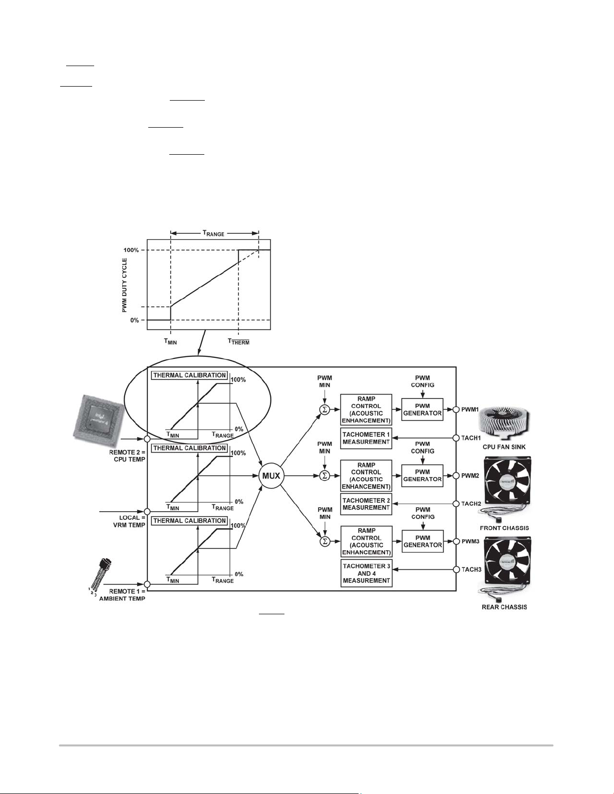
ADT7473
temperature at which the fan reaches full speed) by setting
T
THERM Registers
to that limit (for example, 70°C).
THERM
Register 0x6A, Remote 1 THERM Temperature Limit =
0xA4 (100°C default)
Register 0x6B, Local THERM
Temperature Limit = 0xA4
(100°C default)
Register 0x6C, Remote 2 THERM
Temperature Limit =
0xA4 (100°C default)
Hysteresis Registers
Register 0x6D, Remote 1 Local Temperature Hysteresis
Register
Bits [7:4] Remote 1 temperature hysteresis (4°C default)
Bits [3:0] Local temperature hysteresis (4°C default)
Register 0x6E, Remote 2 Temperature Hysteresis Register
Bits [7:4] Remote 2 temperature hysteresis (4°C default)
Because each hysteresis setting is four bits, hysteresis
values are programmable from 1°C to 15°C. It is not
recommended that hysteresis values be programmed to 0°C,
because this disables hysteresis. In effect, this would cause
the fans to cycle between normal speed and 100% speed,
creating unsettling acoustic noise.
Figure 62. How T
Step 8: T
T
HYST
for Temperature Channels
HYST
is the amount of extra cooling a fan provides after
the temperature measured has dropped back below T
Relates to Automatic Fan Control
THERM
MIN
before the fan turns off. The premise for temperature
hysteresis (T
) is that, without it, the fan would merely
HYST
chatter or cycle on and off regularly whenever temperature
is hovering at about the T
MIN
setting.
http://onsemi.com
The T
value chosen determines the amount of time
HYST
needed for the system to cool down or heat up as the fan turns
on and off. Values of hysteresis are programmable in the
range 1°C to 15°C. Larger values of T
from chattering on and off. The T
HYST
prevent the fans
HYST
default value is set
at 4°C.
41
Page 42
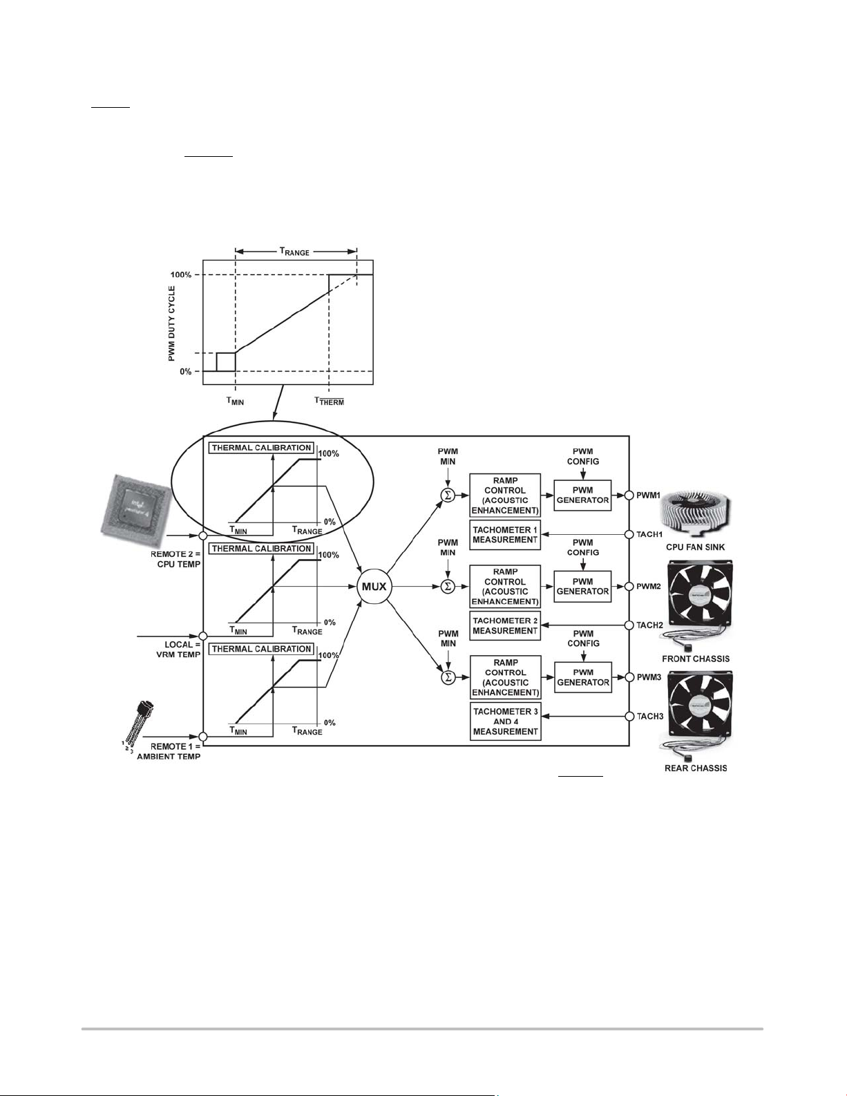
ADT7473
The T
setting applies not only to the temperature
HYST
hysteresis for fan on/off, but the same setting is used for the
T
hysteresis value, described in Step 6: T
THERM
RANGE
for
Temperature Channels section. Therefore, programming
Register 0x6D and Register 0x6E sets the hysteresis for both
fan on/off and the THERM
Hysteresis Registers
function.
Register 0x6D, Remote 1, Local Hysteresis Register
Bits [7:4], Remote 1 temperature hysteresis (4°C default)
Bits [3:0], Local temperature hysteresis (4°C default)
Register 0x6E, Remote 2 Temperature Hysteresis Register
Bits [7:4], Remote 2 temperature hysteresis (4°C default)
In some applications, it is required that fans not turn off
below T
, but remain running at PWM
MIN
. Bits [7:5] of
MIN
the Enhanced Acoustics Register 1 (0x62) allow the fans to
be turned off or to be kept spinning below T
are always on, the T
the temperature drops below T
value has no effect on the fan when
HYST
.
MIN
. If the fans
MIN
Figure 63. The T
Enhanced Acoustics Register 1 (0x62)
Value Applies to Fan On/Off Hysteresis and THERM Hysteresis
HYST
Bit 7 (MIN3) = 0, PWM3 is off (0% PWM duty cycle) when
temperature is below T
MIN
− T
HYST
.
Bit 7 (MIN3) = 1, PWM3 runs at PWM3 minimum duty
cycle below T
MIN
− T
HYST
.
Bit 6 (MIN2) = 0, PWM2 is off (0% PWM duty cycle) when
temperature is below T
MIN
− T
HYST
.
Bit 6 (MIN2) = 1, PWM2 runs at PWM2 minimum duty
cycle below T
MIN
− T
HYST
.
http://onsemi.com
Bit 5 (MIN1) = 0, PWM1 is off (0% PWM duty cycle) when
temperature is below T
MIN
− T
HYST
.
Bit 5 (MIN1) = 1, PWM1 runs at PWM1 minimum duty
cycle below T
Dynamic T
− T
MIN
Control Mode
MIN
HYST
.
In addition to the automatic fan speed control mode
described in the Automatic Fan Control Overview section,
the ADT7473/ADT7473−1 has a mode that extends the
basic automatic fan speed control loop. Dynamic T
42
MIN
Page 43
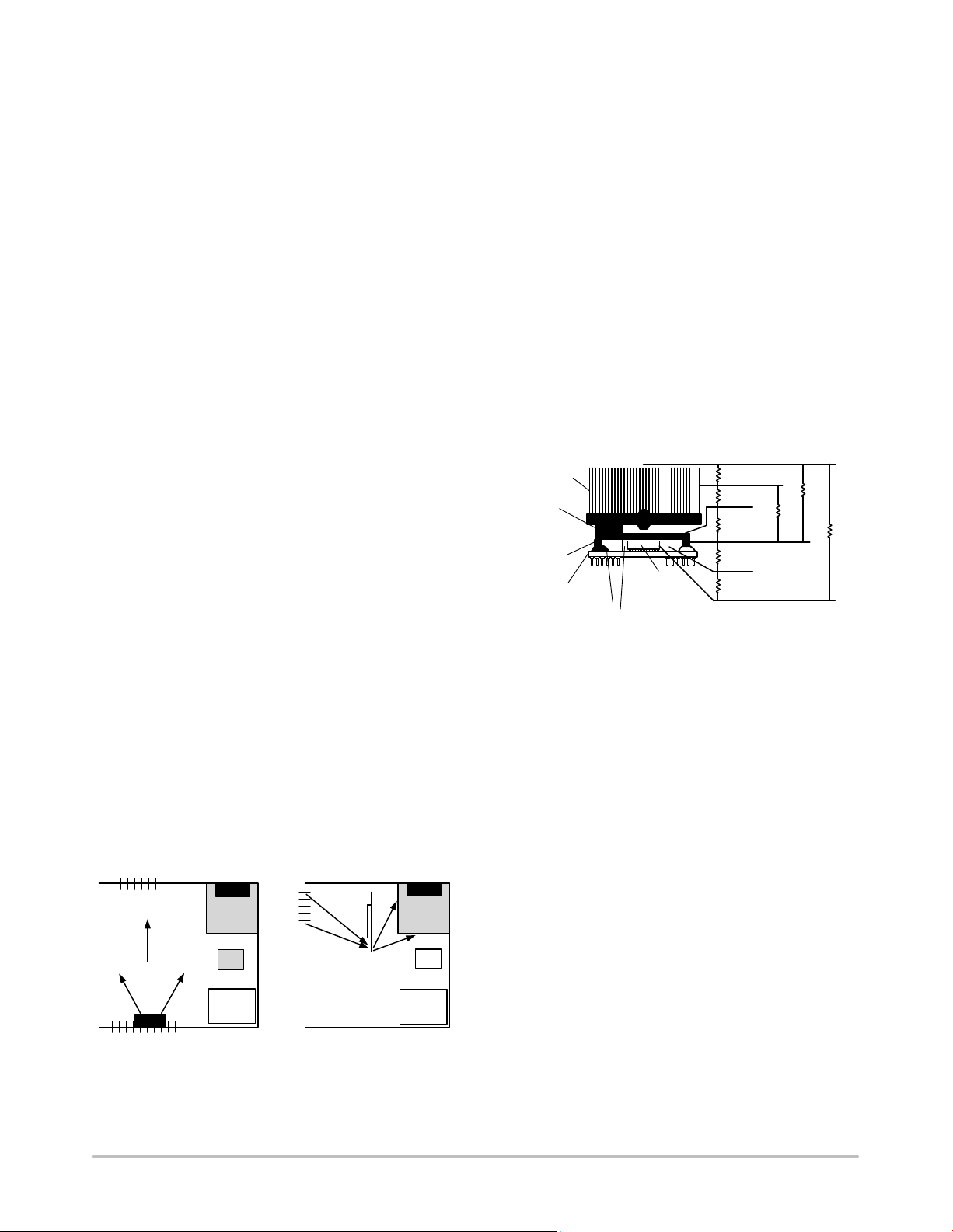
ADT7473
control allows the ADT7473/ADT7473−1 to intelligently
adapt the system’s cooling solution for best system
performance or lowest possible system acoustics, depending
on user or design requirements. Use of dynamic T
MIN
control alleviates the need to design for worst−case
conditions and significantly reduces system design and
validation time.
Designing for Worst−Case Conditions
System design must always allow for worst−case
conditions. In PC design, the worst−case conditions include,
but are not limited to, the following:
Worst−Case Altitude
A computer can be operated at different altitudes. The
altitude affects the relative air density, which alters the
effectiveness of the fan cooling solution. For example,
comparing 40°C air temperature at 10,000 feet to 20°C air
temperature at sea level, relative air density is increased by
40%. This means that the fan can spin 40% slower and make
less noise at sea level than at 10,000 feet while keeping the
system at the same temperature at both locations.
Worst−Case Fan
Due to manufacturing tolerances, fan speeds in RPM are
normally quoted with a tolerance of ±20%. The designer
needs to assume that the fan RPM can be 20% below
tolerance. This translates to reduced system airflow and
elevated system temperature. Note that fans 20% out of
tolerance can negatively impact system acoustics because
they run faster and generate more noise.
Worst−Case Chassis Airflow
The same motherboard can be used in a number of
different chassis configurations. The design of the chassis
and the physical location of fans and components determine
the system thermal characteristics. Moreover, for a given
chassis, the addition of add−in cards, cables, or other system
configuration options can alter the system airflow and
reduce the effectiveness of the system cooling solution. The
cooling solution can also be inadvertently altered by the end
user. (For example, placing a computer against a wall can
block the air ducts and reduce system airflow.)
VENTS
I/O CARDS
GOOD CPU AIRFLOW
FAN
VENTS
GOOD VENTING = GOOD AIR
EXCHANGE
POWER
SUPPLY
Figure 64. Chassis Airflow Issues
FAN
CPU
DRIVE
BAYS
VENTS
I/O CARDS
POOR CPU
AIRFLOW
POOR VENTING = POOR AIR
EXCHANGE
FAN
POWER
SUPPLY
CPU
DRIVE
BAYS
Worst−Case Processor Power Consumption
This data sheet maximum does not necessarily reflect the
true processor power consumption. Designing for
worst−case CPU power consumption can result in a
processor becoming overcooled (generating excess system
noise).
Worst−Case Peripheral Power Consumption
The tendency is to design to data sheet maximums for
peripheral components, again overcooling the system.
Worst−Case Assembly
Every system is unique because of manufacturing
variations. Heat sinks may be loose fitting or slightly
misaligned. Too much or too little thermal grease might be
used, or variations in application pressure for thermal
interface material could affect the efficiency of the thermal
solution. Accounting for manufacturing variations in every
system is difficult; therefore, the system must be designed
for the worst−case conditions.
T
A
HEAT
SINK
THERMAL
INTERFACE
MATERIAL
INTEGRATED
HEAT
SPREADER
SUBSTRATE
PROCESSOR
EPOXY
THERMAL INTERFACE MATERIAL
q
q
q
q
q
SA
TIMS
CTIM
TIMC
JTIM
T
S
q
T
TIM
T
C
T
TIM
T
J
CA
q
CS
q
JA
Figure 65. Thermal Model
Although a design usually accounts for worst−case
conditions in all these cases, the actual system is almost
never operated at worst−case conditions. The alternative to
designing for the worst case is to use the dynamic T
MIN
control function.
Dynamic T
Dynamic T
automatic fan control loop by adjusting the T
Control Overview
MIN
control mode builds on the basic
MIN
MIN
value
based on system performance and measured temperature.
This is important because, instead of designing for the worst
case, the system thermals can be defined as operating zones.
The ADT7473/ADT7473−1 can self−adjust its fan control
loop to maintain either an operating zone temperature or a
system target temperature. For example, it can be specified
that the ambient temperature in a system should be
maintained at 50°C. If the temperature is below 50°C, the
fans might not need to run, or might run very slowly. If the
temperature is higher than 50°C, the fans need to throttle up.
The challenge presented by any thermal design is finding
the right settings to suit the system’s fan control solution.
This can involve designing for the worst case, followed by
weeks of system thermal characterization, and finally fan
acoustic optimization (for psycho−acoustic reasons).
http://onsemi.com
43
Page 44
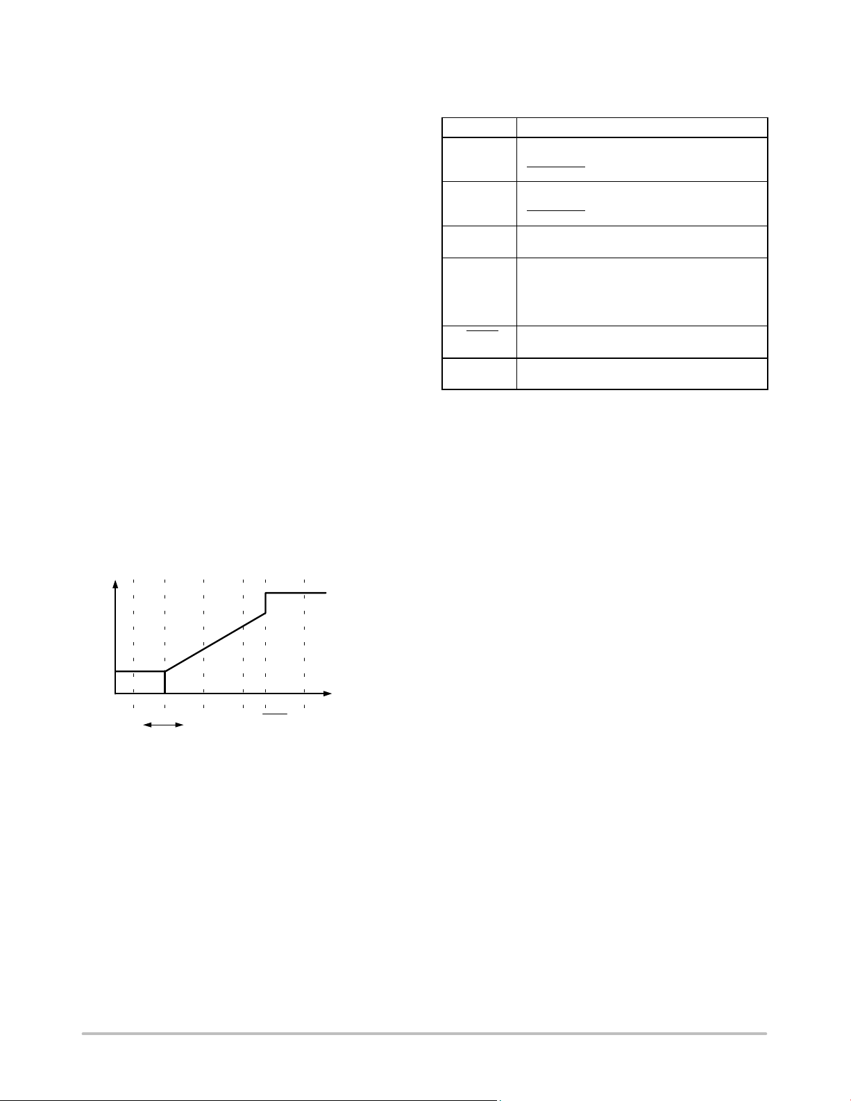
ADT7473
Getting the most benefit from the automatic fan control
mode involves characterizing the system to find the best
T
and T
MIN
PWM
value for the quietest fan speed setting. Using the
MIN
ADT7473/ADT7473−1’s dynamic T
settings for the control loop, and the best
RANGE
control mode,
MIN
however, shortens the characterization time and alleviates
tweaking the control loop settings because the device can
self−adjust during system operation.
Dynamic T
control mode is operated by specifying the
MIN
operating zone temperatures required for the system.
Associated with this control mode are three operating point
registers, one for each temperature channel. This allows the
system thermal solution to be broken down into distinct
thermal zones. For example, CPU operating temperature is
70°C, VRM operating temperature is 80°C, and ambient
operating temperature is 50°C. The ADT7473/ADT7473−1
dynamically alters the control solution to maintain each
zone temperature as closely as possible to its target operating
point.
Operating Point Registers
Register 0x33, Remote 1 Operating Point = 0xA4
(100°C default)
Register 0x34, Local Temperature Operating Point = 0xA4
(100°C default)
Register 0x35, Remote 2 Operating Point = 0xA4
(100°C default)
Figure 66 shows an overview of the parameters that affect
the operation of the dynamic T
PWM DUTY CYCLE
T
LOWTMIN
Figure 66. Dynamic T
OPERATING
POINT
T
HIGH
MIN
T
THERM
MIN
control loop.
TEMPERATURE
T
RANGE
Control Loop
Table 14 provides a brief description of each parameter.
Table 14. T
Parameter Description
T
LOW
T
HIGH
T
MIN
Operating
Point
T
THERM
T
RANGE
Dynamic T
Because the dynamic T
Control Loop Parameters
MIN
If the temperature drops below the T
an error flag is set in a status register and an
SMBALERT
If the temperature exceeds the T
error flag is set in a status register and an
SMBALERT interrupt can be generated.
The temperature at which the fan turns on
under automatic fan speed control.
The target temperature for a particular
temperature zone. The ADT7473/ADT7473−1
attempts to maintain system temperature at
about the operating point by adjusting the T
parameter of the control loop.
If the temperature exceeds this critical limit, the
fans can be run at 100% for maximum cooling.
Programs the PWM duty cycle vs. temperature
control slope.
Control Programming
MIN
interrupt can be generated.
HIGH
control mode is a basic
MIN
limit,
LOW
limit, an
MIN
extension of the automatic fan control mode, program the
automatic fan control mode parameters first, as described in
the Step 1: Hardware Configuration section to the Step 8:
T
for Temperature Channels section, then proceed with
HYST
dynamic T
control mode programming.
MIN
Step 9: Operating Points for Temperature Channels
The operating point for each temperature channel is the
optimal temperature for that thermal zone. The hotter each
zone is allowed to be, the quieter the system, because the
fans are not required to run as fast. The ADT7473/
ADT7473−1 increases or decreases fan speeds as necessary
to maintain the operating point temperature, allowing for
system−to−system variation and removing the need for
worst−case design. If a sensible operating point value is
chosen, any T
characterization. If the T
value can be selected in the system
MIN
value is too low, the fans run
MIN
sooner than required, and the temperature is below the
operating point. In response, the ADT7473/ADT7473−1
increases T
to keep the fans off longer and to allow the
MIN
temperature zone to get closer to the operating point.
Likewise, too high a T
value causes the operating point
MIN
to be exceeded, and in turn, the ADT7473/ADT7473−1
reduces T
to turn the fans on sooner to cool the system.
MIN
http://onsemi.com
44
Page 45
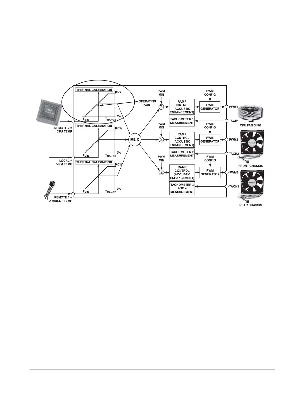
ADT7473
Programming Operating Point Registers
There are three operating point registers, one for each
temperature channel. These 8−bit registers allow the
operating point temperatures to be programmed with 1°C
resolution.
Operating Point Registers
Register 0x33, Remote 1 Operating Point = 0xA4
(100°C default)
Register 0x34, Local Operating Point = 0xA4
(100°C default)
Register 0x35, Remote 2 Operating Point = 0xA4
(100°C default).
Figure 67. Operating Point Value Dynamically Adjusts Automatic Fan Control Settings
Step 10: High and Low Limits for Temperature
Channels
The low limit defines the temperature at which the T
MIN
value starts to be increased, if temperature falls below this
value. This has the net effect of reducing the fan speed,
allowing the system to get hotter. An interrupt can be
generated when the temperature drops below the low limit.
The high limit defines the temperature at which the T
MIN
value starts to be reduced, if temperature increases above
this value. This has the net effect of increasing fan speed to
cool down the system. An interrupt can be generated when
the temperature rises above the high limit.
Programming High and Low Limits
There are six limit registers; a high limit and low limit are
associated with each temperature channel. These 8−bit
registers allow the high and low limit temperatures to be
programmed with 1°C resolution.
Temperature Limit Registers
Register 0x4E, Remote 1 Temperature Low Limit = 0x01
Register 0x4F, Remote 1 Temperature High Limit = 0x7F
Register 0x50, Local Temperature Low Limit = 0x01
Register 0x51, Local Temperature High Limit = 0x7F
Register 0x52, Remote 2 Temperature Low Limit = 0x01
Register 0x53, Remote 2 Temperature High Limit = 0x7F
How Dynamic T
Control Works
MIN
The basic premise is as follows:
1. Set the target temperature for the temperature
zone, which could be, for example, the Remote 1
thermal diode. This value is programmed to the
Remote 1 operating temperature register.
2. As the temperature in that zone (Remote 1
temperature) rises toward and exceeds the
operating point temperature, T
is reduced, and
MIN
the fan speed increases.
3. As the temperature drops below the operating
point temperature, T
is increased, and the fan
MIN
speed is reduced.
However, the loop operation is not as simple as described
in these steps. A number of conditions govern the situations
in which T
can increase or decrease.
MIN
http://onsemi.com
45
Page 46
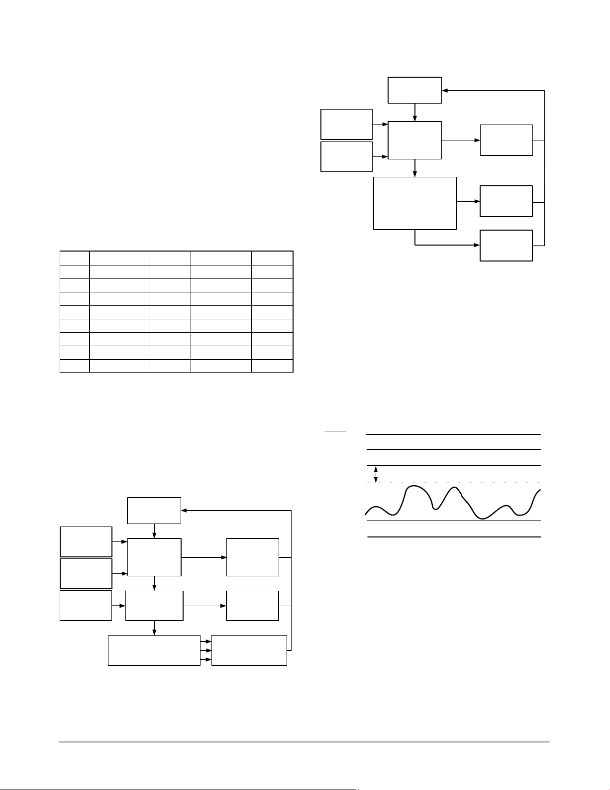
ADT7473
Short Cycle and Long Cycle
The ADT7473/ADT7473−1 implements two loops: a
short cycle and a long cycle. The short cycle takes place
every n monitoring cycles. The long cycle takes place every
2n monitoring cycles. The value of n is programmable for
each temperature channel. The bits are located at the
following register locations:
Remote 1 = CYR1 = Bits [2:0] of Dynamic T
MIN
Control
Register 2 (0x37).
Local = CYL = Bits [5:3] of Dynamic T
Control Register 2
MIN
(0x37).
Remote 2 = CYR2 = Bits [7:6] of Dynamic T
Register 2 (0x37) and Bit 0 of Dynamic T
MIN
MIN
Control
Control
Register 1 (0x36).
Table 15. Cycle Bit Assignments
Code Short Cycle Secs Long Cycle Secs
000 8 cycles 1 sec 16 cycles 2 sec
001 16 cycles 2 sec 32 cycles 4 sec
010 32 cycles 4 sec 64 cycles 8 sec
011 64 cycles 8 sec 128 cycles 16 sec
100 128 cycles 16 sec 256 cycles 32 sec
101 256 cycles 32 sec 512 cycles 64 sec
110 512 cycles 64 sec 1024 cycles 128 sec
111 1024 cycles 128 sec 2048 cycles 256 sec
Care should be taken when choosing the cycle time. A
long cycle time means that T
is updated less often. If
MIN
your system has very fast temperature transients, the
dynamic T
is chosen that is too fast, the full benefit of changing T
control loop is always lagging. If a cycle time
MIN
MIN
might not be realized and needs to change again on the next
cycle; in effect, it is overshooting. It is necessary to carry out
some calibration to identify the most suitable response time.
Figure 68 shows the steps taken during the short cycle.
Figure 69 shows the steps taken during the long cycle.
WAIT 2n
MONITORING
CYCLES
CURRENT
TEMPERATURE
MEASUREMENT
T1(n)
OPERATING
POINT
TEMPERATURE
OP1
IS T1(n) > OP1
IS T1(n) < LOW TEMP LIMIT
AND
T
< HIGH TEMP LIMIT
MIN
AND
< OP1
T
MIN
AND
T1(n) > T
NO
NO
MIN
YES
YES
DECREASE T
BY 15C
INCREASE
BY 15C
T
MIN
DO NOT
CHANGE
MIN
Figure 69. Long Cycle Steps
The following examples illustrate some of the
circumstances that might cause T
to increase, decrease,
MIN
or stay the same.
Example 1: Normal Operation—No T
Adjustment
MIN
• If measured temperature never exceeds the
programmed operating point minus the hysteresis
temperature, then T
is not adjusted; that is, it
MIN
remains at its current setting.
• If measured temperature never drops below the low
temperature limit, then T
THERM LIMIT
HIGH TEMP
LIMIT
OPERATING
POINT
HYSTERESIS
is not adjusted.
MIN
CURRENT
TEMPERATURE
MEASUREMENT
T1(n)
OPERATING
POINT
TEMPERATURE
OP1
PREVIOUS
TEMPERATURE
MEASUREMENT
T1 (n − 1)
WAIT n
MONITORING
CYCLES
IS T1(n) >
(OP1 − HYS)
IS T1(n) − T1(n − 1)
≤ 0.255C
IS T1(n) - T1(n - 1) = 0.5 - 0.755C
IS T1(n) - T1(n - 1) = 1.0 - 1.755C
IS T1(n) - T1(n - 1) > 2.05C
NO
YES
NO
DECREASE T
DECREASE T
DECREASE T
Figure 68. Short Cycle Steps
DO NOTHING
DO NOTHING
(SYSTEM IS
COOLING OFF
FOR CONSTANT)
BY 15C
MIN
BY 25C
MIN
BY 45C
MIN
http://onsemi.com
ACTUAL
TEMP
LOW TEMP
LIMIT
T
MIN
Figure 70. Temperature Between Operating Point
and Low Temperature Limit
Because neither the operating point minus the hysteresis
temperature nor the low temperature limit has been
exceeded, the T
a speed determined by the fixed T
value is not adjusted, and the fan runs at
MIN
and T
MIN
RANGE
defined in the automatic fan speed control mode.
Example 2: Operating Point Exceeded—T
Reduced
MIN
When the measured temperature is below the operating
point temperature minus the hysteresis, T
remains the
MIN
same.
Once the temperature exceeds the operating temperature
minus the hysteresis (OP − Hyst), T
starts to decrease.
MIN
This occurs during the short cycle (see Figure 68). The rate
46
values
Page 47
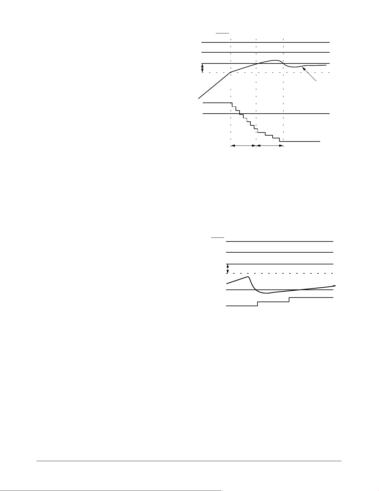
ADT7473
E
at which T
decreases depends on the programmed value
MIN
of n. It also depends on how much the temperature has
increased between this monitoring cycle and the last
monitoring cycle; that is, if the temperature has increased by
1°C, then T
is reduced by 2°C. Decreasing T
MIN
MIN
has the
effect of increasing the fan speed, thus providing more
cooling to the system.
If the temperature slowly increases only in the range
(OP − Hyst), that is, ≤0.25°C per short monitoring cycle,
then T
does not decrease. This allows small changes in
MIN
temperature in the desired operating zone without changing
T
. The long cycle makes no change to T
MIN
MIN
in the
temperature range (OP − Hyst) because the temperature has
not exceeded the operating temperature.
Once the temperature exceeds the operating temperature,
the long cycle causes T
to be reduced by 1°C every long
MIN
cycle while the temperature remains above the operating
temperature. This takes place in addition to the decrease in
T
that occurs due to the short cycle. In Figure 71, because
MIN
the temperature is increasing at a rate ≤0.25°C per short cycle,
no reduction in T
takes place during the short cycle.
MIN
Once the temperature falls below the operating
temperature, T
temperature starts to increase slowly, T
stays the same. Even when the
MIN
stays the same
MIN
because the temperature increases at a rate ≤0.25°C per cycle.
Example 3: Increase T
MIN
Cycle
When the temperature drops below the low temperature
limit, T
can increase in the long cycle. Increasing T
MIN
MIN
has the effect of running the fan slower and, therefore,
quieter. The long cycle diagram in Figure 69 shows the
conditions required for T
to increase. A quick summary
MIN
of those conditions and the reasons they need to be true
follows.
T
can increase if:
MIN
• The measured temperature falls below the low temperature
limit. This means the user must choose the low limit
carefully. It should not be so low that the temperature
never falls below it because T
and the fans would run faster than necessary.
• T
is below the high temperature limit. T
MIN
never allowed to increase above the high temperature
limit. As a result, the high limit should be sensibly
chosen because it determines how high T
• T
is below the operating point temperature. T
MIN
should never be allowed to increase above the operating
point temperature because the fans would not switch on
until the temperature rose above the operating point.
• The temperature is above T
control is turned off below T
would never increase,
MIN
MIN
. The dynamic T
MIN
.
MIN
is
MIN
can go.
MIN
MIN
THERM
LIMIT
HIGH TEMP
LIMIT
OPERATING
POINT
HYSTERESIS
ACTUAL
TEMP
T
MIN
LOW TEMP
LIMIT
DECREASE HERE DUE TO
SHORT CYCLE ONLY
T1(n) - T1 (n - 1) = 0.55C
OR 0.755C = > T
DECREASES BY 15C
EVERY SHORT CYCLE
MIN
DECREASE HERE DUE TO
LONG CYCLE ONLY
T1(n) - T1 (n - 1) ≤ 0.255C
AND T1(n) > OP = > TMIN
DECREASES BY 15C
EVERY LONG CYCLE
NO CHANGE IN T
DUE TO ANY CYCLE BECAUS
T1(n) - T1 (n - 1) ≤ 0.255C
AND T1(n) < OP = > TMIN
STAYS THE SAME
MIN
HERE
Figure 71. Effect of Exceeding Operating Point Minus
Hysteresis Temperature
Figure 72 shows how T
temperature is above T
limit, and T
is below the high temperature limit and
MIN
increases when the current
MIN
and below the low temperature
MIN
below the operating point. Once the temperature rises above
the low temperature limit, T
THERM
LIMIT
HIGH TEMP
LIMIT
OPERATING
POINT
HYSTERESIS
ACTUAL
LOW TEMP
LIMIT
T
MIN
TEMP
Figure 72. Increasing T
Example 4: Preventing T
Because T
for T
MIN
to reach full scale (127°C) because the fan would
is dynamically adjusted, it is undesirable
MIN
never switch on. As a result, T
stays the same.
MIN
for Quieter Operation
MIN
from Reaching Full Scale
MIN
is allowed to vary only
MIN
within a specified range:
• The lowest possible value for T
is −127°C (twos
MIN
complement mode) or −64°C (Offset 64 mode).
• T
• If the temperature is below T
cannot exceed the high temperature limit.
MIN
, the fan is switched
MIN
off or runs at minimum speed and dynamic T
MIN
control is disabled.
http://onsemi.com
47
Page 48

ADT7473
THERM
LIMIT
OPERATING
POINT
LOW TEMP
HIGH TEMP
Figure 73. T
Step 11: Monitoring THERM
LIMIT
LIMIT
T
MIN
HYSTERESIS
ACTUAL
TEMP
T
PREVENTED
MIN
FROM INCREASING
Adjustments Limited by the High
MIN
Temperature Limit
Using the operating point limit ensures that the dynamic
T
control mode operates in the best possible acoustic
MIN
position while ensuring that the temperature never exceeds
the maximum operating temperature. Using the operating
point limit allows T
to be independent of system−level
MIN
issues because of its self−corrective nature. In PC design, the
operating point for the chassis is usually the worst−case
internal chassis temperature.
The optimal operating point for the processor is
determined by monitoring the thermal monitor in the Intel
Pentium 4 processor. To do this, the PROCHOT
the Pentium 4 is connected to the THERM
output of
input of the
ADT7473/ADT7473−1.
The operating point for the processor can be determined
by allowing the current temperature to be copied to the
operating point register when the PROCHOT
the THERM
input low on the ADT7473/ADT7473−1. This
output pulls
gives the maximum temperature at which the Pentium 4 can
run before clock modulation occurs.
Enabling the THERM Trip Point as the Operating Point
Bits [4:2] of Dynamic T
enable/disable THERM
Control Register 1 (0x36)
MIN
monitoring to program the
operating point.
Dynamic T
Control Register 1 (0x36)
MIN
Bit [4] PHTR2 = 1, copies the Remote 2 current temperature
to the Remote 2 operating point register, if THERM
is
asserted. The operating point contains the temperature at
which THERM
is asserted. This allows the system to run as
quietly as possible without affecting system performance.
PHTR2 = 0, ignores any THERM
assertions. The Remote 2
operating point register reflects its programmed value.
Bit [3] PHTL = 1, copies the local current temperature to the
local temperature operating point register if THERM
is
asserted. The operating point contains the temperature at
which THERM
is asserted. This allows the system to run as
quietly as possible without affecting system performance.
PHTL = 0, ignores any THERM
assertions. The local
temperature operating point register reflects its programmed
value.
Bit [2] PHTR1 = 1, copies the Remote 1 current temperature
to the Remote 1 operating point register if THERM
is
asserted. The operating point contains the temperature at
which THERM
is asserted. This allows the system to run as
quietly as possible without affecting system performance.
PHTR1 = 0, ignores any THERM
assertions. The Remote 1
operating point register reflects its programmed value.
Enabling Dynamic T
Bits [7:5] of the Dynamic T
enable/disable dynamic T
Control Mode
MIN
MIN
control on the temperature
MIN
Control Register 1 (0x36)
channels.
Dynamic
Bit [7] R2T = 1, enables dynamic T
Remote 2 temperature channel. The chosen T
Control Register 1 (0x36)
TMIN
control on the
MIN
MIN
value is
dynamically adjusted based on the current temperature,
operating point, and high and low limits for this zone.
R2T = 0, disables dynamic T
control. The T
MIN
MIN
value
chosen is not adjusted and the channel behaves as described
in the Automatic Fan Control Overview section.
Bit [6] LT = 1, enables dynamic T
temperature channel. The chosen T
control on the local
MIN
value is dynamically
MIN
adjusted based on the current temperature, operating point,
and high and low limits for this zone.
LT = 0, disables dynamic T
control. The T
MIN
MIN
value
chosen is not adjusted and the channel behaves as described
in the Automatic Fan Control Overview section.
Bit [5] R1T = 1, enables dynamic T
Remote 1 temperature channel. The chosen T
control on the
MIN
MIN
value is
dynamically adjusted based on the current temperature,
operating point, and high and low limits for this zone.
R1T = 0, disables dynamic T
control. The T
MIN
MIN
value
chosen is not adjusted, and the channel behaves as described
in the Automatic Fan Control Overview section.
Enhancing System Acoustics
Automatic fan speed control mode reacts instantaneously
to changes in temperature; that is, the PWM duty cycle
responds immediately to temperature change. Any impulses
in temperature can cause an impulse in fan noise. For
psycho−acoustic reasons, the ADT7473/ADT7473−1 can
prevent the PWM output from reacting instantaneously to
temperature changes. Enhanced acoustic mode controls the
maximum change in PWM duty cycle at a given time. The
objective is to prevent the fan from cycling up and down,
annoying the user.
Acoustic Enhancement Mode Overview
Figure 74 gives a top−level overview of the automatic fan
control circuitry on the ADT7473/ADT7473−1 and shows
where acoustic enhancement fits in. Acoustic enhancement
is intended as a post design tweak made by a system or
mechanical engineer evaluating best settings for the system.
Having determined the optimal settings for the thermal
http://onsemi.com
48
Page 49
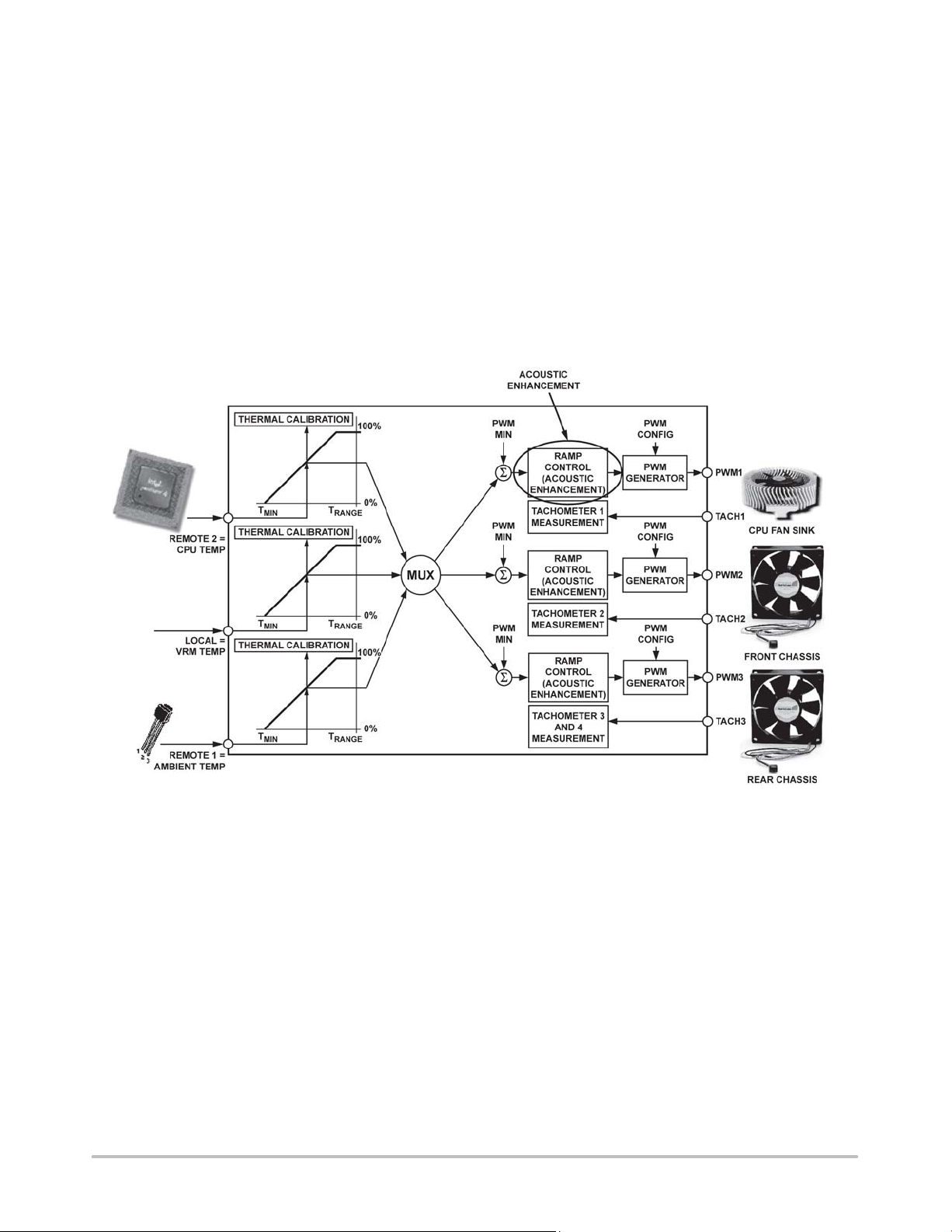
ADT7473
solution, the engineer can adjust the system acoustics. The
goal is to implement a system that is acoustically pleasing
without causing user annoyance due to fan cycling. It is
important to realize that although a system might pass an
acoustic noise requirement specification (for example,
36 dB), if the fan is annoying, it fails the consumer test.
Approaches to System Acoustic Enhancement
There are two different approaches to implementing
system acoustic enhancement: temperature−centric and
fan−centric.
The temperature−centric approach involves smoothing
transient temperatures as they are measured by a
temperature source (for example, Remote 1 temperature).
The temperature values used to calculate the PWM duty
cycle values are smoothed, reducing fan speed variation.
However, this approach causes an inherent delay in updating
fan speed and causes the thermal characteristics of the
system to change. It also causes the system fans to stay on
longer than necessary because the fan’s reaction is merely
delayed. The user has no control over noise from different
fans driven by the same temperature source. Consider, for
example, a system in which control of a CPU cooler fan (on
PWM1) and a chassis fan (on PWM2) use Remote 1
temperature. Because the Remote 1 temperature is
smoothed, both fans are updated at exactly the same rate. If
the chassis fan is much louder than the CPU fan, there is no
way to improve its acoustics without changing the thermal
solution of the CPU cooling fan.
Figure 74. Acoustic Enhancement Smoothes Fan Speed Variations Under Automatic Fan Speed Control
The fan−centric approach to system acoustic
enhancement controls the PWM duty cycle, driving the fan
at a fixed rate (for example, 6%). Each time the PWM duty
cycle is updated, it is incremented by a fixed 6%. As a result,
the fan ramps smoothly to its newly calculated speed. If the
temperature starts to drop, the PWM duty cycle immediately
placed into acoustic enhancement mode independently of
PWM1. The acoustics of the chassis fan can, therefore, be
adjusted without affecting the acoustic behavior of the CPU
cooling fan, even though both fans are controlled by Remote
1 temperature. The fan−centric approach is how acoustic
enhancement works on the ADT7473/ADT7473−1.
decreases by 6% at every update. Therefore, the fan ramps
smoothly up or down without inherent system delay.
Consider, for example, controlling the same CPU cooler fan
(on PWM1) and chassis fan (on PWM2) using Remote 1
temperature. The T
MIN
and T
settings have already
RANGE
been defined in automatic fan speed control mode, that is,
thermal characterization of the control loop has been
optimized. Here, the chassis fan is noisier than the CPU
cooling fan. Using the fan−centric approach, PWM2 can be
http://onsemi.com
Enabling Acoustic Enhancement for Each PWM
Output
Enhanced acoustics Register 1 (0x62)
Bit 3 = 1, enables acoustic enhancement on PWM1 output
Enhanced acoustics Register 2 (0x63)
Bit 7 = 1, enables acoustic enhancement on PWM2 output
Bit 3 = 1, enables acoustic enhancement on PWM3 output
49
Page 50
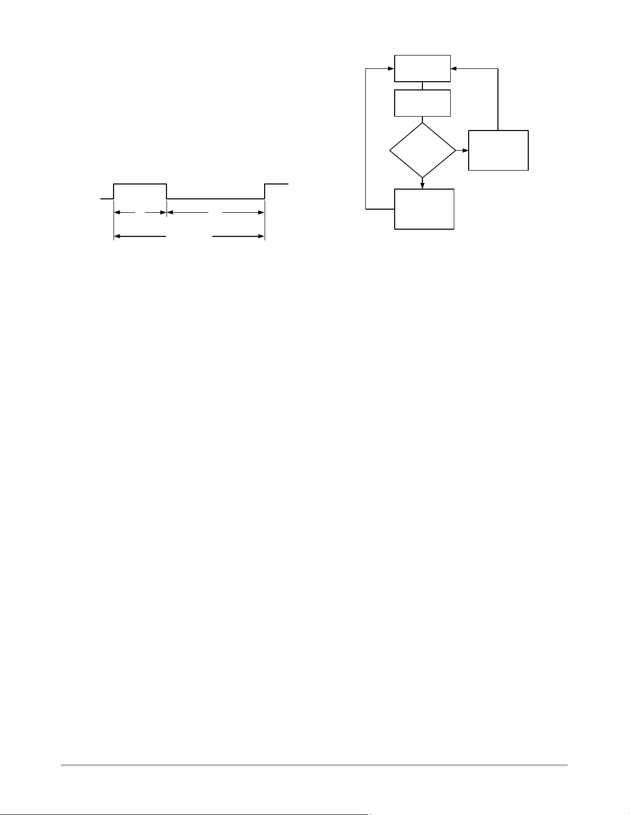
ADT7473
Effect of Ramp Rate on Enhanced Acoustics Mode
The PWM signal driving the fan has a period, T, given by
the PWM drive frequency, f, because T = 1/f. For a given
PWM period, T, the PWM period is subdivided into 255
equal time slots. One time slot corresponds to the smallest
possible increment in the PWM duty cycle. A PWM signal
of 33% duty cycle is, therefore, high for 1/3 x 255 time slots
and low for 2/3 x 255 time slots. Therefore, a 33% PWM
duty cycle corresponds to a signal that is high for 85 time
slots and low for 170 time slots.
PWM_OUT
33% DUTY
CYCLE
85
TIME SLOTS
PWM OUTPUT
(ONE PERIOD)
= 255 TIME SLOTS
Figure 75. 33% PWM Duty Cycle Represented
in Time Slots
170
TIME SLOTS
The ramp rates in the enhanced acoustics mode are
selectable from the values 1, 2, 3, 5, 8, 12, 24, and 48. The
ramp rates are discrete time slots. For example, if the ramp
rate is 8, then eight time slots are added to the PWM high duty
cycle each time the PWM duty cycle needs to be increased.
If the PWM duty cycle value needs to be decreased, it is
decreased by eight time slots. Figure 76 shows how the
enhanced acoustics mode algorithm operates.
The enhanced acoustics mode algorithm calculates a new
PWM duty cycle based on the temperature measured. If the
new PWM duty cycle value is greater than the previous
PWM value, then the previous PWM duty cycle value is
incremented by either 1, 2, 3, 5, 8, 12, 24, or 48 time slots,
depending on the settings of the enhanced acoustics
registers. If the new PWM duty cycle value is less than the
previous PWM value, the previous PWM duty cycle is
decremented by 1, 2, 3, 5, 8, 12, 24, or 48 time slots. Each
time the PWM duty cycle is incremented or decremented, its
value is stored as the previous PWM duty cycle for the next
comparison. A ramp rate of 1 corresponds to one time slot,
which is 1/255 of the PWM period. In enhanced acoustics
mode, incrementing or decrementing by 1 changes the PWM
output by 1/255 x 100%.
READ
TEMPERATURE
CALCULATE
NEW PWM
DUTY CYCLE
IS NEW PWM
VALUE >
PREVIOUS
VALUE?
YES
INCREMENT
PREVIOUS
PWM VALUE
BY RAMP RATE
DECREMENT
NO
PWM VALUE
BY RAMP RATE
PREVIOUS
Figure 76. Enhanced Acoustics Algorithm
Step 12: Ramp Rate for Acoustic Enhancement
The optimal ramp rate for acoustic enhancement can be
found through system characterization after the thermal
optimization has been finished. The effect of each ramp rate
should be logged, if possible, to determine the best setting
for a given solution.
Enhanced Acoustics Register 1 (0x62)
Bits [2:0] ACOU, select the ramp rate for PWM1.
000 = 1 time slot = 35 sec
001 = 2 time slots = 17.6 sec
010 = 3 time slots = 11.8 sec
011 = 5 time slots = 7 sec
100 = 8 time slots = 4.4 sec
101 = 12 time slots = 3 sec
110 = 24 time slots = 1.6 sec
111 = 48 time slots = 0.8 sec
Enhanced Acoustics Register 2 (0x63)
Bits [2:0] ACOU3, select the ramp rate for PWM3.
000 = 1 time slot = 35 sec
001 = 2 time slots = 17.6 sec
010 = 3 time slots = 11.8 sec
011 = 5 time slots = 7 sec
100 = 8 time slots = 4.4 sec
101 = 12 time slots = 3 sec
110 = 24 time slots = 1.6 sec
111 = 48 time slots = 0.8 sec
Bits [6:4] ACOU2, select the ramp rate for PWM2.
000 = 1 time slot = 35 sec
001 = 2 time slots = 17.6 sec
010 = 3 time slots = 11.8 sec
011 = 5 time slots = 7 sec
100 = 8 time slots = 4.4 sec
101 = 12 time slots = 3 sec
110 = 24 time slots = 1.6 sec
111 = 48 time slots = 0.8 sec
http://onsemi.com
50
Page 51
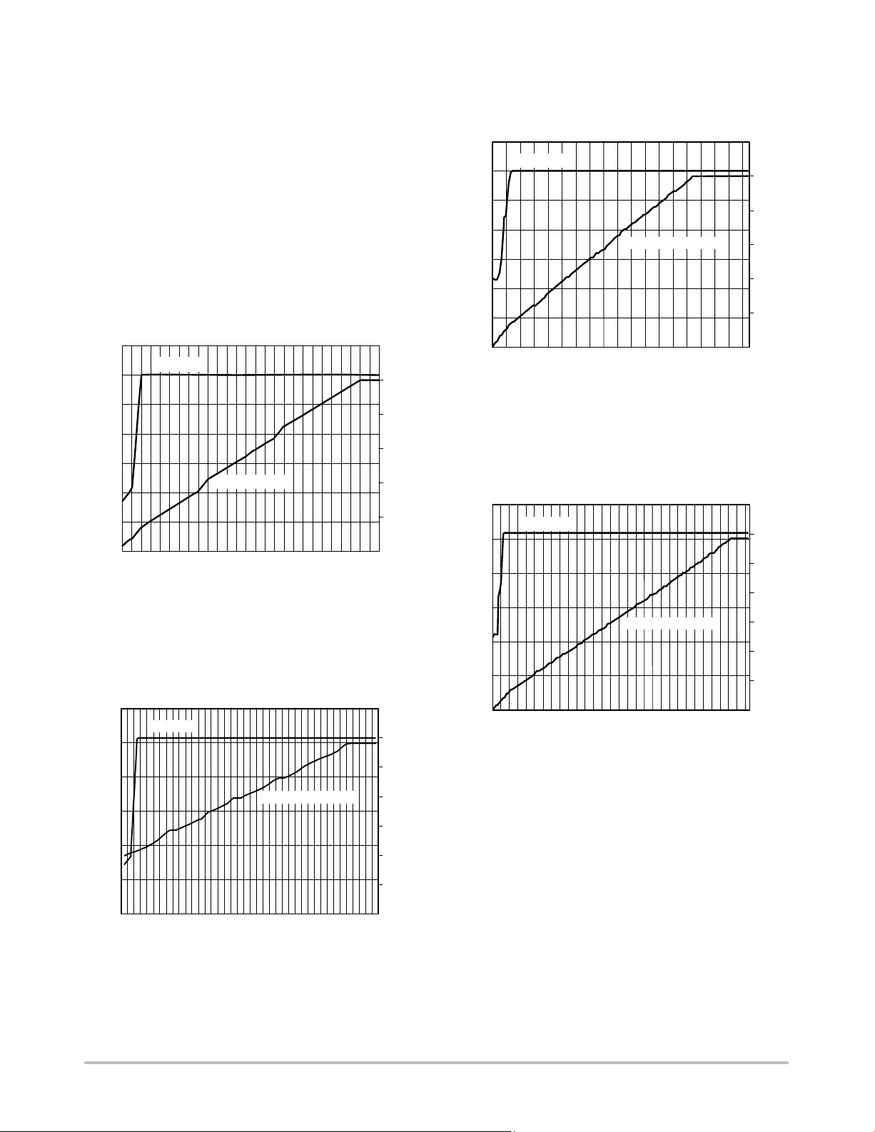
ADT7473
Another way to view the ramp rates is to measure the time
it takes for the PWM output to ramp up from 0% to 100%
duty cycle for an instantaneous change in temperature. This
can be tested by putting the ADT7473/ADT7473−1 into
manual mode and changing the PWM output from 0% to
100% PWM duty cycle. The PWM output takes 35 seconds
to reach 100% when a ramp rate of 1 time slot is selected.
Figure 77 shows remote temperature plotted against
PWM duty cycle for enhanced acoustics mode. The ramp
rate is set to 48, which corresponds to the fastest ramp rate.
Assume that a new temperature reading is available every
115 ms. With these settings, it takes approximately 0.76
seconds to go from 33% duty cycle to 100% duty cycle (full
speed). Even though the temperature increases very rapidly,
the fan ramps up to full speed gradually.
140
R
(5C)
120
100
(5C)
TEMP
R
80
60
40
20
0
TEMP
PWM CYCLE (%)
0 0.76
TIME (s)
Figure 77. Enhanced Acoustics Mode with
Ramp Rate = 48
120
100
80
60
40
20
0
Figure 78 shows how changing the ramp rate from 48 to
8 affects the control loop. The overall response of the fan is
slower. Because the ramp rate is reduced, it takes longer for
the fan to achieve full running speed. In this case, it takes
approximately 4.4 seconds for the fan to reach full speed.
120
100
(5C)
TEMP
R
R
(5C)
TEMP
80
60
40
20
PWM DUTY CYCLE (%)
140
120
100
80
60
40
20
Figure 79 shows the PWM output response for a ramp rate
of 2. In this instance, the fan takes about 17.6 seconds to
reach full running speed.
140
120
100
80
(5C)
TEMP
60
R
40
20
0
0
Figure 80 shows how the control loop reacts to
temperature with the slowest ramp rate. The ramp rate is set
to 1, while all other control parameters remain the same.
With the slowest ramp rate selected, it takes 35 seconds for
PWM CYCLE (%)
the fan to reach full speed.
120
100
80
(5C)
60
TEMP
R
40
20
0
0
As Figure 77 to Figure 80 show, the rate at which the fan
reacts to temperature change is dependent on the ramp rate
selected in the enhanced acoustics registers. The higher the
ramp rate, the faster the fan reaches the newly calculated fan
PWM DUTY CYCLE (%)
speed.
(5C)
R
TEMP
PWM DUTY CYCLE (%)
TIME (s)
17.6
Figure 79. Enhanced Acoustics Mode with
Ramp Rate = 2
(5C)
R
TEMP
PWM DUTY CYCLE (%)
TIME (s)
35
Figure 80. Enhanced Acoustics Mode with
Ramp Rate = 1
120
100
80
60
40
PWM DUTY CYCLE (%)
20
0
140
120
100
80
60
40
PWM DUTY CYCLE (%)
20
0
0
0
TIME (s)
4.4
Figure 78. Enhanced Acoustics Mode with
Ramp Rate = 8
0
http://onsemi.com
51
Page 52
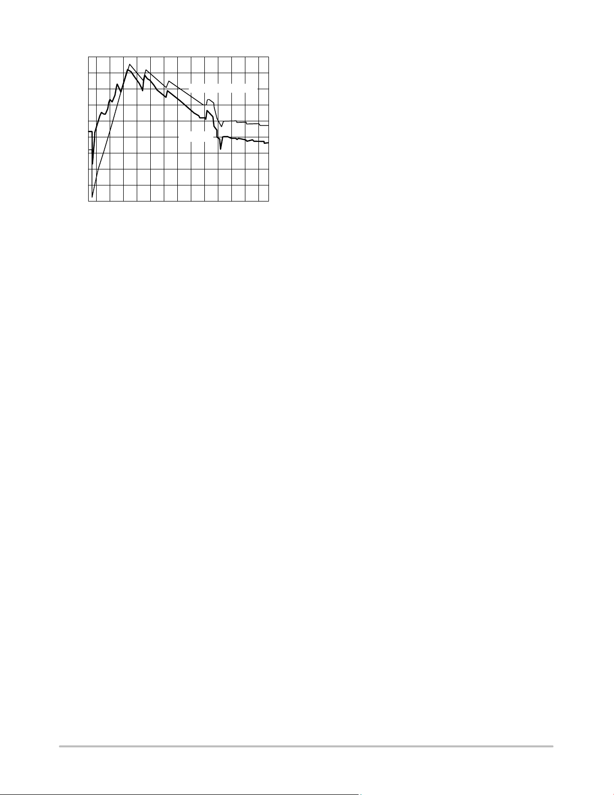
ADT7473
(5C)
TEMP
R
90
80
70
60
50
40
30
20
10
0
PWM DUTY CYCLE (%)
R
TEMP
TIME (s)
(5C)
90
80
70
60
50
40
30
20
10
0
Figure 81. How Fan Reacts to Temperature Variation
in Enhanced Acoustics Mode
Figure 81 shows the behavior of the PWM output as
temperature varies. As the temperature increases, the fan
speed ramps up. Small drops in temperature do not affect the
ramp−up function because the newly calculated fan speed is
still higher than the previous PWM value. Enhanced
acoustics mode allows the PWM output to be made less
sensitive to temperature variations. This is dependent on the
ramp rate selected and programmed into the enhanced
acoustics registers.
Slower Ramp Rates
The ADT7473/ADT7473−1 can be programmed for
much longer ramp times by slowing the ramp rates. Each
ramp rate can be slowed by a factor of 4.
PWM1 Configuration Register (0x5C)
Bit [3] SLOW, 1 slows the ramp rate for PWM1 by 4.
PWM2 Configuration Register (0x5D)
Bit [3] SLOW, 1 slows the ramp rate for PWM2 by 4.
PWM3 Configuration Register (0x5E)
Bit [3] SLOW, 1 slows the ramp rate for PWM3 by 4.
The following sections list the ramp−up times when the
SLOW bit is set for each PWM output.
Enhanced Acoustics Register 1 (0x62)
Bits [2:0] ACOU, select the ramp rate for PWM1.
000 = 140 sec
PWM DUTY CYCLE (%)
001 = 70.4 sec
010 = 47.2 sec
011 = 28 sec
100 = 17.6 sec
101 = 12 sec
110 = 6.4 sec
111 = 3.2 sec
Enhanced Acoustics Register 2 (0x63)
Bits [2:0] ACOU3, select the ramp rate for PWM3.
000 = 140 sec
001 = 70.4 sec
010 = 47.2 sec
011 = 28 sec
100 = 17.6 sec
101 = 12 sec
110 = 6.4 sec
111 = 3.2 sec
Bits [6:4] ACOU2, select the ramp rate for PWM2.
000 = 140 sec
001 = 70.4 sec
010 = 47.2 sec
011 = 28 sec
100 = 17.6 sec
101 = 12 sec
110 = 6.4 sec
111 = 3.2 sec
http://onsemi.com
52
Page 53

ADT7473
Register Tables
Table 16. ADT7473/ADT7473−1 Registers
Addr R/W Desc Bit 7 Bit 6 Bit 5 Bit 4 Bit 3 Bit 2 Bit 1 Bit 0 De-
0x21 R V
0x22 R V
0x25 R Remote 1
0x26 R Local
0x27 R Remote 2
0x28 R TACH1 Low
0x29 R TACH1
0x2A R TACH2 Low
0x2B R TACH2
0x2C R TACH3 Low
0x2D R TACH3
0x2E R TACH4 Low
0x2F R TACH4
0x30 R/W PWM1
0x31 R/W PWM2
0x32 R/W PWM3
0x33 R/W Remote 1
0x34 R/W Local Temp
0x35 R/W Remote 2
0x36 R/W Dynamic
0x37 R/W Dynamic
0x38 R/W PWM1 Max
0x39 R/W PWM2 Max
0x3A R/W PWM3 Max
CCP
Reading
CC
Reading
Te m p.
Te mp .
Te m p.
Byte
High Byte
Byte
High Byte
Byte
High Byte
Byte
High Byte
Current
Duty Cycle
Current
Duty Cycle
Current
Duty Cycle
Operating
Point
Operating
Point
Operating
Point
T
MIN
Control
Reg. 1
T
MIN
Control
Reg. 2
Duty Cycle
Duty Cycle
Duty Cycle
9 8 7 6 5 4 3 2 0x00 −
9 8 7 6 5 4 3 2 0x00 −
9 8 7 6 5 4 3 2 0x01 −
9 8 7 6 5 4 3 2 0x01 −
9 8 7 6 5 4 3 2 0x01 −
7 6 5 4 3 2 1 0 0x00 −
15 14 13 12 11 10 9 8 0x00 −
7 6 5 4 3 2 1 0 0x00 −
15 14 13 12 11 10 9 8 0x00 −
7 6 5 4 3 2 1 0 0x00 −
15 14 13 12 11 10 9 8 0x00 −
7 6 5 4 3 2 1 0 0x00 −
15 14 13 12 11 10 9 8 0x00 −
7 6 5 4 3 2 1 0 0x00/0
7 6 5 4 3 2 1 0 0x00/0
7 6 5 4 3 2 1 0 0x00/0
7 6 5 4 3 2 1 0 0xA4 Ye s
7 6 5 4 3 2 1 0 0xA4 Ye s
7 6 5 4 3 2 1 0 0xA4 Ye s
R2T LT R1T PHTR2 PHTL PHTR1 V
CYR2 CYR2 CYL CYL CYL CYR1 CYR1 CYR1 0x00 Ye s
7 6 5 4 3 2 1 0 0xFF −
7 6 5 4 3 2 1 0 0xFF −
7 6 5 4 3 2 1 0 0xFF −
LO CYR2 0x00 Ye s
CCP
fault
xFF
xFF
xFF
Lock-
able
−
−
−
http://onsemi.com
53
Page 54

ADT7473
Table 16. ADT7473/ADT7473−1 Registers
Addr Lock-
0x3D R Device ID
0x3E R Company
0x3F R Revision ID
0x40 R/W Config.
0x41 R Interrupt
0x42 R Interrupt
0x46 R/W V
0x47 R/W V
0x48 R/W VCC Low
0x49 R/W VCC High
0x4E R/W Remote 1
0x4F R/W Remote 1
0x50 R/W Local Temp.
0x51 R/W Local Temp.
0x52 R/W Remote 2
0x53 R/W Remote 2
0x54 R/W TACH1
0x55 R/W TACH1
0x56 R/W TACH2
0x57 R/W TACH2
0x58 R/W TACH3
0x59 R/W TACH3
Register
ID Number
Register
Register 1
Status
Register 1
Status
Register 2
Low
CCP
Limit
High
CCP
Limit
Limit
Limit
Temp . L ow
Limit
Temp . H ig h
Limit
Low Limit
High Limit
Temp . L ow
Limit
Temp . H ig h
Limit
Minimum
Low Byte
Minimum
High Byte
Minimum
Low Byte
Minimum
High Byte
Minimum
Low Byte
Minimum
High Byte
7 6 5 4 3 2 1 0 0x73 −
7 6 5 4 3 2 1 0 0x41 −
7 6 5 4 3 2 1 0 0x68/0
ADT7473:
RES
ADT7473−1:
Latch Reset
OOL R2T LT R1T RES V
D2 D1 F4P FAN 3 FAN2 FA N1 OVT ADT7473:
7 6 5 4 3 2 1 0 0x00 −
7 6 5 4 3 2 1 0 0xFF −
7 6 5 4 3 2 1 0 0x00 −
7 6 5 4 3 2 1 0 0xFF −
7 6 5 4 3 2 1 0 0x01 −
7 6 5 4 3 2 1 0 0xFF −
7 6 5 4 3 2 1 0 0x01 −
7 6 5 4 3 2 1 0 0xFF −
7 6 5 4 3 2 1 0 0x01 −
7 6 5 4 3 2 1 0 0xFF −
7 6 5 4 3 2 1 0 0xFF −
15 14 13 12 11 10 9 8 0xFF −
7 6 5 4 3 2 1 0 0xFF −
15 14 13 12 11 10 9 8 0xFF −
7 6 5 4 3 2 1 0 0xFF −
15 14 13 12 11 10 9 8 0xFF −
TODIS FSPDIS Vx1 FSPD RDY LOCK STRT 0x01 Yes
V
CC
CCP
Bit 0Bit 1Bit 2Bit 3Bit 4Bit 5Bit 6Bit 7DescR/W
RES 0x00 −
RES
ADT7473−1:
THERM
Limit Latch
De-
fault
x69
0x00 −
able
−
http://onsemi.com
54
Page 55

ADT7473
Table 16. ADT7473/ADT7473−1 Registers
Addr Lock-
0x5A R/W TACH4
0x5B R/W TACH4
0x5C R/W PWM1
0x5D R/W PWM2
0x5E R/W PWM3
0x5F R/W Remote 1
0x60 R/W Local
0x61 R/W Remote 2
0x62 R/W Enhanced
0x63 R/W Enhanced
0x64 R/W PWM1 Min
0x65 R/W PWM2 Min
0x66 R/W PWM3 Min
0x67 R/W Remote 1
0x68 R/W Local Temp.
0x69 R/W Remote 2
0x6A R/W Remote 1
0x6B R/W Local
0x6C R/W Remote 2
0x6D R/W Remote 1
0x6E R/W Remote 2
0x6F R/W XNOR Tree
Minimum
Low Byte
Minimum
High Byte
Config.
Register
Config.
Register
Config.
Register
T
RANGE
PWM 1
Frequency
T
RANGE
PWM 2
Frequency
T
RANGE
PWM 3
Frequency
Acoustics
Reg. 1
Acoustics
Reg. 2
Duty Cycle
Duty Cycle
Duty Cycle
Temp . T
MIN
T
MIN
Temp . T
MIN
THERM
Temp. Limit
THERM
Temp. Limit
THERM
Temp. Limit
and Local
Te m p/ T
MIN
Hysteresis
Te m p/ T
MIN
Hysteresis
Test Enable
/
/
/
7 6 5 4 3 2 1 0 0xFF −
15 14 13 12 11 10 9 8 0xFF −
BHVR BHVR BHVR INV SLOW SPIN SPIN SPIN 0x82/0
BHVR BHVR BHVR INV SLOW SPIN SPIN SPIN 0x82/0
BHVR BHVR BHVR INV SLOW SPIN SPIN SPIN 0x82/0
RANGE RANGE RANGE RANGE HF/LF
RANGE RANGE RANGE RANGE HF/LF
RANGE RANGE RANGE RANGE HF/LF
MIN3 MIN2 MIN1 SYNC EN1 ACOU ACOU ACOU 0x00 Yes
EN2 ACOU2 ACOU2 ACOU2 EN3 ACOU3 ACOU3 ACOU3 0x00 Yes
7 6 5 4 3 2 1 0 0x80 Ye s
7 6 5 4 3 2 1 0 0x80 Ye s
7 6 5 4 3 2 1 0 0x80 Ye s
7 6 5 4 3 2 1 0 0x9A Ye s
7 6 5 4 3 2 1 0 0x9A Ye s
7 6 5 4 3 2 1 0 0x9A Ye s
7 6 5 4 3 2 1 0 0xA4 Ye s
7 6 5 4 3 2 1 0 0xA4 Ye s
7 6 5 4 3 2 1 0 0xA4/0
HYSR1 HYSR1 HYSR1 HYSR1 HYSL HYSL HYSL HYSL 0x44 Yes
HYSR2 HYSR2 HYSR2 HYRS2 RES RES RES RES 0x40 Ye s
RES RES RES RES RES RES RES XEN 0x00 Ye s
Fan 1
Fan 2
Fan 3
FREQ FREQ FREQ 0xCC Yes
FREQ FREQ FREQ 0xCC Yes
FREQ FREQ FREQ 0xCC Yes
Bit 0Bit 1Bit 2Bit 3Bit 4Bit 5Bit 6Bit 7DescR/W
De-
fault
x62
x62
x62
xC8
able
Yes
Yes
Yes
Yes
http://onsemi.com
55
Page 56

ADT7473
Table 16. ADT7473/ADT7473−1 Registers
Addr Lock-
0x70 R/W Remote 1
0x71 R/W Local Temp.
0x72 R/W Remote 2
0x73 R/W Config.
0x74 R/W Interrupt
0x75 R/W Interrupt
0x76 R Extended
0x77 R Extended
0x78 R/W Config.
0x79 R THERM
0x7A R/W THERM
0x7B R/W TA CH
0x7C R/W Config.
0x7D R/W Config.
0x7E R Te s t
0x7F R Te s t
0x80 R Te s t
Te m p.
Offset
Offset
Te m p.
Offset
Register 2
Mask
Register 1
Mask
Register 2
Resolution
1
Resolution
2
Register 3
Time r
Status
Register
Timer Limit
Register
Pulses per
Revolution
Register 5
Register 4
Register 1
Register 2
Register 3
7 6 5 4 3 2 1 0 0x00 Ye s
7 6 5 4 3 2 1 0 0x00 Ye s
7 6 5 4 3 2 1 0 0x00 Ye s
SHDN CONV ATTN AVG FA N3
OOL R2T LT R1T RES V
D2 D1 F4P FAN 3 FAN2 FA N1 OVT RES 0x00 −
RES RES V
TDM2 TDM2 LT MP LTM P TDM1 TDM1 RES RES 0x00 −
DC4 DC3 DC2 DC1 FAST BOOST THERM ALERT
TMR TMR TMR TMR TMR TMR TMR ASRT/
LIMT LIMT LIMT LIMT LIMT LIMT LIMT LIMT 0x00 −
FAN 4 FAN 4 FA N3 FAN 3 FA N2 FAN 2 FAN 1 FAN1 0X55 −
R2 THERM Local
RES RES BpAtt
THERMR1THERM
CC
V
CCP
V
CC
ADT7473: RES
ADT7473−1:
HYSTR
THERM
ADT7473: RES
ADT7473−1:
THERM_LATCH
CONFIG
Do not write to these registers 0x00 Yes
Do not write to these registers 0x00 Yes
Do not write to these registers 0x10 Yes
Detect
V
GPIOP GPIOD Te m p
Max/
Full on
THERM
CCP
FAN 2
Detect
CC
V
CCP
THERM
Disable
FAN 1
Detect
V
CCP
RES RES 0x00 −
Offset
PIN9
FUNC
Bit 0Bit 1Bit 2Bit 3Bit 4Bit 5Bit 6Bit 7DescR/W
FAN
Presence
DT
RES 0x00 −
Enable
TMRO
TWOS
COMPL
PIN9
FUNC
De-
fault
0x00 Yes
0x00 Yes
0x00 −
ADT
7473:
0x00
0x00 Yes
able
Yes
Table 17. Voltage Reading Registers (Power−On Default = 0x00) (Note 1)
Register Address
0x21 Read−only
0x22 Read−only Reflects the voltage measurement at the VCC input on Pin 3 (8 MSB of reading). (Note 3)
1. If the extended resolution bits of these readings are also being read, the extended resolution registers (Register 0x76 and Register 0x77)
must be read first. Once the extended resolution registers have been read, the associated MSB reading registers are frozen until read.
Both the extended resolution registers and the MSB registers are frozen.
2. If V
3. V
LO (Bit 1 of the Dynamic T
CCP
(Pin 3) is the supply voltage for the ADT7473/ADT7473−1.
CC
R/W Description
Reflects the voltage measurement at the V
Control Register 1, 0x36) is set, V
MIN
can control the sleep state of the ADT7473/ADT7473−1.
CCP
input on Pin 14 (8 MSB of reading). (Note 2)
CCP
http://onsemi.com
56
Page 57
ADT7473
Table 18. Temperature Reading Registers (Power−On Default = 0x01) (Note 1 and 2)
Register Address
0x25 Read−only Remote 1 temperature reading (8 MSB of reading). (Note 3 and 4)
0x26 Read−only Local temperature reading (8 MSB of reading).
0x27 Read−only Remote 2 temperature reading (8 MSB of reading). (Note 3 and 4)
1. These temperature readings can be in twos complement or Offset 64 format; this interpretation is determined by Bit 0 of Configuration
Register 5 (0x7C).
2. If the extended resolution bits of these readings are also being read, the extended resolution registers (Register 0x76 and Register 0x77)
must be read first. Once the extended resolution registers have been read, all associated MSB reading registers are frozen until read. Both
the extended resolution registers and the MSB registers are frozen.
3. In twos complement mode, a temperature reading of −128°C (0x80) indicates a diode fault (open or short) on that channel.
4. In Offset 64 mode, a temperature reading of −64°C (0x00) indicates a diode fault (open or short) on that channel.
Table 19. Fan Tachometer Reading Registers (Power−On Default = 0x00) (Note 1)
Register Address
0x28 Read−only TACH1 low byte.
0x29 Read−only TACH1 high byte.
0x2A Read−only TACH2 low byte.
0x2B Read−only TACH2 high byte.
0x2C Read−only TACH3 low byte.
0x2D Read−only TACH3 high byte.
0x2E Read−only TACH4 low byte.
0x2F Read−only TACH4 high byte.
1. These registers count the number of 11.11 ms periods (based on an internal 90 kHz clock) that occur between a number of consecutive fan
TACH pulses (default = 2). The number of TACH pulses used to count can be changed using the TACH pulses per revolution register (Register
0x7B). This allows the fan speed to be accurately measured. Because a valid fan tachometer reading requires that two bytes are read, the
low byte must be read first. Both the low and high bytes are then frozen until read. At power−on, these registers contain 0x0000 until the first
valid fan TACH measurement is read into these registers. This prevents false interrupts from occurring while the fans are spinning up. A count
of 0xFFFF indicates a fan is one of the following:
• Stalled or blocked (object jamming the fan).
• Failed (internal circuitry destroyed).
• Not populated. (The ADT7473/ADT7473−1 expects to see a fan connected to each TACH. If a fan is not connected to that TACH, its TACH
minimum high and low bytes should be set to 0xFFFF.)
• Alternate function, for example, TACH4 reconfigured as THERM
R/W Description
R/W Description
pin.
Table 20. Current PWM Duty Cycle Registers (ADT7473 Power−On Default = 0x00,
ADT7473−1 Power−On Default = 0xFF)
Register Address
0x30 R/W PWM1 current duty cycle (0% to 100% duty cycle = 0x00 to 0xFF).
0x31 R/W PWM2 current duty cycle (0% to 100% duty cycle = 0x00 to 0xFF).
0x32 R/W PWM3 current duty cycle (0% to 100% duty cycle = 0x00 to 0xFF).
1. These registers reflect the PWM duty cycle driving each fan at any given time. When in automatic fan speed control mode, the
ADT7473/ADT7473−1 reports the PWM duty cycles back through these registers. The PWM duty cycle values vary according to
temperature in automatic fan speed control mode. During fan startup, these registers report back 0x00. In software mode, the PWM duty
cycle outputs can be set to any duty cycle value by writing to these registers.
R/W Description
(Note 1)
Table 21. Operating Point Registers (Power−On = 0xA4) (Note 1, 2 and 3)
Register Address
0x33 R/W Remote 1 operating point register (default = 100°C).
0x34 R/W Local temperature operating point register (default = 100°C).
0x35 R/W Remote 2 operating point register (default = 100°C).
1. These registers set the target operating point for each temperature channel when the dynamic T
2. The fans being controlled are adjusted to maintain temperature about an operating point.
3. These registers become read−only when the Configuration Register 1 lock bit is set to 1. Any subsequent attempts to write to these
registers fail.
R/W (Note 3) Description
control feature is enabled.
MIN
http://onsemi.com
57
Page 58

ADT7473
Table 22. Register 0x36 — Dynamic T
Bit No.
[0] CYR2 R/W MSB of 3−bit remote 2 cycle value. The other two bits of the code reside in Dynamic T
Mnemonic R/W Description
Control Register 1 (Power−On Default = 0x00) (Note 1)
MIN
Control Register 2 (Reg. 0x37). These three bits define the delay time between making
subsequent T
cycles. The system has associated thermal time constants that need to be found to optimize
adjustments in the control loop, in terms of the number of monitoring
MIN
MIN
the response of fans and the control loop.
[1] V
LO R/W V
CCP
LO = 1. When the power is supplied from 3.3 V STANDBY and the core voltage (V
CCP
drops below its V
low limit value (Register 0x46), the following occurs:
CCP
CCP
Status Bit 1 in Interrupt Status Register 1 is set.
SMBALERT
is generated, if enabled.
PROCHOT monitoring is disabled.
Dynamic T
The device is prevented from entering shutdown.
Everything is re−enabled once V
control is disabled.
MIN
increases above the V
CCP
CCP
low limit.
[2] PHTR1 R/W PHTR1 = 1 copies the Remote 1 current temperature to the Remote 1 operating point
register if THERM
is asserted, allowing the system to run as quietly as possible without affecting
THERM
is asserted. The operating point contains the temperature at which
system performance.
PHTR1 = 0 ignores any THERM assertions on the THERM pin. The Remote 1 operating
point register reflects its programmed value.
[3] PHTL R/W PHTL = 1 copies the local channel’s current temperature to the local operating point register
if THERM
is asserted. The operating point contains the temperature at which THERM is
asserted. This allows the system to run as quietly as possible without affecting system
performance.
PHTL = 0 ignores any THERM assertions on the THERM pin. The local temperature
operating point register reflects its programmed value.
[4] PHTR2 R/W PHTR2 = 1 copies the Remote 2 current temperature to the Remote 2 operating point
register if THERM
is asserted. The operating point contains the temperature at which
THERM is asserted, allowing the system to run as quietly as possible without affecting
system performance.
PHTR2 = 0 ignores any THERM assertions on the THERM pin. The Remote 2 operating
point register reflects its programmed value.
[5] R1T R/W R1T = 1 enables dynamic T
T
value is dynamically adjusted based on the current temperature, operating point, and
MIN
high and low limits for this zone.
R1T = 0 disables dynamic T
channel behaves as described in the Fan Speed Control section.
[6] LT R/W LT=1 enables dynamic T
value is dynamically adjusted based on the current temperature, operating point, and high
control on the Remote 1 temperature channel. The chosen
MIN
control. The T
MIN
control on the local temperature channel. The chosen T
MIN
value chosen is not adjusted, and the
MIN
MIN
and low limits for this zone.
LT = 0 disables dynamic T
channel behaves as described in the Fan Speed Control section.
[7] R2T R/W R2T = 1 enables dynamic T
T
value is dynamically adjusted based on the current temperature, operating point, and
MIN
high and low limits for this zone.
R2T = 0 disables dynamic T
channel behaves as described in the Fan Speed Control section.
control. The T
MIN
control on the Remote 2 temperature channel. The chosen
MIN
control. The T
MIN
value chosen is not adjusted, and the
MIN
value chosen is not adjusted and the
MIN
1. This register becomes read−only when the Configuration Register 1 lock bit is set to 1. Any subsequent attempts to write to this register fail.
)
http://onsemi.com
58
Page 59
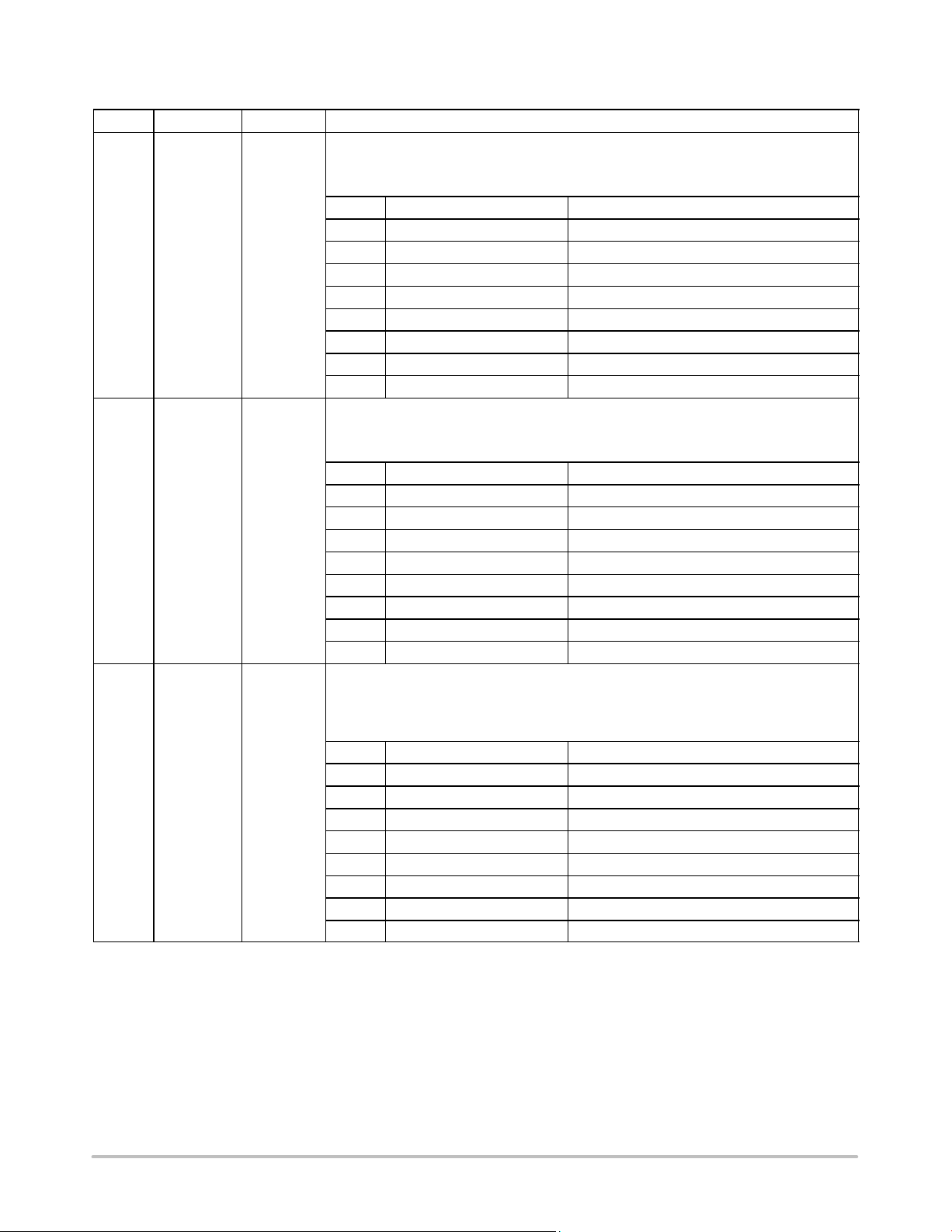
ADT7473
Table 23. Register 0x37 — Dynamic T
Bit No.
[2:0] CYR1 R/W
Mnemonic R/W Description
Control Register 2 (Power−On Default = 0x00) (Note 1)
MIN
3−bit remote 1 cycle value. These three bits define the delay time between making
subsequent T
number of monitoring cycles. The system has associated thermal time constants that need to
adjustments in the control loop for the Remote 1 channel, in terms of
MIN
be found to optimize the response of fans and the control loop.
Bits Decrease Cycle Increase Cycle
000 8 cycles (1 sec) 16 cycles (2 sec)
001 16 cycles (2 sec) 32 cycles (4 sec)
010 32 cycles (4 sec) 64 cycles (8 sec)
011 64 cycles (8 sec) 128 cycles (16 sec)
100 128 cycles (16 sec) 256 cycles (32 sec)
101 256 cycles (32 sec) 512 cycles (64 sec)
110 512 cycles (64 sec) 1024 cycles (128 sec)
111 1024 cycles (128 sec) 2048 cycles (256 sec)
[5:3] CYL R/W
3−bit local temperature cycle value. These three bits define the delay time between making
subsequent T
of number of monitoring cycles. The system has associated thermal time constants that need
adjustments in the control loop for the local temperature channel, in terms
MIN
to be found to optimize the response of fans and the control loop.
Bits Decrease Cycle Increase Cycle
000 8 cycles (1 sec) 16 cycles (2 sec)
001 16 cycles (2 sec) 32 cycles (4 sec)
010 32 cycles (4 sec) 64 cycles (8 sec)
011 64 cycles (8 sec) 128 cycles (16 sec)
100 128 cycles (16 sec) 256 cycles (32 sec)
101 256 cycles (32 sec) 512 cycles (64 sec)
110 512 cycles (64 sec) 1024 cycles (128 sec)
111 1024 cycles (128 sec) 2048 cycles (256 sec)
[7:6] CYR2 R/W
2 LSBs of 3−bit remote 2 cycle value. The MSB of the 3−bit code resides in Dynamic T
Control Register 1 (Register 0x36). These three bits define the delay time between making
subsequent T
number of monitoring cycles. The system has associated thermal time constants that need to
adjustments in the control loop for the Remote 2 channel, in terms of
MIN
MIN
be found to optimize the response of fans and the control loop.
Bits Decrease Cycle Increase Cycle
000 8 cycles (1 sec) 16 cycles (2 sec)
001 16 cycles (2 sec) 32 cycles (4 sec)
010 32 cycles (4 sec) 64 cycles (8 sec)
011 64 cycles (8 sec) 128 cycles (16 sec)
100 128 cycles (16 sec) 256 cycles (32 sec)
101 256 cycles (32 sec) 512 cycles (64 sec)
110 512 cycles (64 sec) 1024 cycles (128 sec)
111 1024 cycles (128 sec) 2048 cycles (256 sec)
1. This register becomes read−only when the Configuration Register 1 lock bit is set to 1. Any subsequent attempts to write to this register fail.
http://onsemi.com
59
Page 60
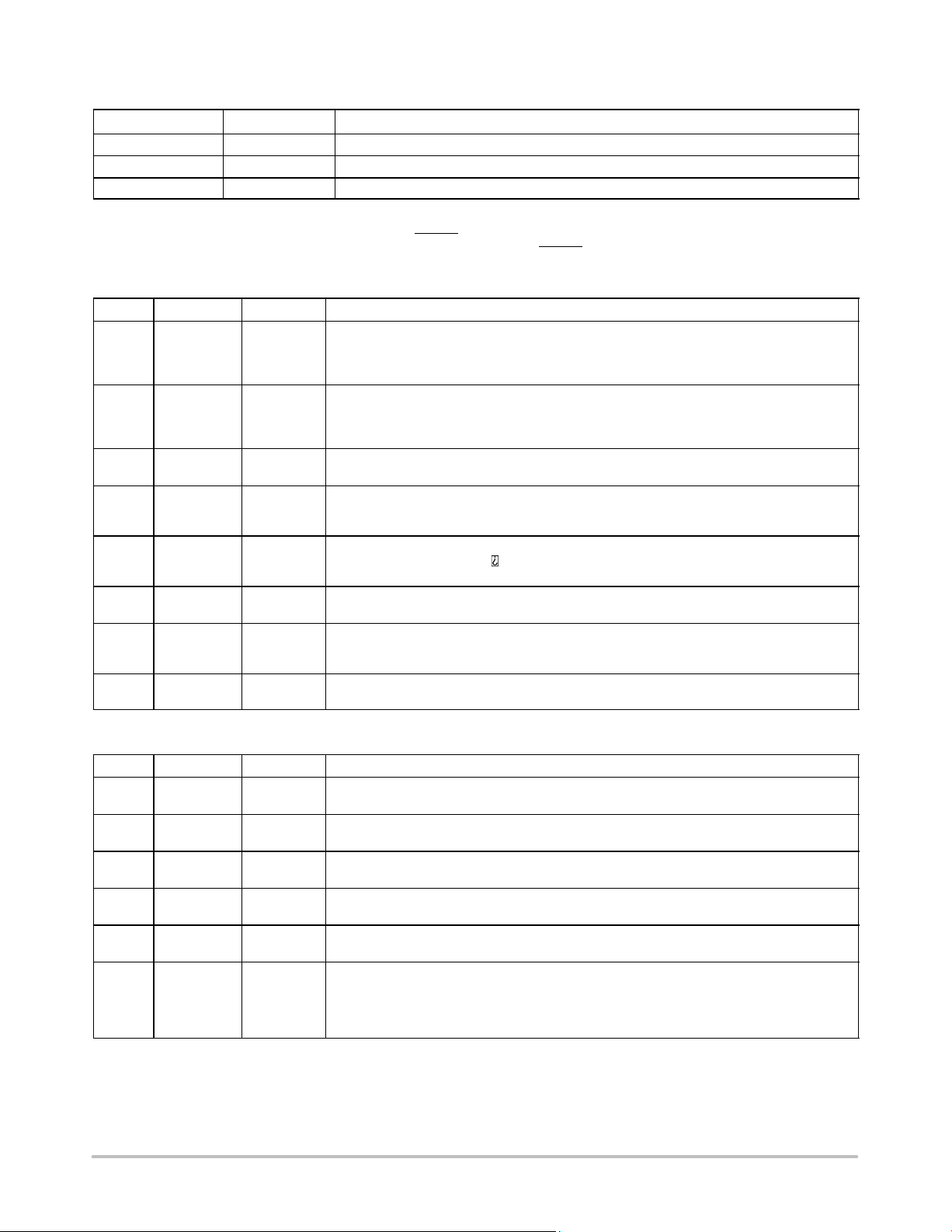
ADT7473
Table 24. Maximum PWM Duty Cycle Registers (Power−On Default = 0xFF) (Note 1, 2, and 3)
Register Address
0x38 R/W Maximum duty cycle for PWM1 output, default = 100% (0xFF).
0x39 R/W Maximum duty cycle for PWM2 output, default = 100% (0xFF).
0x3A R/W Maximum duty cycle for PWM3 output, default = 100% (0xFF).
1. These registers set the maximum PWM duty cycle of the PWM output.
2. These registers become read−only when the Configuration Register 1 lock bit is set to 1. Any subsequent attempts to write to this register fail.
3. If Bit 3 of Configuration Register 4 (0x7D) is set, then on a THERM
as programmed here. If Bit 3 of Configuration Register 4 (0x7D) is 0, then on a THERM
R/W (Note 2)
overtemperature event, fans go to their maximum programmed PWM value
Table 25. Register 0x40 — Configuration Register 1 (Power−On Default = 0x01)
Bit No. Mnemonic R/W Description
[0] STRT R/W Logic 1 enables monitoring and PWM control outputs based on the limit settings
[1] LOCK Write once Logic 1 locks all limit values to their current settings. Once this bit is set, all lockable registers
[2] RDY Read−only This bit is set to 1 by the ADT7473/ADT7473−1 to indicate only that the device is fully
[3] FSPD R/W When set to 1, this bit runs all fans at maximum speed as programmed in the maximum
[4] Vx1 R/W BIOS should set this bit to a 1 when the ADT7473/ADT7473−1 is configured to measure
[5] FSPDIS R/W Logic 1 disables fan spin−up for two TACH pulses. Instead, the PWM outputs go high for the
[6] TODIS R/W When this bit is set to 1, the SMBus timeout feature is enabled. This allows the
[7] RES
Latch Reset
programmed. Logic 0 disables monitoring and PWM control based on the default powerup
limit settings. This bit is not locked when Bit 1 (LOCK bit) has been written. This bit remains
writable after lock bit is set.
become read−only and cannot be modified until the ADT7473/ADT7473−1 is powered down
and powered up again. This prevents rogue programs, such as viruses, from modifying
critical system limit settings. (This is a lockable bit.)
powered up and ready to begin system monitoring.
PWM duty cycle registers (0x30, 0x38, 0x39 and 0x3A ). Power−on default = 0. This bit is not
locked at any time.
current from an ADI ADOPT
bit allows monitoring software to display CPU watts usage. (This is a lockable bit.)
entire fan spin−up timeout selected.
ADT7473/ADT7473−1 to be used with SMBus controllers that cannot handle SMBus
timeouts. (This is a lockable bit.)
Reserved on the ADT7473.
On the ADT7473−1, resets latch conditions when set to 1.
VRM controller and to measure the CPU’s core voltage. This
Description
overtemperature event, fans go to 100% PWM.
Table 26. Register 0x41 — Interrupt Status Register 1 (Power−On Default = 0x00)
Bit No. Mnemonic R/W Description
[1] V
[2] V
[4] R1T Read−only R1T = 1 indicates the Remote 1 low or high temperature has been exceeded. This bit is
[5] LT Read−only LT = 1 indicates the local low or high temperature has been exceeded. This bit is cleared on
[6] R2T Read−only R2T = 1 indicates the Remote 2 low or high temperature has been exceeded. This bit is
[7] OOL Read−only OOL = 1 indicates an out−of−limit event has been latched in Interrupt Status Register 2
CCP
CC
Read−only V
Read−only VCC = 1 indicates the VCC high or low limit has been exceeded. This bit is cleared on a read
= 1 indicates the V
CCP
read of the status register only if the error condition has subsided.
of the status register only if the error condition has subsided.
cleared on a read of the status register only if the error condition has subsided.
a read of the status register only if the error condition has subsided.
cleared on a read of the status register only if the error condition has subsided.
(0x42). This bit is a logical OR of all status bits in Interrupt Status Register 2. Software can
test this bit in isolation to determine whether any of the voltage, temperature, or fan speed
readings represented by Interrupt Status Register 2 are out−of−limit, which saves the need to
read Interrupt Status Register 2 every interrupt or polling cycle.
high or low limit has been exceeded. This bit is cleared on a
CCP
http://onsemi.com
60
Page 61
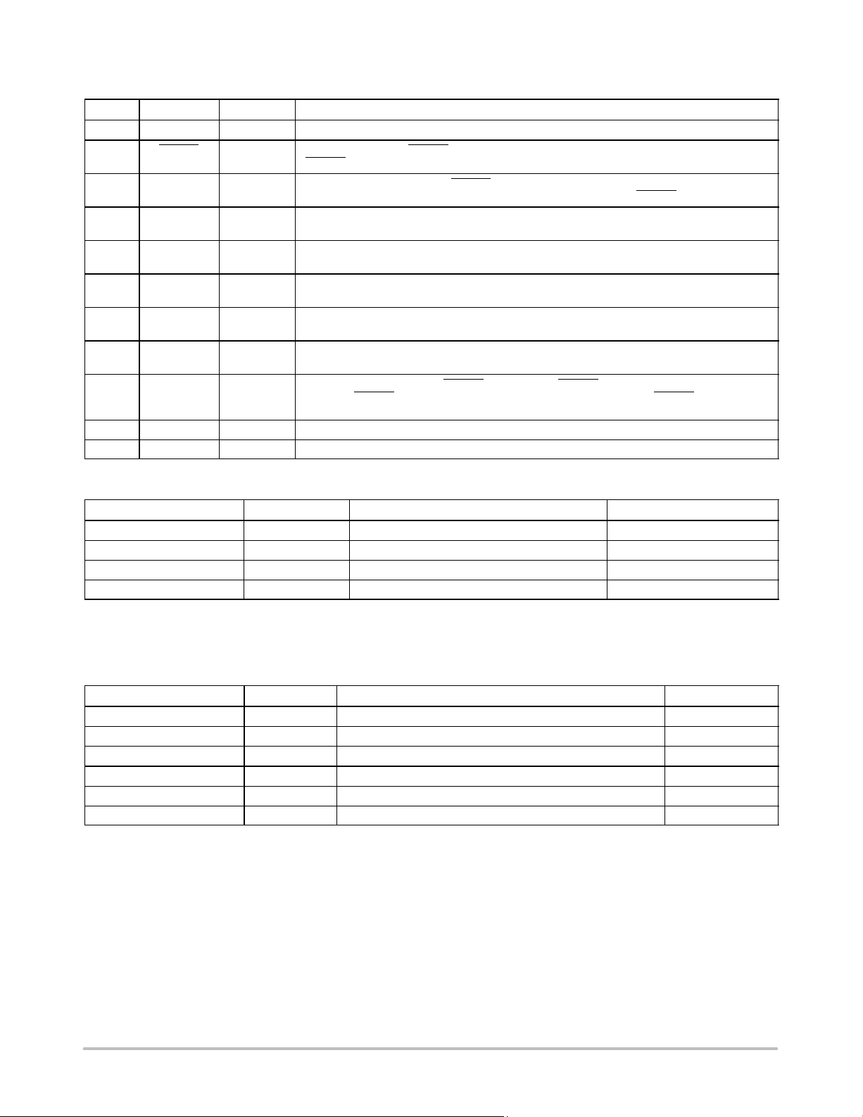
ADT7473
Table 27. Register 0x42 — Interrupt Status Register 2 (Power−On Default = 0x00)
Bit No. Mnemonic R/W Description
[0] RES Read−only Reserved on the ADT7473.
THERM
Limit Latch
[1] OVT Read−only OVT = 1 indicates one of the THERM overtemperature limits is exceeded. This bit is cleared
[2] FAN1 Read−only FAN1 = 1 indicates Fan 1 has dropped below minimum speed or has stalled. This bit is not
[3] FAN2 Read−only FAN2 = 1 indicates Fan 2 has dropped below minimum speed or has stalled. This bit is not
[4] FAN3 Read−only FAN3 = 1 indicates Fan 3 has dropped below minimum speed or has stalled. This bit is not
[5] F4P Read−only F4P = 1 indicates Fan 4 has dropped below minimum speed or has stalled. This bit is not set
R/W When Pin 9 is programmed as a GPIO output, writing to this bit determines the logic output of
Read−only If Pin 9 is configured as the THERM timer input for THERM monitoring, then this bit is set
[6] D1 Read−only D1 = 1 indicates either an open or short circuit on the Thermal Diode 1 inputs.
[7] D2 Read−only D2 = 1 indicates either an open or short circuit on the Thermal Diode 2 inputs.
On the ADT7473−1, THERM Limit Latch = 1 indicates Remote Channel 2 latch. This is a
THERM limit condition.
on a read of the status register when the temperature drops below THERM
set when the PWM1 output is off.
set when the PWM2 output is off.
set when the PWM3 output is off.
when the PWM3 output is off.
the GPIO.
when the THERM
register (Reg. 0x7A).
assertion time exceeds the limit programmed in the THERM timer limit
– T
HYST
.
Table 28. Voltage Limit Registers (Note 1)
Register Address
0x46 R/W V
0x47 R/W V
0x48 R/W VCC low limit. 0x00
0x49 R/W VCC high limit. 0xFF
1. Setting the Configuration Register 1 lock bit has no effect on these registers.
2. High limits: an interrupt is generated when a value exceeds its high limit (> comparison). Low limits: an interrupt is generated when a value
is equal to or below its low limit (≤ comparison).
R/W Description (Note 2) Power−On Default
low limit. 0x00
CCP
high limit. 0xFF
CCP
Table 29. Temperature Limit Registers (Note 1)
Register Address
0x4E R/W Remote 1 temperature low limit. 0x01
0x4F R/W Remote 1 temperature high limit. 0xFF
0x50 R/W Local temperature low limit. 0x01
0x51 R/W Local temperature high limit. 0xFF
0x52 R/W Remote 2 temperature low limit. 0x01
0x53 R/W Remote 2 temperature high limit. 0xFF
1. Exceeding any of these temperature limits by 1°C causes the appropriate status bit to be set in the interrupt status register. Setting the
Configuration Register 1 lock bit has no effect on these registers.
2. High limits: an interrupt is generated when a value exceeds its high limit (> comparison). Low limits: an interrupt is generated when a value
is equal to or below its low limit (≤ comparison).
R/W Description (Note 2) Power−On Default
http://onsemi.com
61
Page 62
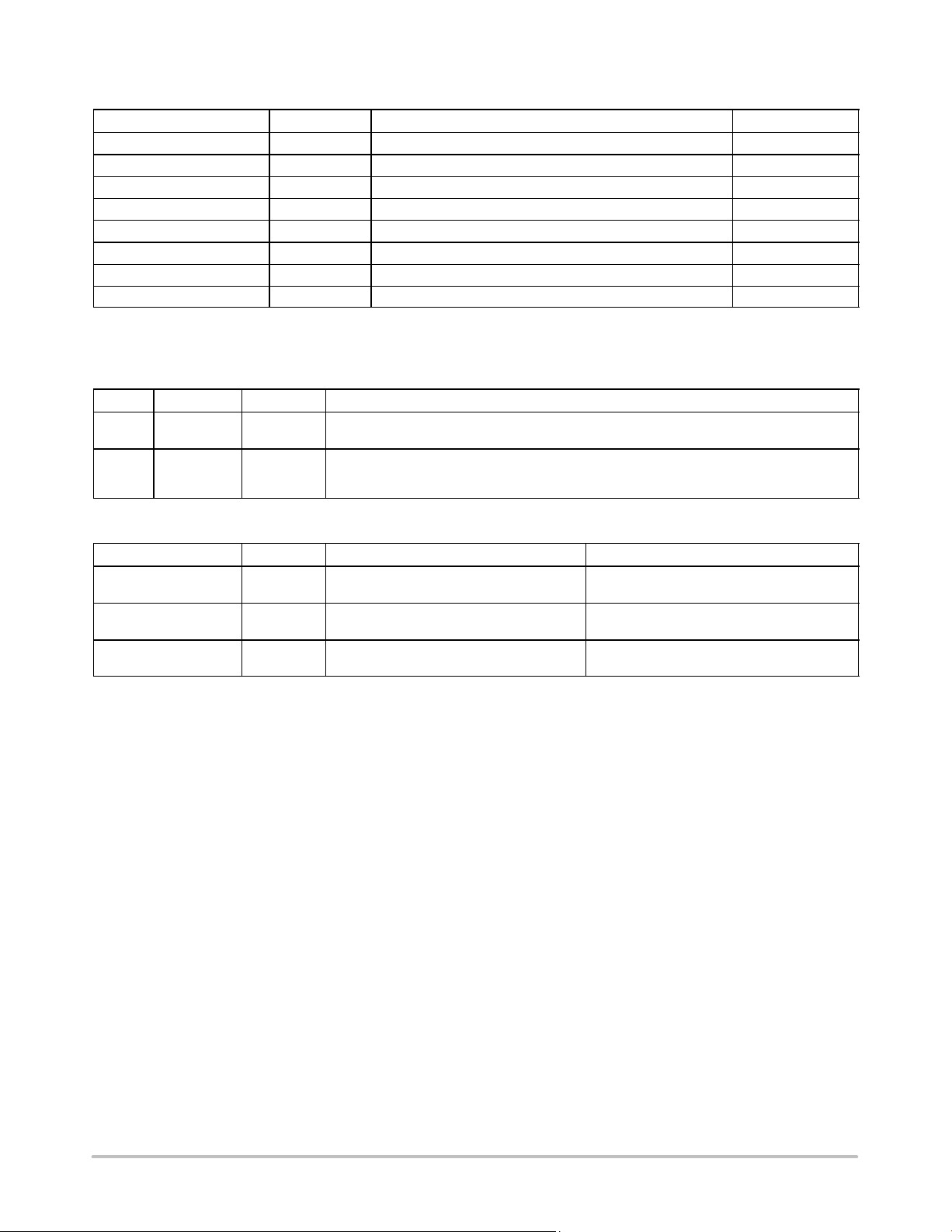
ADT7473
Table 30. Fan Tachometer Limit Registers (Note 1)
Register Address
0x54 R/W TACH1 minimum low byte. 0xFF
0x55 R/W TACH1 minimum high byte/single−channel ADC channel select. 0xFF
0x56 R/W TACH2 minimum low byte. 0xFF
0x57 R/W TACH2 minimum high byte. 0xFF
0x58 R/W TACH3 minimum low byte. 0xFF
0x59 R/W TACH3 minimum high byte. 0xFF
0x5A R/W TACH4 minimum low byte. 0xFF
0x5B R/W TACH4 minimum high byte. 0xFF
1. Exceeding any of the TACH limit registers by 1 indicates that the fan is running slowly or has stalled. The appropriate status bit is set in
Interrupt Status Register 2 to indicate the fan failure. Setting the Configuration Register 1 lock bit has no effect on these registers.
Table 31. Register 0x55 — TACH1 Minimum High Byte (Power−On Default = 0xFF)
Bit No. Mnemonic R/W Description
[4:0] Reserved Read−only These bits are reserved when Bit 6 of Configuration Register 2 (0x73) is set (single−channel
[7:5] SCADC R/W When Bit 6 of Configuration Register 2 (0x73) is set (single−channel ADC mode), these bits
R/W Description Power−On Default
ADC mode). Otherwise, these bits represent Bits [4:0] of the TACH1 minimum high byte.
are used to select the only channel from which the ADC makes measurements. Otherwise,
these bits represent Bits [7:5] of the TACH1 minimum high byte.
Table 32. PWM Configuration Registers
Register Address R/W (Note 1) Description Power−On Default
0x5C R/W PWM1 configuration. ADT7473: 0x82
0x5D R/W PWM2 configuration. ADT7473: 0x82
0x5E R/W PWM3 configuration. ADT7473: 0x82
1. These registers become read−only when the Configuration Register 1 lock bit is set. Any further attempts to write to these registers have
no effect.
ADT7473−1: 0x62
ADT7473−1: 0x62
ADT7473−1: 0x62
http://onsemi.com
62
Page 63

ADT7473
Table 33. Register 0x5C, Register 0x5D, and Register 0x5E — Configuration Registers
(ADT7473 Power−On Default = 0x82, ADT7473−1 Power−On Default = 0x62)
Bit No. Mnemonic R/W Description
[2:0] SPIN R/W
[3] SLOW R/W SLOW = 1 makes the ramp rates for acoustic enhancement four times longer.
[4] INV R/W This bit inverts the PWM output. The default is 0, which corresponds to a logic high output for
[7:5] BHVR R/W These bits assign each fan to a particular temperature sensor for localized cooling.
These bits control the startup timeout for PWMx. The PWM output stays high until two valid
TACH rising edges are seen from the fan. If there is not a valid TACH signal during the fan
TACH measurement directly after the fan startup timeout period, then the TACH
measurement reads 0xFFFF and Interrupt Status Register 2 reflects the fan fault. If the
TACH minimum high and low bytes contain 0xFFFF or 0x0000, then the Interrupt Status
Register 2 bit is not set, even if the fan has not started.
Bit Code Startup Time
000
001
010
011
100
101
110
111
100% duty cycle. Setting this bit to 1 inverts the PWM output, so 100% duty cycle
corresponds to a logic low output.
000 = Remote 1 temperature controls PWMx (automatic fan control mode).
001 = Local temperature controls PWMx (automatic fan control mode).
010 = Remote 2 temperature controls PWMx (automatic fan control mode).
011 = PWMx runs full speed (default for ADT7473−1).
100 = PWMx disabled (default for ADT7473).
101 = Fastest speed calculated by local and Remote 2 temperature controls PWMx.
110 = Fastest speed calculated by all three temperature channel controls PWMx.
111 = Manual mode. PWM duty cycle registers (Register 0x30 to Register 0x32) become
writable.
No startup timeout
100 ms
250 ms (default)
400 ms
667 ms
1 sec
2 sec
4 sec
Table 34. Temperature T
Register Address R/W (Note 1) Description Power−On Default
0x5F R/W Remote 1 T
0x60 R/W Local Temperature T
0x61 R/W Remote 2 T
1. These registers become read−only when the Configuration Register 1 lock bit is set. Any further attempts to write to these registers have
no effect.
/PWM Frequency Registers
RANGE
/PWM1 frequency. 0xCC
RANGE
/PWM2 frequency. 0xCC
RANGE
/PWM3 frequency. 0xCC
RANGE
http://onsemi.com
63
Page 64

ADT7473
Table 35. Register 0x5F, Register 0x60, and Register 0x61 — TEMP T
/PWM Frequency Registers,
RANGE
(Power−On Default = 0xCC)
Bit No. Mnemonic R/W Description
[2:0] FREQ R/W
[3] HF/LF R/W HF/LF = 1, high frequency PWM output for 4−wire fans. Once enabled, 3−wire fan−specific
[7:4] RANGE R/W
These bits control the PWMx frequency.
Bit Code Frequency
000
001
010
011
100
101
110
111
settings have no effect.
0x5F, HF/LF = 1, enables high frequency mode for Fan 1.
0x60, HF/LF = 1, enables high frequency mode for Fan 2.
0x61, HF/LF = 1, enables high frequency mode for Fan 3.
These bits determine the PWM duty cycle vs. the temperature slope for automatic fan control.
Bit Code Temperature
0000
0001
0010
0011
0100
0101
0110
0111
1000
1001
1010
1011
1100
1101
1110
1111
11.0 Hz
14.7 Hz
22.1 Hz
29.4 Hz
35.3 Hz (default)
44.1 Hz
58.8 Hz
88.2 Hz
2°C
2.5°C
3.33°C
4°C
5°C
6.67°C
8°C
10°C
13.33°C
16°C
20°C
26.67°C
32°C (default)
40°C
53.33°C
80°C
http://onsemi.com
64
Page 65

ADT7473
Table 36. Register 0x62 — Enhanced Acoustics Register 1 (Power−On Default = 0x00)
Bit No. Mnemonic R/W (Note 1) Description
[2:0] ACOU R/W
[3] EN1 R/W When this bit is 1, acoustic enhancement is enabled on PWM1 output.
[4] SYNC R/W SYNC = 1 synchronizes fan speed measurements on TACH2, TACH3, and TACH4 to PWM3.
[5] MIN1 R/W When the ADT7473/ADT7473−1 is in automatic fan control mode, this bit defines whether
[6] MIN2 R/W When the ADT7473/ADT7473−1 is in automatic fan speed control mode, this bit defines
[7] MIN3 R/W When the ADT7473/ADT7473−1 is in automatic fan speed control mode, this bit defines
1. This register becomes read−only when the Configuration Register 1 lock bit is set to 1. Any further attempts to write to this register have
no effect.
These bits select the ramp rate applied to the PWM1 output. Instead of PWM1 jumping
instantaneously to its newly calculated speed, PWM1 ramps gradually at the rate determined
by these bits. This feature enhances the acoustics of the fan being driven by the PWM1
output.
Time Slot Increase Time for 33% to 100%
000 = 1
001 = 2
010 = 3
011 = 4
100 = 8
101 = 12
110 = 24
111 = 48
35 sec
17.6 sec
11.8 sec
7.0 sec
4.4 sec
3.0 sec
1.6 sec
0.8 sec
This allows up to three fans to be driven from PWM3 output and their speeds to be measured.
SYNC = 0 synchronizes only TACH3 and TACH4 to PWM3 output.
PWM1 is off (0% duty cycle) or at PWM1 minimum duty cycle when the controlling
temperature is below its T
0 = 0% duty cycle below T
1 = PWM1 minimum duty cycle below T
– hysteresis value.
MIN
− hysteresis.
MIN
− hysteresis.
MIN
whether PWM2 is off (0% duty cycle) or at PWM2 minimum duty cycle when the controlling
temperature is below its T
0 = 0% duty cycle below T
1 = PWM 2 minimum duty cycle below T
− hysteresis value.
MIN
− hysteresis.
MIN
− hysteresis.
MIN
whether PWM3 is off (0% duty cycle) or at PWM3 minimum duty cycle when the controlling
temperature is below its T
0 = 0% duty cycle below T
1 = PWM3 minimum duty cycle below T
− hysteresis value.
MIN
− hysteresis.
MIN
− hysteresis.
MIN
http://onsemi.com
65
Page 66
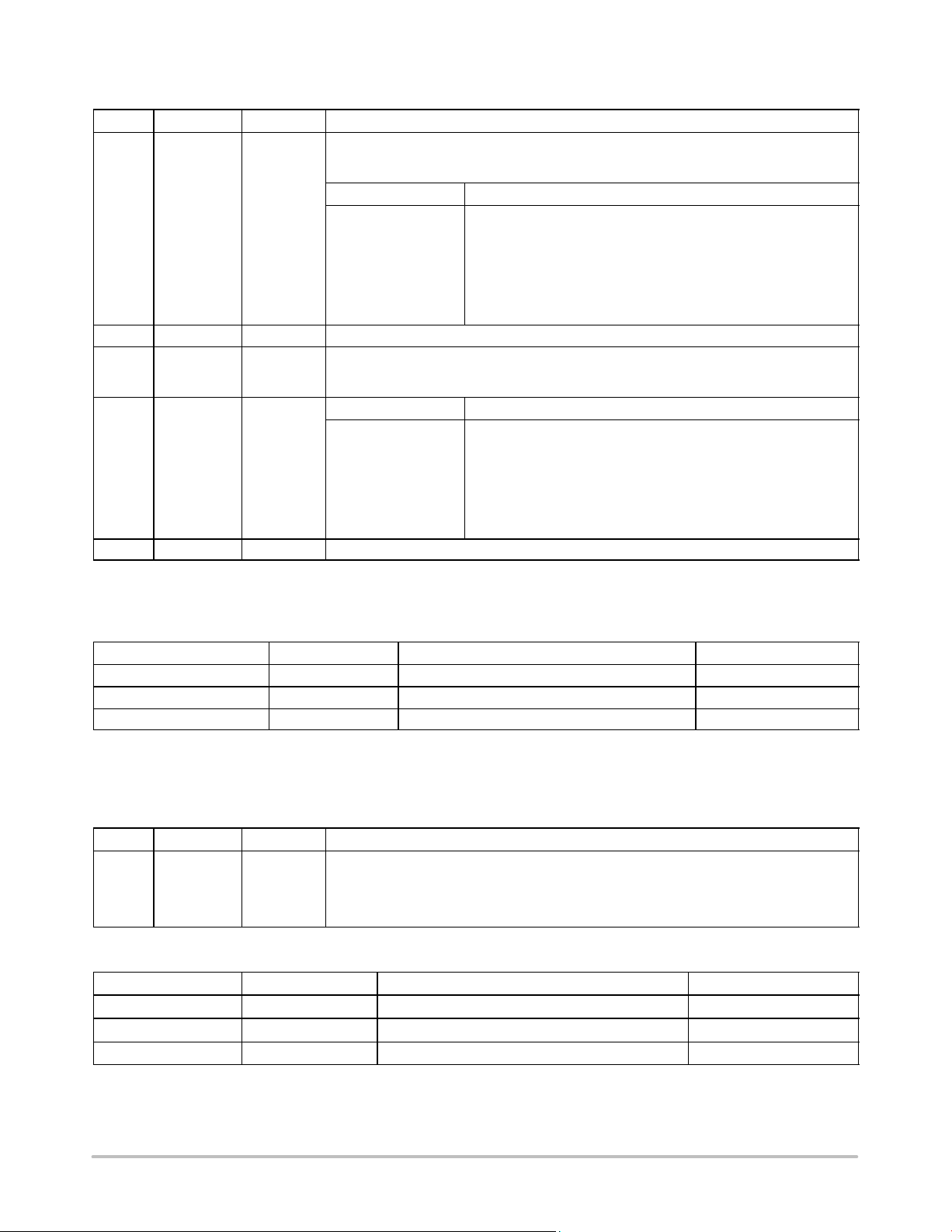
ADT7473
Table 37. Register 0x63 — Enhanced Acoustics Register 2 (Power−On Default = 0x00)
Bit No. Mnemonic R/W (Note 1) Description
[2:0] ACOU3 R/W
[3] EN3 R/W When this bit is 1, acoustic enhancement is enabled on PWM3 output.
[6:4] ACOU2 R/W These bits select the ramp rate applied to the PWM2 output. Instead of PWM2 jumping
[7] EN2 R/W When this bit is 1, acoustic enhancement is enabled on PWM2 output.
1. This register becomes read−only when the Configuration Register 1 lock bit is set to 1. Any further attempts to write to this register have
no effect.
These bits select the ramp rate applied to the PWM3 output. Instead of PWM3 jumping
instantly to its newly calculated speed, PWM3 ramps gradually at the rate determined by
these bits. This effect enhances the acoustics of the fan being driven by the PWM3 output.
Time Slot Increase Time for 33% to 100%
000 = 1
001 = 2
010 = 3
011 = 4
100 = 8
101 = 12
110 = 24
111 = 48
instantly to its newly calculated speed, PWM2 ramps gradually at the rate determined by
these bits. This effect enhances the acoustics of the fans being driven by the PWM2 output.
Time Slot Increase Time for 33% to 100%
000 = 1
001 = 2
010 = 3
011 = 4
100 = 8
101 = 12
110 = 24
111 = 48
35 sec
17.6 sec
11.8 sec
7.0 sec
4.4 sec
3.0 sec
1.6 sec
0.8 sec
35 sec
17.6 sec
11.8 sec
7.0 sec
4.4 sec
3.0 sec
1.6 sec
0.8 sec
Table 38. PWM Minimum Duty Cycle Registers
Register Address R/W (Note 1) Description Power−On Default
0x64 R/W PWM1 minimum duty cycle. 0x80 (50% duty cycle)
0x65 R/W PWM2 minimum duty cycle. 0x80 (50% duty cycle)
0x66 R/W PWM3 minimum duty cycle. 0x80 (50% duty cycle)
1. These registers become read−only when the Configuration Register 1 lock bit is set. Any further attempts to write to these registers have
no effect.
Table 39. Register 0x64, Register 0x65, and Register 0x66 — PWM Minimum Duty Cycle Registers
(Power−On Default = 0x80, 50% Duty Cycle)
Bit No. Mnemonic R/W Description
[7:0] PWM Duty
Table 40. T
Register Address
Cycle
Registers (Note 1)
MIN
0x67
0x68
0x69
1. These are the T
minimum speed and increases with temperature according to T
2. These registers become read−only when the Configuration Register 1 lock bit is set. Any further attempts to write to these registers have
no effect.
registers for each temperature channel. When the temperature measured exceeds T
MIN
R/W These bits define the PWM
0x00 = 0% duty cycle (fan off).
0x40 = 25% duty cycle.
0x80 = 50% duty cycle.
0xFF = 100% duty cycle (fan full speed).
R/W (Note 2) Description Power−On Default
R/W Remote 1 temperature T
R/W Local temperature T
R/W Remote 2 temperature T
duty cycle for PWMx.
MIN
MIN
. 0x9A (90°C)
MIN
MIN
.
RANGE
. 0x9A (90°C)
. 0x9A (90°C)
, the appropriate fan runs at
MIN
http://onsemi.com
66
Page 67
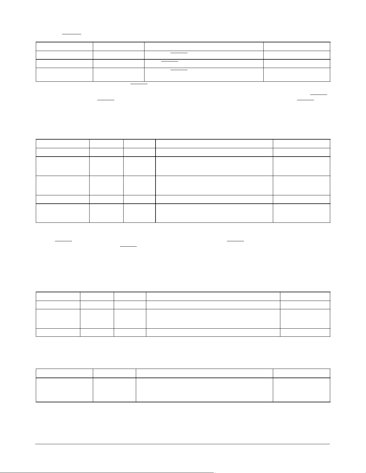
ADT7473
Table 41. THERM Limit Registers (Note 1)
Register Address
0x6A R/W Remote 1 THERM limit. 0xA4 (100°C)
0x6B R/W Local THERM limit. 0xA4 (100°C)
0x6C R/W Remote 2 THERM limit. ADT7473: 0xA4 (100°C)
1. If any temperature measured exceeds its THERM limit, all PWM outputs drive their fans at 100% duty cycle. This is a fail−safe mechanism
incorporated to cool the system in the event of a critical overtemperature. It also ensures some level of cooling in the event that software
or hardware locks up. If set to 0x80, this feature is disabled. The PWM output remains at 100% until the temperature drops below THERM
Limit − Hysteresis. If the THERM pin is programmed as an output, then exceeding these limits by 0.25°C can cause the THERM pin to
assert low as an output.
2. These registers become read−only when the Configuration Register 1 lock bit is set to 1. Any further attempts to write to these registers
have no effect.
R/W (Note 2) Description Power−On Default
ADT7473−1: 0xC8 (136°C)
Table 42. Temperature/T
Register Address
Hysteresis Registers (Note 1)
MIN
Bit Name R/W (Note 2) Description Power−On Default
0x6D R/W Remote 1 and local temperature hysteresis. 0x44
HYSL [3:0] Local temperature hysteresis. 0°C to 15°C of
hysteresis can be applied to the local temperature
AFC and dynamic T
control loops.
MIN
HYSR1 [7:4] Remote 1 temperature hysteresis. 0°C to 15°C of
hysteresis can be applied to the Remote 1
temperature AFC and dynamic T
control loops.
MIN
0x6E R/W Remote 2 temperature hysteresis. 0x40
HYSR2 [7:4] Local temperature hysteresis. 0°C to 15°C of
hysteresis can be applied to the local temperature
AFC and dynamic T
control loops.
MIN
1. Each 4−bit value controls the amount of temperature hysteresis applied to a particular temperature channel. Once the temperature for
that channel falls below its T
15°C of hysteresis can be assigned to any temperature channel. The hysteresis value chosen also applies to that temperature channel,
if its THERM
limit is exceeded. The PWM output being controlled goes to 100%, if the THERM limit is exceeded and remains at 100%
until the temperature drops below THERM
value, the fan remains running at PWM
MIN
– hysteresis. For acoustic reasons, it is recommended that the hysteresis value not be
duty cycle until the temperature = T
MIN
– hysteresis. Up to
MIN
programmed less than 4°C. Setting the hysteresis value lower than 4°C causes the fan to switch on and off regularly when the temperature
is close to T
2. These registers become read−only when the Configuration Register 1 lock bit is set to 1. Any further attempts to write to these registers
MIN
.
have no effect.
Table 43. XNOR Tree Test Register
Register Address Bit Name R/W (Note 1) Description Power−On Default
0x6F R/W XNOR tree test enable register. 0x00
XEN [0] If the XEN bit is set to 1, the device enters the XNOR tree
Res [7:1] Unused. Do not write to these bits.
1. These registers become read−only when the Configuration Register 1 lock bit is set to 1. Any further attempts to write to these registers
have no effect.
test mode. Clearing the bit removes the device from the
XNOR tree test mode.
Table 44. Remote 1 Temperature Offset Register (0x70)
Register Address R/W (Note 1) Description Power−On Default
[7:0] R/W Allows a twos complement offset value to be automatically
0x00
added to or subtracted from the Remote 1 temperature
reading. This is to compensate for any inherent system
offsets such as PCB trace resistance. LSB value = 0.5°C.
1. This register becomes read−only when the Configuration Register 1 lock bit is set to 1. Any further attempts to write to this register have
no effect.
http://onsemi.com
67
Page 68

ADT7473
Table 45. Local Temperature Offset Register (0x71)
Register Address R/W (Note 1) Description Power−On Default
[7:0] R/W Allows a twos complement offset value to be automatically
1. This register becomes read−only when the Configuration Register 1 lock bit is set to 1. Any further attempts to write to this register have
no effect.
added to or subtracted from the local temperature reading.
LSB value = 0.5°C.
Table 46. Remote 2 Temperature Offset Register (0x72)
Register Address R/W (Note 1) Description Power−On Default
[7:0] R/W Allows a twos complement offset value to be automatically
1. This register becomes read−only when the Configuration Register 1 lock bit is set to 1. Any further attempts to write to this register have
no effect.
added to or subtracted from the Remote 2 temperature
reading. This is to compensate for any inherent system
offsets such as PCB trace resistance. LSB value = 0.5°C.
Table 47. Register 0x73 — Configuration Register 2 (Power−On Default = 0x00)
Bit No. Mnemonic R/W (Note 1) Description
0 FanPresDT R/W When FanPresenceDT = 1, the state of Bits [3:1] of Register 0x73 reflects the presence of a
1 Fan1Detect Read−only Fan1 Detect = 1 indicates a 4−wire fan is connected to the PWM1 input.
2 Fan2Detect Read−only Fan1 Detect = 1 indicates a 4−wire fan is connected to the PWM2 input.
3 Fan3Detect Read−only Fan1 Detect = 1 indicates a 4−wire fan is connected to the PWM3 input.
4 AV G R/W AVG = 1, averaging on the temperature and voltage measurements is turned off. This allows
5 ATTN R/W ATTN = 1, the ADT7473/ADT7473−1 removes the attenuators from the V
6 CONV R/W
7 Shutdown R/W SHDN = 1, ADT7473/ADT7473−1 goes into shutdown mode. All PWM outputs assert low or
1. This register becomes read−only when the Configuration Register 1lock bit is set to 1. Any further attempts to write to this register have
no effect.
4−wire fan on the appropriate TACH channel.
measurements on each channel to be made much faster.
V
input can be used for other functions such as connecting up external sensors.
CCP
CONV = 1, the ADT7473/ADT7473−1 is put into a single−channel ADC conversion mode. In
this mode, the ADT7473/ADT7473−1 can be made to read continuously from one input only,
for example, Remote 1 temperature. The appropriate ADC channel is selected by writing to
Bits [7:5] of TACH1 minimum high byte register (0x55).
Bits [7:5], Register 0x55
000
001
010
011
100
101
110
111
high, depending on the state of the INV bit, to switch off all fans.
Reserved
V
CCP
VCC (3.3V)
Reserved
Reserved
Remote 1 temperature
Local temperature
Remote 2 temperature
input. The
CCP
0x00
0x00
http://onsemi.com
68
Page 69
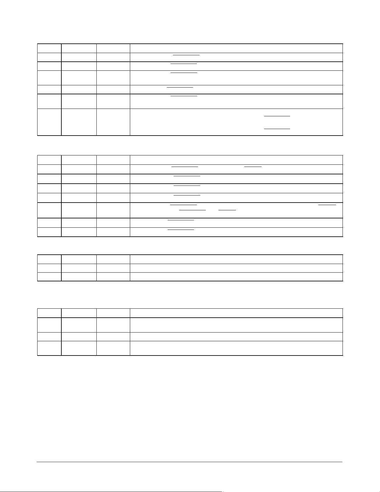
ADT7473
Table 48. Register 0x74 — Interrupt Mask Register 1 (Power−On Default = 0x00)
Bit No. Mnemonic R/W Description
[1] V
[2] V
CCP
CC
[4] R1T R/W R1T = 1, masks SMBALERT for out−of−limit conditions on the Remote 1 temperature
[5] LT R/W LT = 1, masks SMBALERT for out−of−limit conditions on the local temperature channel.
[6] R2T R/W R2T = 1, masks SMBALERT for out−of−limit conditions on the Remote 2 temperature
[7] OOL R/W OOL = 0, then when one or more alerts are generated in Interrupt Status Register 2, assuming
Table 49. Register 0x75 — Interrupt Mask Register 2 (Power−On Default <7:0> = 0x00)
Bit No. Mnemonic R/W Description
[1] OVT R/W OVT = 1, masks SMBALERT for overtemperature THERM conditions.
[2] FAN1 R/W FAN1 = 1, masks SMBALERT for a Fan 1 fault.
[3] FAN2 R/W FAN2 = 1, masks SMBALERT for a Fan 2 fault.
[4] FAN3 R/W FAN3 = 1, masks SMBALERT for a Fan 3 fault.
[5] F4P R/W F4P = 1, masks SMBALERT for a Fan 4 fault. If the TACH4 pin is being used as the THERM
[6] D1 R/W D1 = 1, masks SMBALERT for a diode open or short on a Remote 1 channel.
[7] D2 R/W D2 = 1, masks SMBALERT for a diode open or short on a Remote 2 channel.
R/W V
= 1, masks SMBALERT for out−of−limit conditions on the V
CCP
R/W VCC = 1, masks SMBALERT for out−of−limit conditions on the V
channel.
channel.
all the mask bits in the Interrupt Mask Register 2 (0x75) = 1, SMBALERT
OOL = 1, then when one or more alerts are generated in Interrupt Status Register 2, assuming
all the mask bits in the Interrupt Mask Register 2 (0x75) = 1, SMBALERT
input, this bit masks SMBALERT for a THERM timer event.
channel.
CCP
channel.
CC
are still asserted.
are not asserted.
Table 50. Register 0x76 — Extended Resolution Register 1 (Power−On Default = 0x00) (Note 1)
Bit No.
[3:2] V
[5:4] V
1. If this register is read, this register and the registers holding the MSB of each reading are frozen until read.
Mnemonic R/W Description
CCP
CC
Read−only V
Read−only VCC LSBs. Holds the 2 LSBs of the 10−bit VCC measurement.
LSBs. Holds the 2 LSBs of the 10−bit V
CCP
measurement.
CCP
Table 51. Register 0x77 — Extended Resolution Register 2 (Power−On Default = 0x00) (Note 1)
Bit No.
[3:2] TDM1 Read−only Remote 1 temperature LSBs. Holds the 2 LSBs of the 10−bit Remote 1 temperature
[5:4] LTMP Read−only Local temperature LSBs. Holds the 2 LSBs of the 10−bit local temperature measurement.
[7:6] TDM2 Read−only Remote 2 temperature LSBs. Holds the 2 LSBs of the 10−bit Remote 2 temperature
1. If this register is read, this register and the registers holding the MSB of each reading are frozen until read.
Mnemonic R/W Description
measurement.
measurement.
http://onsemi.com
69
Page 70
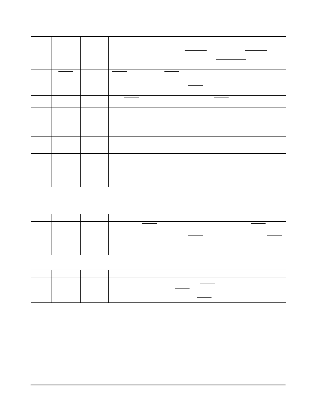
ADT7473
Table 52. Register 0x78 — Configuration Register 3 (Power−On Default = 0x00)
Bit No. Mnemonic R/W (Note 1) Description
[0] ALERT
Enable
[1] THERM R/W THERM Enable = 1 enables THERM functionality on Pin 9. Also determined by Bit 0 and
[2] BOOST R/W When THERM is an input and BOOST = 1, assertion of THERM causes all fans to run at the
[3] FAST R/W FAST = 1, enables fast TACH measurements on all channels. This increases the TACH
[4] DC1 R/W DC1 = 1, enables TACH measurements to be continuously made on TACH1. Fans must be
[5] DC2 R/W DC2 = 1, enables TACH measurements to be continuously made on TACH2. Fans must be
[6] DC3 R/W DC3 = 1, enables TACH measurements to be continuously made on TACH3. Fans must be
[7] DC4 R/W DC4 = 1, enables TACH measurements to be continuously made on TACH4. Fans must be
1. This register becomes read−only when the Configuration Register 1 lock bit is set to 1. Any further attempts to write to this register have
no effect.
R/W ALERT = 0 (default), ADT7473 Pin 5 is configured as PWM2.
ALERT = 1, Pin 5 for ADT7473 (PWM2/SMBALERT
interrupt output to indicate out−of−limit error conditions.
ALERT = 0 (default), ADT7473−1 Pin 5 is configured as. THERM_LATCH.
ALERT = 1, Pin 5 for ADT7473−1 (THERM_LATCH/PWM2) is configured as PWM2.
Bit 1 (PIN9FUNC) of Configuration Register 4. Direction is controlled by Bit 5, Bit 6, and Bit 7
of Configuration Register 5 (0x7C). When THERM
boost bit is set, the fans run at full speed. THERM can also be programmed so that a timer
monitors the duration THERM has been asserted.
maximum programmed duty cycle for fail−safe cooling.
measurement rate from once per second to once every 250 ms (4 x).
driven by dc. Setting this bit prevents pulse stretching because it is not required for dc−driven
motors.
driven by dc. Setting this bit prevents pulse stretching because it is not required for dc−driven
motors.
driven by dc. Setting this bit prevents pulse stretching because it is not required for dc−driven
motors.
driven by dc. Setting this bit prevents pulse stretching because it is not required for dc−driven
motors.
) is configured as an SMBALERT
is asserted, if the fans are running and the
Table 53. Register 0x79 — THERM Timer Status Register (Power−On Default = 0x00)
Bit No. Mnemonic R/W Description
[7:1] TMR R Times how long THERM input is asserted. These seven bits read 0 until the THERM
[0] ASRT/
TMR0
R This bit is set high on the assertion of the THERM input and is cleared on read. If the THERM
assertion time exceeds 45.52 ms.
assertion time exceeds 45.52 ms, this bit is set and becomes the LSB of the 8−bit TMR
reading. This allows THERM assertion times from 45.52 ms to 5.82 sec to be reported back
with a resolution of 22.76 ms.
Table 54. Register 0x7A — THERM Timer Limit Register (Power−On Default = 0x00)
Bit No. Mnemonic R/W Description
[7:0] LIMT R/W Sets maximum THERM assertion length allowed before an interrupt is generated. This is an
8−bit limit with a resolution of 22.76 ms allowing THERM
seconds to be programmed. If the THERM assertion time exceeds this limit, Bit 5 (F4P) of
Interrupt Status Register 2 (Reg. 0x42) is set. If the limit value is 0x00, an interrupt is
generated immediately on the assertion of the THERM input.
assertion limits of 45.52 ms to 5.82
http://onsemi.com
70
Page 71

ADT7473
Table 55. Register 0x7B — TACH Pulses per Revolution Register (Power−On Default = 0x55)
Bit No. Mnemonic R/W Description
[1:0] FAN1 R/W
[3:2] FAN2 R/W
[5:4] FAN3 R/W
[7:6] FAN4 R/W
Sets number of pulses to be counted when measuring Fan 1 speed. Can be used to
determine fan pulses per revolution for unknown fan type.
Bit Code Pulses Counted
00
01
10
11
Sets number of pulses to be counted when measuring Fan 2 speed. Can be used to
determine fan pulses per revolution for unknown fan type.
Bit Code Pulses Counted
00
01
10
11
Sets number of pulses to be counted when measuring Fan 3 speed. Can be used to
determine fan pulses per revolution for unknown fan type.
Bit Code Pulses Counted
00
01
10
11
Sets number of pulses to be counted when measuring Fan 4 speed. Can be used to
determine fan pulses per revolution for unknown fan type.
Bit Code Pulses Counted
00
01
10
11
1
2 (default)
3
4
1
2 (default)
3
4
1
2 (default)
3
4
1
2 (default)
3
4
http://onsemi.com
71
Page 72
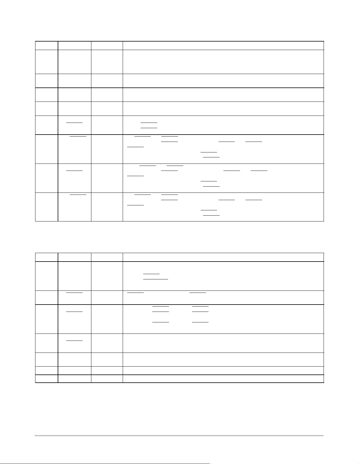
ADT7473
Table 56. Register 0x7C — Configuration Register 5 (ADT7473Power−On Default = 0x00)
Bit No. Mnemonic R/W (Note 1) Description
[0] TWOS
COMPL
[1] Temp Offset TempOffset = 0 sets offset range to ±64°C at 0.5°C resolution.
[2] GPIOD GPIO direction. When GPIO function is enabled, this determines whether the GPIO is an
[3] GPIOP GPIO polarity. When the GPIO function is enabled and is programmed as an output, this bit
[4] RES
THERM
Hysteresis
[5] R1 THERM R/W R1 THERM = 1, THERM temperature limit functionality enabled for Remote 1 temperature
[6] Local
THERM
[7] R2 THERM R/W R2 THERM = 1, THERM temperature limit functionality enabled for Remote 2 temperature
1. This register becomes read−only when the Configuration Register 1 lock bit is set to 1. Any further attempts to write to this register have
no effect.
R/W Twos complement = 1, sets the temperature range to twos complement temperature range.
R/W Reserved on the ADT7473 On the ADT7473−1:
R/W Local THERM = 1, THERM temperature limit functionality enabled for the local temperature
Twos complement = 0, changes the temperature range to Offset 64. When this bit is
changed, the ADT7473/ADT7473−1 interprets all relevant temperature register values as
defined by this bit.
TempOffset = 1 sets offset range to ±128°C at 1°C resolution.
input (0) or an output (1).
determines whether the GPIO is active low (0) or high (1).
0 = THERM
1 = THERM hysteresis enabled
channel; that is, THERM
THERM can also be disabled on any channel by:
Writing −64°C to the appropriate THERM temperature limit in Offset 64 mode.
Writing −128°C to the appropriate THERM temperature limit in twos complement mode.
channel; that is, THERM
THERM can also be disabled on any channel by:
Writing −64°C to the appropriate THERM temperature limit in Offset 64 mode.
Writing −128°C to the appropriate THERM temperature limit in twos complement mode.
channel; that is, THERM
THERM can also be disabled on any channel by:
Writing −64°C to the appropriate THERM temperature limit in Offset 64 mode.
Writing −128°C to the appropriate THERM temperature limit in twos complement mode.
hysteresis disabled
is bidirectional. R1 THERM = 0, THERM is a timer input only.
is bidirectional. Local THERM = 0, THERM is a timer input only.
is bidirectional. R2 THERM = 0, THERM is a timer input only.
Table 57. Register 0x7D — Configuration Register 4 (Power−On Default = 0x00)
Bit No. Mnemonic R/W (Note 1) Description
[1:0] Pin9FUNC R/W These bits set the functionality of Pin 9.
[2] THERM
[3] Max/Full on
[4] RES
[5] BpAttV
[6] RES Reserved
[7] RES Reserved
1. This register becomes read−only when the Configuration Register 1 lock bit is set to 1. Any further attempts to write to this register have
no effect.
Disable
THERM
THERM
Config
CCP
R/W THERM Disable = 1, disables THERM overtemperature output features.
R/W Max/Full on THERM = 0; when THERM temperature limit is exceeded, fans go to full speed.
R/W Bypass V
00 = TACH4 (default)
01 = THERM
10 = SMBALERT
11 = GPIO
Max/Full on THERM
programmed fan speed.
Max/Full on THERM = 1; when THERM limit is exceeded, fans go to maximum speed as
defined in Register 0x38, Register 0x39, Register 0x3A.
Unused on ADT7473. On the ADT7473−1:
0 = Remote Channel 2 (default)
1 = Remote Channel 1 and Remote Channel 2
0 V (0x00) to 2.2965 V (0xFF).
CCP
= 1; when THERM temperature limit is exceeded, fans go to maximum
attenuator. When set, the measurement scale for this channel changes from
http://onsemi.com
72
Page 73
ADT7473
Table 58. Register 0x7E — Manufacturer’s Test Register 1 (Power−On Default = 0x00)
Bit No. Mnemonic R/W Description
[7:0] Reserved Read−only Manufacturer’s test register. These bits are reserved for manufacturer’s test purposes and
Table 59. Register 0x7F — Manufacturer’s Test Register 2 (Power−On Default = 0x00)
Bit No. Mnemonic R/W Description
[7:0] Reserved Read−only Manufacturer’s test register. These bits are reserved for manufacturer’s test purposes and
Table 60. Register 0x80 — Manufacturer’s Test Register 3 (Power−On Default = 0x10)
Bit No. Mnemonic R/W Description
[7:0] Reserved Read−only Manufacturer’s test register. These bits are reserved for manufacturer’s test purposes and
ORDERING INFORMATION
Device Order Number* Package Type Package Option Shipping
ADT7473ARQZ
ADT7473ARQZ−REEL 2500 Tape & Reel
ADT7473ARQZ−RL7 1000 Tape & Reel
ADT7473ARQZ−001 98 Tube
ADT7473ARQZ−1RL 2500 Tape & Reel
ADT7473ARQZ−1R7 1000 Tape & Reel
†For information on tape and reel specifications, including part orientation and tape sizes, please refer to our Tape and Reel Packaging
Specifications Brochure, BRD8011/D.
*These are Pb−Free packages.
should not be written to under normal operation.
should not be written to under normal operation.
should not be written to under normal operation.
†
98 Tube
16−Lead QSOP RQ−16
http://onsemi.com
73
Page 74
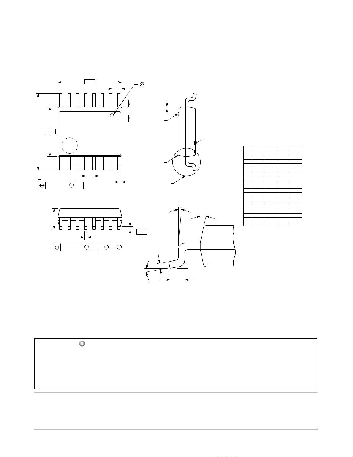
ADT7473
PACKAGE DIMENSIONS
QSOP16
CASE 492−01
ISSUE O
−B−
L
0.25 (0.010) T
C
D
16 PL
0.25 (0.010) T BA
−A−
R
U
G
M
K
P
Q
H x 45
RAD.
0.013 X 0.005
DP. MAX
RAD.
0.005−0.010
TYP
DETAIL E
NOTES:
1. DIMENSIONING AND TOLERANCING PER ANSI
Y14.5M, 1982.
_
MOLD PIN
MARK
V
N
2. CONTROLLING DIMENSION: INCH.
3. THE BOTTOM PACKAGE SHALL BE BIGGER THAN
THE TOP PACKAGE BY 4 MILS (NOTE: LEAD SIDE
ONLY). BOTTOM PACKAGE DIMENSION SHALL
FOLLOW THE DIMENSION STATED IN THIS
DRAWING.
4. PLASTIC DIMENSIONS DOES NOT INCLUDE MOLD
FLASH OR PROTRUSIONS. MOLD FLASH OR
PROTRUSIONS SHALL NOT EXCEED 6 MILS PER
SIDE.
5. BOTTOM EJECTOR PIN WILL INCLUDE THE
COUNTRY OF ORIGIN (COO) AND MOLD CAVITY I.D.
INCHES
DIM MINMAXMIN
A 4.80 4.980.189 0.196
B 3.81 3.990.150 0.157
C 1.55 1.730.061 0.068
D 0.20 0.310.008 0.012
F 0.41 0.890.016 0.035
G 0.64 BSC0.025 BSC
H 0.20 0.460.008 0.018
J 0.249 0.1910.0098 0.0075
K 0.10 0.250.004 0.010
L 5.84 6.200.230 0.244
8 PL
M 0 8 0
N 0 7 0 7
P 0.18 0.280.007 0.011
Q 0.51 DIA0.020 DIA
R 0.64 0.890.025 0.035
U 0.64 0.890.025 0.035
V
8
_
8
_
MILLIMETERS
MAX
___
____
0 8 0
___
−T−
SEATING
PLANE
M
S S
J
M
F
DETAIL E
dBCOOL is a registered trademarks of Semiconductor Components Industries, LLC (SCILLC). Pentium is a registered trademark of Intel Corporation.
ON Semiconductor and are registered trademarks of Semiconductor Components Industries, LLC (SCILLC). SCILLC reserves the right to make changes without further notice
to any products herein. SCILLC makes no warranty, representation or guarantee regarding the suitability of its products for any particular purpose, nor does SCILLC assume any liability
arising out of the application or use of any product or circuit, and specifically disclaims any and all liability, including without limitation special, consequential or incidental damages.
“Typical” parameters which may be provided in SCILLC data sheets and/or specifications can and do vary in different applications and actual performance may vary over time. All
operating parameters, including “Typicals” must be validated for each customer application by customer’s technical experts. SCILLC does not convey any license under its patent rights
nor the rights of others. SCILLC products are not designed, intended, or authorized for use as components in systems intended for surgical implant into the body, or other applications
intended to support or sustain life, or for any other application in which the failure of the SCILLC product could create a situation where personal injury or death may occur. Should
Buyer purchase or use SCILLC products for any such unintended or unauthorized application, Buyer shall indemnify and hold SCILLC and its officers, employees, subsidiaries, affiliates,
and distributors harmless against all claims, costs, damages, and expenses, and reasonable attorney fees arising out of, directly or indirectly, any claim of personal injury or death
associated with such unintended or unauthorized use, even if such claim alleges that SCILLC was negligent regarding the design or manufacture of the part. SCILLC is an Equal
Opportunity/Affirmative Action Employer. This literature is subject to all applicable copyright laws and is not for resale in any manner.
PUBLICATION ORDERING INFORMATION
LITERATURE FULFILLMENT:
Literature Distribution Center for ON Semiconductor
P.O. Box 5163, Denver, Colorado 80217 USA
Phone: 303−675−2175 or 800−344−3860 Toll Free USA/Canada
Fax: 303−675−2176 or 800−344−3867 Toll Free USA/Canada
Email: [email protected]
N. American Technical Support: 800−282−9855 Toll Free
USA/Canada
Europe, Middle East and Africa Technical Support:
Phone: 421 33 790 2910
Japan Customer Focus Center
Phone: 81−3−5773−3850
http://onsemi.com
ON Semiconductor Website: www.onsemi.com
Order Literature: http://www.onsemi.com/orderlit
For additional information, please contact your local
Sales Representative
ADT7473/D
74
 Loading...