

Semelab Plc SML60H16 Datasheet
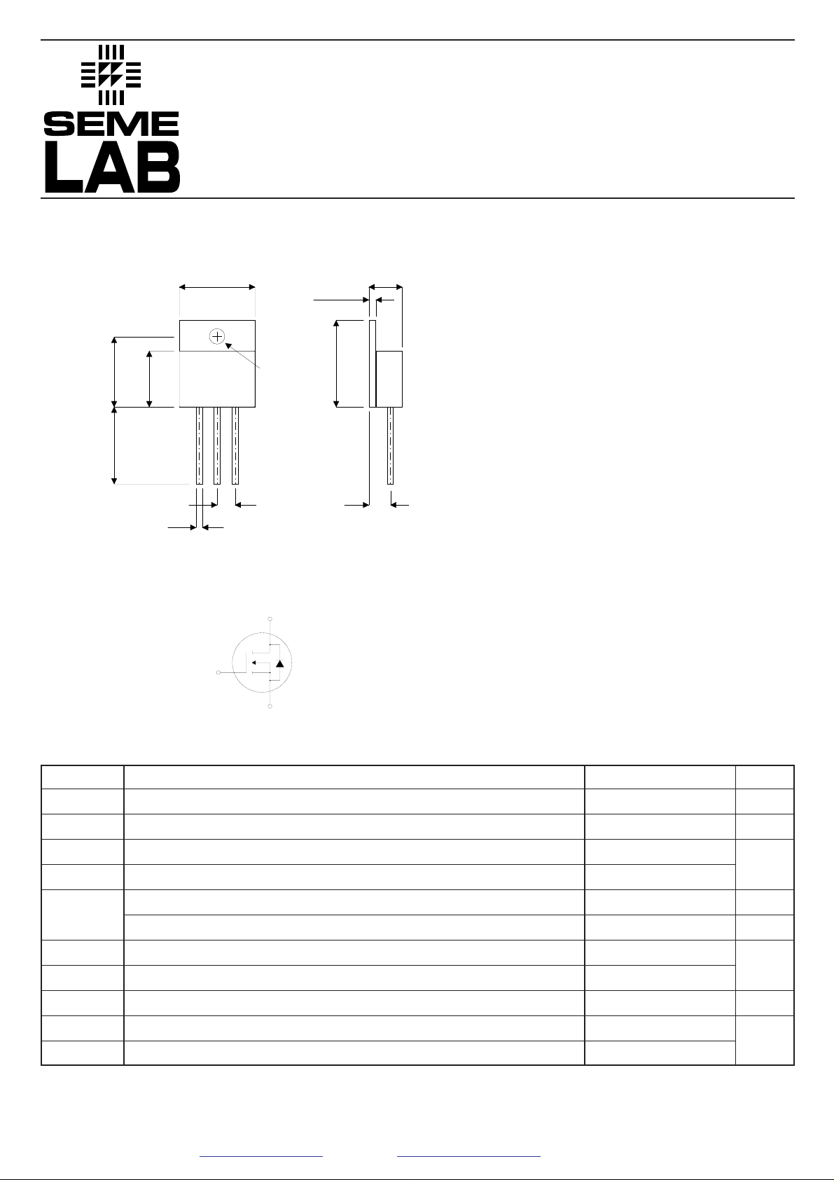
TO–258 Package Outline.
Dimensions in mm (inches)
SML60H16
6.86 (0.270)
21.21 (0.835)
20.70 (0.815)
6.09 (0.240)
3.56 (0.140)
BSC
17.65 (0.695)
17.39 (0.685)
4.19 (0.165)
3.94 (0.155)
17.96 (0.707)
17.70 (0.697)
13.84 (0.545)
13.58 (0.535)
19.05 (0.750)
12.70 (0.500)
Pin 1 – Drain Pin 2 – Source Pin 3 – Gate
123
5.08 (0.200)
1.65 (0.065)
1.39 (0.055)
Typ.
BSC
Dia.
1.14 (0.707)
0.88 (0.035)
D
G
S
N–CHANNEL
ENHANCEMENT MODE
HIGH VOLTAGE
POWER MOSFETS
V
DSS
I
D(cont)
R
DS(on)
• Faster Switching
• Lower Leakage
• TO–258 Hermetic Package
StarMOS is a new generation of high voltage
N–Channel enhancement mode power MOSFETs.
This new technology minimises the JFET effect,
increases packing density and reduces the
on-resistance. StarMOS also achieves faster
switching speeds through optimised gate layout.
600V
15.5A
0.370
ΩΩ
ABSOLUTE MAXIMUM RATINGS (T
V
DSS
I
D
I
DM
V
GS
V
GSM
P
D
TJ, T
T
L
I
AR
E
AR
E
AS
STG
Drain – Source Voltage
Continuous Drain Current
Pulsed Drain Current
1
Gate – Source Voltage
Gate – Source Voltage Transient
Total Power Dissipation @ T
Derate Linearly
Operating and Storage Junction Temperature Range
Lead Temperature : 0.063” from Case for 10 Sec.
1
Avalanche Current
(Repetitive and Non-Repetitive)
Repetitive Avalanche Energy
Single Pulse Avalanche Energy
1) Repetitive Rating: Pulse Width limited by maximum junction temperature.
2) Starting TJ= 25°C, L = 10.07mH, RG= 25Ω, Peak IL= 15.5A
= 25°C unless otherwise stated)
case
= 25°C
case
1
2
Semelab plc. Telephone +44(0)1455 556565. Fax +44(0)1455 552612.
E-mail: sales@semelab.co.uk
Website: http://www.semelab.co.uk
600
15.5
62
±30
±40
200
1.6
–55 to 150
300
15.5
30
1210
V
A
A
V
W
W/°C
°C
A
mJ
6/99
SML60H16
STATIC ELECTRICAL RATINGS (T
Characteristic Test Conditions Min. Typ. Max.Unit
BV
DSS
Drain – Source Breakdown Voltage
Zero Gate Voltage Drain Current
I
DSS
I
GSS
V
GS(TH)
I
D(ON)
R
DS(ON)
(VGS= 0V)
Gate – Source Leakage Current
Gate Threshold Voltage
On State Drain Current
2
Drain – Source On State Resistance
DYNAMIC CHARACTERISTICS
Characteristic Test Conditions Min. Typ. Max.Unit
C
iss
C
oss
C
rss
Q
g
Q
gs
Q
gd
t
d(on)
t
r
t
d(off)
t
f
Input Capacitance
Output Capacitance
Reverse Transfer Capacitance
Total Gate Charge
3
Gate – Source Charge
Gate – Drain (“Miller”) Charge
Turn–on Delay Time
Rise Time
Turn-off Delay Time
Fall Time
= 25°C unless otherwise stated)
case
VGS= 0V , ID= 250µA
VDS= V
VDS= 0.8V
VGS= ±30V , VDS= 0V
VDS= VGS, ID= 1.0mA
VDS> I
VGS= 10V
2
VGS= 10V , ID= 0.5 ID[Cont.]
VGS= 0V
VDS= 25V
f = 1MHz
VGS= 10V
VDD= 0.5 V
ID= ID[Cont.] @ 25°C
VGS= 15V
VDD= 0.5 V
ID= ID[Cont.] @ 25°C
RG= 1.6Ω
DSS
D(ON)
, TC= 125°C
DSS
x R
DS(ON)
DSS
DSS
Max
600
V
25
µA
250
±100
24
15.5
0.370
nA
V
A
Ω
3450 4140
403 565
pF
155 235
140 210
19 30
nC
68 100
12 24
12 24
ns
40 60
816
SOURCE – DRAIN DIODE RATINGS AND CHARACTERISTICS
Characteristic Test Conditions Min. Typ. Max.Unit
I
I
V
t
Q
S
SM
SD
rr
rr
Continuous Source Current
Pulsed Source Current
Diode Forward Voltage
1
2
Reverse Recovery Time
Reverse Recovery Charge
(Body Diode)
(Body Diode)
VGS= 0V , IS= – ID[Cont.]
IS= – ID[Cont.] , dls / dt = 100A/µs
IS= – ID[Cont.] , dls / dt = 100A/µs
THERMAL CHARACTERISTICS
Characteristic Min. Typ. Max.Unit
R
R
θJC
θJA
Junction to Case
Junction toAmbient
1) Repetitive Rating: Pulse Width limited by maximum junction temperature.
2) Pulse Test: Pulse Width < 380µS , Duty Cycle < 2%
3) See MIL–STD–750 Method 3471
CAUTION — Electrostatic Sensitive Devices. Anti-Static Procedures Must Be Followed.
Semelab plc.Telephone +44(0)1455 556565. Fax +44(0)1455 552612.
E-mail: sales@semelab.co.uk
Website: http://www.semelab.co.uk
450
8
15.5
62
1.3
0.62
40
A
V
ns
µC
°C/W
6/99
 Loading...