

Semelab Plc SML50T47 Datasheet
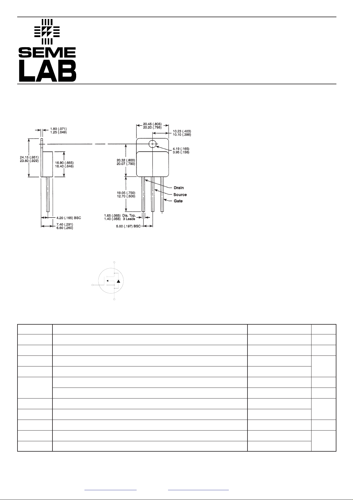
TO–267 Package Outline.
Dimensions in mm (inches)
SML50W40
N–CHANNEL
ENHANCEMENT MODE
HIGH VOLTAGE
POWER MOSFETS
D
G
S
ABSOLUTE MAXIMUM RATINGS (T
V
I
I
V
V
P
D
DM
DSS
GS
GSM
D
Drain – Source Voltage
Continuous Drain Current
Pulsed Drain Current
Gate – Source Voltage
Gate – Source Voltage Transient
Total Power Dissipation @ T
Derate Linearly
1
= 25°C unless otherwise stated)
case
= 25°C
case
V
DSS
I
D(cont)
R
DS(on)
500V
40A
0.120
ΩΩ
• Faster Switching
• Lower Leakage
• TO–267 Hermetic Package
StarMOS is a new generation of high voltage
N–Channel enhancement mode power MOSFETs.
This new technology minimises the JFET effect,
increases packing density and reduces the
on-resistance. StarMOS also achieves faster
switching speeds through optimised gate layout.
500
40
160
±30
±40
400
3.2
V
A
A
V
W
W/°C
TJ, T
T
L
I
AR
E
AR
E
AS
STG
Operating and Storage Junction Temperature Range
Lead Temperature : 0.063” from Case for 10 Sec.
1
Avalanche Current
Repetitive Avalanche Energy
Single Pulse Avalanche Energy
1) Repetitive Rating: Pulse Width limited by maximum junction temperature.
2) Starting TJ= 25°C, L = 3.13mH, RG= 25Ω, Peak IL= 40A
(Repetitive and Non-Repetitive)
1
2
Semelab plc. Telephone +44(0)1455 556565. Fax +44(0)1455 552612.
E-mail: sales@semelab.co.uk
Website: http://www.semelab.co.uk
–55 to 150
300
40
50
2500
°C
A
mJ
6/99

SML50W40
STATIC ELECTRICAL RATINGS (T
Characteristic Test Conditions Min. Typ. Max. Unit
BV
DSS
Drain – Source Breakdown Voltage
Zero Gate Voltage Drain Current
I
DSS
I
GSS
V
GS(TH)
I
D(ON)
R
DS(ON)
(VGS= 0V)
Gate – Source Leakage Current
Gate Threshold Voltage
On State Drain Current
2
Drain – Source On State Resistance
DYNAMIC CHARACTERISTICS
Characteristic Test Conditions Min. Typ. Max. Unit
C
iss
C
oss
C
rss
Q
g
Q
gs
Q
gd
t
d(on)
t
r
t
d(off)
t
f
Input Capacitance
Output Capacitance
Reverse Transfer Capacitance
Total Gate Charge
3
Gate – Source Charge
Gate – Drain (“Miller”) Charge
Turn–on Delay Time
Rise Time
Turn-off Delay Time
Fall Time
= 25°C unless otherwise stated)
case
VGS= 0V , ID= 250µA
VDS= V
VDS= 0.8V
VGS= ±30V , VDS= 0V
VDS= VGS, ID= 2.5mA
VDS> I
VGS= 10V
2
VGS= 10V , ID= 0.5 ID[Cont.]
VGS= 0V
VDS= 25V
f = 1MHz
VGS= 10V
VDD= 0.5 V
ID= ID[Cont.] @ 25°C
VGS= 15V
VDD= 0.5 V
ID= ID[Cont.] @ 25°C
RG= 0.6Ω
DSS
D(ON)
, TC= 125°C
DSS
x R
DS(ON)
DSS
DSS
Max
500
V
25
µA
250
±100
24
40
0.120
nA
V
A
Ω
7400 8900
1000 1400
pF
380 570
312 470
50 75
nC
127 190
14 30
16 32
ns
54 80
510
SOURCE – DRAIN DIODE RATINGS AND CHARACTERISTICS
Characteristic Test Conditions Min. Typ. Max. Unit
I
I
V
t
Q
S
SM
SD
rr
rr
Continuous Source Current
Pulsed Source Current
Diode Forward Voltage
1
2
Reverse Recovery Time
Reverse Recovery Charge
(Body Diode)
(Body Diode)
VGS= 0V , IS= – ID[Cont.]
IS= – ID[Cont.] , dls / dt = 100A/µs
IS= – ID[Cont.] , dls / dt = 100A/µs
THERMAL CHARACTERISTICS
Characteristic Min. Typ. Max. Unit
R
R
θJC
θJA
Junction to Case
Junction to Ambient
1) Repetitive Rating: Pulse Width limited by maximum junction temperature.
2) Pulse Test: Pulse Width < 380µS , Duty Cycle < 2%
3) See MIL–STD–750 Method 3471
CAUTION — Electrostatic Sensitive Devices. Anti-Static Procedures Must Be Followed.
Semelab plc. Telephone +44(0)1455 556565. Fax +44(0)1455 552612.
E-mail: sales@semelab.co.uk
Website: http://www.semelab.co.uk
620
14.7
40
160
1.3
0.31
40
A
V
ns
µC
°C/W
6/99
 Loading...